Strong electrically tunable exciton g-factors in individual quantum dots due to hole orbital angular momentum quenching.
Abstract
Strong electrically tunable exciton g-factors are observed in individual (Ga)InAs self-assembled quantum dots and the microscopic origin of the effect is explained. Realistic eight band simulations quantitatively account for our observations, simultaneously reproducing the exciton transition energy, DC Stark shift, diamagnetic shift and g-factor tunability for model dots with the measured size and a comparatively low In-composition of near the dot apex. We show that the observed g-factor tunability is dominated by the hole, the electron contributing only weakly. The electric field induced perturbation of the hole wavefunction is shown to impact upon the g-factor via orbital angular momentum quenching, the change of the In:Ga composition inside the envelope function playing only a minor role. Our results provide design rules for growing self-assembled quantum dots for electrical spin manipulation via electrical g-factor modulation.
pacs:
The spin of charge carriers in semiconductor quantum dots (QDs) has recently attracted much attention due to the promise it may provide for solid-state quantum information processing Hanson2007 ; Krenner2010 . In this respect, the need to selectively rotate a specific spin qubit within a quantum register, whilst simultaneously controlling interactions between spins is a challenging task. Such selective addressing either requires that each qubit has a unique resonance frequency or calls for highly local (nm) time dependent magnetic fields to selectively rotate a specific qubit Koppens2006 ; Kroner2008 . Methods to create nanoscale time dependent magnetic fields do not exist, motivating recent proposals for electrical spin control in both single layer Pingenot2008 QDs and QD-molecules Andlauer2009 via Land g-tensor modulation. Such approaches aim to tune the magnetic response using electric fields to push the carrier envelope functions into different regions of the nanostructure. This provides the potential to achieve arbitrary spin rotations on the Bloch sphere by applying time dependent electric fields Pingenot2008 ; Andlauer2009 using e.g. metallic gate structures. To date, electrical g-factor modulation in semiconductor nanostructures has been demonstrated using parabolically composition graded AlGaAs quantum wells Salis2001 and vertically coupled (Ga)InAs QD-molecules Doty2006 . However, very weak effects are typically observed for single dots Nakaoka2007 . Recently, we reported electrically tunable exciton g-factors in (Ga)InAs self-assembled QDs grown using the partially covered island (PCI) method but could not identify the mechanism responsible for the tuning Klotz2010 .
In this letter, we observe very strong electrical tunability of the exciton g-factor () in (Ga)InAs self-assembled QDs grown without the PCI method and unambiguously identify its microscopic origin. By performing realistic eight band simulations using a QD size, shape and In-composition determined by scanning tunneling microscopy, we quantitatively account for experimental results and obtain new insight into the origin of the effect. Our experimental and theoretical findings are in excellent agreement; exciton transition energy, DC Stark shift, diamagnetic shift and g-factor tunability all being simultaneously reproduced by theory using dots with a diameter , height and a maximum In-composition of near the dot apex. We show that the tunability is dominated by the hole (), the electron () contributing only weakly. Most surprisingly, the electric field induced perturbation of the hole envelope wavefunction is shown to impact upon principally via orbital angular momentum quenching pryor:2006 , the change of the In:Ga composition inside the envelope function playing only a minor role. The results show that the strength of the electrical tunability increases as the In-alloy content at the dot apex () reduces, explaining why we observe strong electrical tunability in our QDs.
The samples investigated were GaAs n-i-Schottky photodiode structures grown by molecular beam epitaxy. A single layer of nominally In0.5Ga0.5As self-assembled QDs was grown in the -region at an unusually high growth temperature of C. This is expected to lead to an average In-content significantly lower than the nominal value of , due to the combined effects of In-desorption Heyn2003a and inter-diffusion with the GaAs matrix material during capping Heyn2003b . Cross sectional STM measurements keizer:2010 indicate that the resulting dots have a lateral size of nm and height of nm.
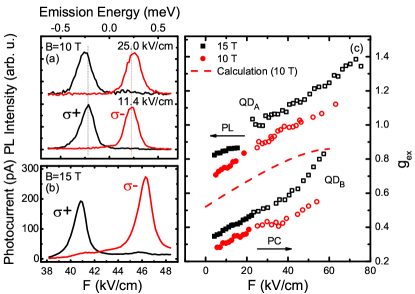
Single dots were optically probed using a low temperature ( K) magneto-confocal microscopy set up that facilitates application of magnetic () fields up to T in Faraday geometry. Typical PL spectra recorded at T and axial electric fields of kV/cm and kV/cm, respectively, are presented in fig.1a. The results clearly show two Zeeman split bright excitons with a degree of circular polarization. Upon raising the electric field we observe a clear increase of . For electric fields kV/cm the PL quenches due to carrier tunnelling from the dot and we probe the energy of the Zeeman branches using polarization selective photocurrent (PC) absorption measurements. PC spectra recorded with and polarized excitation were obtained at fixed laser frequency, whilst the levels were tuned into resonance via the DC-Stark effect. Typical results are plotted in fig.1b. The dependence of on the electric field is summarized in fig.1c for two representative QDs labelled and . For both , and all other dots investigated increases with the axial electric field.
To understand our results we performed electronic structure calculations using the eight band envelope function approximation. The magnetic field was introduced into the discrete Hamiltonian in a manifestly gauge invariant manner andlauer:2008 ; wilson:1974 and spatial finite volume discretization, combined with the correct operator ordering accounted for abrupt material boundaries burt:1999 . Strain fields were included using continuum elasticity theory and their impact on the electronic structure was taken into account via deformation potentials and the linear piezoelectric effect stier:1999 .
The direct Coulomb interaction was included in our calculations using lowest order perturbation theory and the validity of this approximation was carefully checked for a few selected cases where direct electron-hole Coulomb interaction was taken into account in a fully self consistent manner. To obtain quantitative results for the energy and g-factor, a Luttinger-like eight band -model was employed, where far-band contributions to the effective mass Hamiltonian and g-factors are included up to the order of trebin:1979 . We modeled our QDs as having a truncated lens shape with a diameter varying from nm, a height of nm above the wetting layer and an inverse trumpet-like In-compositional profile offermans:2005 ; migliorato:2002 . The In-concentration of the InGaAs alloy was taken to be at the base and side of the dot increasing to at the dot apex migliorato:2002 . This range of parameters are fully consistent with the results of cross sectional STM measurements performed on samples grown under the same conditions, from which we also determined the wetting layer thickness ( nm) and keizer:2010 .
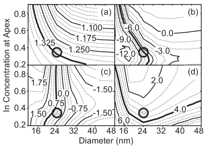
We continue to discuss the results of our calculations: Figures 2a, 2b and 2c show contour plots of the exciton transition energy at kV/cm, Stark shift from kV/cm and at T, respectively. Figure 2d shows the diamagnetic shift from T to T at an electric field of kV/cm. The measured values of these quantities for are represented by the bold contours on the figure, showing that all are reproduced in the , parameter space probed. More importantly, all of these contours intersect at nm and , as indicated by the open circles on the various panels of fig.2. We note that we also calculated very different g-factors for small ( nm), InAs rich () dots, in very good agreement with previous experiments and calculations nakaoka:2004 .
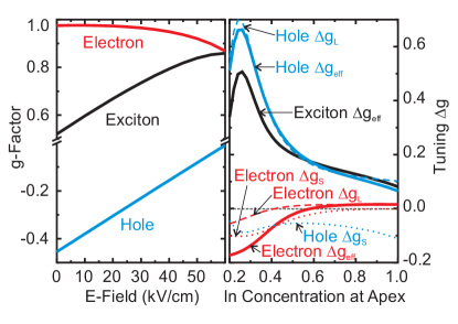
The electron and hole g-factors in self-assembled dots have been investigated in previous theoretical works; primary contributions arising from (i) strain induced band-mixing nakaoka:2005 , (ii) modification of Roth’s formula by the effective band-gap roth:1959 ; pryor:2006 and (iii) orbital angular momentum quenching kiselev:1998 ; lommer:1985 ; pryor:2006 . Electric field induced changes in the alloy overlap, i.e. the In-Ga content within the envelope function, have been shown to be important mostly for very extended electronic states in weakly confined dots pryor:2006 ; nakaoka:2004 . However, whilst each of the effects (i)-(iii) have been reported to contribute to , the microscopic origin of the strong electrical tunability in our samples is not at all obvious. We now demonstrate that the observed effects can be directly traced to strong electric field induced changes of the hole g-factor (), the electron g-factor () being much more weakly influenced by the electric field. The left panel of fig.3 shows representative calculations of , and for T using the model dot parameters deduced from fig.2 ( nm and ). Clearly varies only weakly over the range of electric fields investigated (), whilst is much more strongly affected ().
We now show that quenching of the orbital angular momentum in zero dimensional structures (mechanism - (iii)) is primarily responsible for the observed electrical tunability. The contributions to the g-factor of any electronic state with orbital index and spin orientation or ( and ) can be written as kiselev:1998
| (1) |
where is the free electron Land g-factor and is the contribution of remote bands included perturbatively in the 8-band model, a function of the In-content within the envelope function. In comparison, is the contribution to the g-factor due to the angular motion of the electron. This quantity can be obtained using second order perturbation theory and has the form,
| (2) |
with a momentum operator . The sum runs over all conduction and valence band states except . Here, is the 8-band momentum operator obtained by the Helman-Feynman theorem foreman:2000 and the quantization axis is taken to be , the direction of the applied static magnetic field. In a fully equivalent manner kiselev:1998 , we can also express in the framework of first order perturbation theory
| (3) |
with the orbital angular momentum operator . Eqn. 3 can be readily evaluated to obtain the tunability of the angular momentum g-factor . The right panel of fig.3 compares the calculated value of obtained from our full calculation (solid lines, labeled ) and the contributions from obtained using eqn. 3 (dashed lines) and the far band contribution (dotted lines) for .
We find several prominent features of which we highlight two: Firstly, the electric field tuning of is almost entirely due to the angular momentum contribution. In comparison, plays a much less important role for the electrical modification of . The electrically induced modification of the far-band correction () is weak for both hole and electron. Secondly, there is a clear maximum in the tunability of for low In-concentrations at the dot apex (). Thus, we conclude that the observed electrical tunability stems from the modification of the orbital angular momentum of the valence band state and that the low In-content of the presently studied QDs increases the strength of the effect. The increase of the angular momentum contribution to the hole ground state is equivalent to a decrease of angular momentum according to eqn. 3. Whilst we evaluated eqn. 3 to obtain the curves presented in the right panel of fig.3, we now make use of eqn. 2 to obtain a qualitative understanding of the observed tunability: The conduction band (CB) states in a III-V dot have large momentum matrix elements (MMEs), defined by in eqn. 3, with the valence band (VB) states. In particular, the MME between the lowest energy electron and hole orbital states without electric field is large. For In-dilute dots there are many bound hole states but only a few bound electron states. For example, we calculate that the best-fit QD from fig.2 with and accommodates bound hole states, but only 3 bound electron states. The electric field decreases the MME between specific pairs of bound CB and VB orbital states (e.g. lowest orbital states) whilst this modification is compensated by an increase of the MME between other orbital states according to the f-sum rule. For the electron ground state, there are many bound hole states available to compensate for the field induced reduction of the MME between the lowest CB and VB orbital. Each of these VB orbital states has approximately the same relative energy compared to the effective band gap of dot ( meV). Thus, the energy denominator of eqn. 2 is approximately the same for each pair of CB and VB states and there is almost no change in the angular momentum of the electron state and a weak tunability of . In strong contrast, for the lowest energy VB state there are very few bound CB states that can compensate for the field induced change of the MME. Thus, is strongly influenced by the electric field and dominates the observed tunability of .
It has been speculated that the change in alloy overlap may induce HH-LH mixing that could be responsible for the observed strong electrical tunability Klotz2010 , since the HH and LH g-factors differ strongly. However, our calculations show that ramping the electric field from kV/cm results in only a weak change of the LH admixture of the lowest VB orbital state (). Similarly, the electric field leads to no substantial change of the In:Ga alloy content within the hole envelope function. We calculated that for and nm, the In-alloy overlap changes by or for the hole and electron, respectively. This leads to an extremely weak change in the far-band correction as shown in the right panel of fig.3 and does not significantly contribute to the observed electric field tunability.
In summary, we identified the microscopic origin of pronounced electrical tunability of the exciton g-factor in composition engineered (Ga)InAs self-assembled QDs. We demonstrated that the tunability is dominated by , contributing only weakly. The electric field induced perturbation of the hole envelope wavefunction was shown to impact upon principally via orbital angular momentum quenching, the change of the In:Ga composition inside the envelope function playing only a minor role. Our results provide significant scope for morphological and structural tailoring self-assembled QDs to allow all electrical spin control via the g-tensor Pingenot2008 .
Acknowledgements.
This work is funded by the DFG via SFB-631 and NIM and the EU via SOLID. We gratefully acknowledge J. Keizer and P. Koenraad for useful discussions and for performing the X-STM measurements on our samples.References
- (1) R. Hanson, L. P. Kouwenhoven, J. R. Petta, S. Tarucha, and L. M. K. Vandersypen, Rev. Mod. Phys. 79, 1217 (2007)
- (2) H. J. K. O. Gywat and J. Berezovsky, Spins in Optically Active Quantum Dots (Wiley-VCH, 2010) ISBN 978-3-527-40806-1
- (3) F. H. L. Koppens, C. Buizert, K. J. Tielrooij, I. T. Vink, K. C. Nowack, T. Meunier, L. P. Kouwenhoven, and L. M. K. Vandersypen, Nature 442, 766 (2006)
- (4) M. Kroner, K. M. Weiss, B. Biedermann, S. Seidl, S. Manus, A. W. Holleitner, A. Badolato, P. M. Petroff, B. D. Gerardot, R. J. Warburton, and K. Karrai, Phys. Rev. Lett. 100, 156803 (2008)
- (5) J. Pingenot, C. E. Pryor, and M. E. Flatté, Appl. Phys. Lett. 92, 222502 (2008)
- (6) T. Andlauer and P. Vogl, Phys. Rev. B 79, 045307 (2009)
- (7) G. Salis, Y. Kato, K. Ensslin, D. C. Driscoll, A. C. Gossard, and D. D. Awschalom, Nature 414, 619 (2001)
- (8) M. F. Doty, M. Scheibner, I. Ponomarev, E. A. Stinaff, A. S. Bracker, V. L. Korenev, T. L. Reinecke, and D. Gammon, Phys. Rev. Lett. 97, 197202 (2006)
- (9) T. Nakaoka, S. Tarucha, and Y. Arakawa, Phys. Rev. B 76, 041301(R) (2007)
- (10) F. Klotz, V. Jovanov, J. Kierig, E. C. Clark, D. Rudolph, D. Heiss, M. Bichler, G. Abstreiter, M. S. Brandt, and J. J. Finley, Appl. Phys. Lett. 96, 053113 (2010)
- (11) C. Pryor and M. Flatte, Phys. Rev. Lett. 96, 026804 (2006)
- (12) C. Heyn and W. Hansen, Journal of Crystal Growth 251, 140 (2003)
- (13) C. Heyn and W. Hansen, Journal of Crystal Growth 251, 218 (2003)
- (14) J. G. Keizer, E. C. Clark, M. Bichler, G. Abstreiter, J. J. Finley, and P. M. Koenraad, Nanotechnology 21, 215705 (2010)
- (15) T. Andlauer, R. Morschl, and P. Vogl, Phys. Rev. B 78, 075317 (2008)
- (16) K. G. Wilson, Phys. Rev. D 10, 2445 (1974)
- (17) M. G. Burt, J. Phys.: Condens. Matter 11, R53 (1999)
- (18) O. Stier, M. Grundmann, and D. Bimberg, Phys. Rev. B 59, 5688 (1999)
- (19) H. Trebin, U. Rössler, and R. Ranvaud, Phys. Rev. B 20, 686 (1979)
- (20) P. Offermans, P. M. Koenraad, J. H. Wolter, K. Pierz, M. Roy, and P. A. Maksym, Phys. Rev. B 72, 165332 (2005)
- (21) M. A. Migliorato, A. G. Cullis, M. Fearn, and J. H. Jefferson, Phys. Rev. B 65, 115316 (2002)
- (22) J. Keizer, E. Clark, M. Bichler, G. Abstreiter, J. Finley, and P. Koenraad, IOP Nanotechnology 21, 215705 (2010)
- (23) T. Nakaoka, T. Saito, J. Tatebayashi, and Y. Arakawa, Phys. Rev. B 70, 235337 (2004)
- (24) T. Nakaoka, T. Saito, J. Tatebayashi, S. Hirose, T. Usuki, N. Yokoyama, and Y. Arakawa, Phys. Rev. B 71, 205301 (2005)
- (25) L. Roth, B. Lax, and S. Zwerdling, Phys. Rev. 114, 90 (1959)
- (26) A. Kiselev, E. Ivchenko, and U. Rössler, Phys. Rev. B 58, 16 353 (1998)
- (27) G. Lommer, F. Malcher, and U. Rössler, Phys. Rev. B RC 32, 6967 (1985)
- (28) B. A. Foreman, J. Phys.: Condens. Matter 12, R435 (2000)