Josephson Coupling and Fiske Dynamics in Ferromagnetic Tunnel Junctions
Abstract
We report on the fabrication of Nb/AlOx//Nb superconductor/insulator/ferromagnetic metal/superconductor (SIFS) Josephson junctions with high critical current densities, large normal resistance times area products, high quality factors, and very good spatial uniformity. For these junctions a transition from 0- to -coupling is observed for a thickness nm of the ferromagnetic interlayer. The magnetic field dependence of the -coupled junctions demonstrates good spatial homogeneity of the tunneling barrier and ferromagnetic interlayer. Magnetic characterization shows that the has an out-of-plane anisotropy and large saturation magnetization, indicating negligible dead layers at the interfaces. A careful analysis of Fiske modes provides information on the junction quality factor and the relevant damping mechanisms up to about 400 GHz. Whereas losses due to quasiparticle tunneling dominate at low frequencies, the damping is dominated by the finite surface resistance of the junction electrodes at high frequencies. High quality factors of up to 30 around 200 GHz have been achieved. Our analysis shows that the fabricated junctions are promising for applications in superconducting quantum circuits or quantum tunneling experiments.
pacs:
74.50.+rTunneling phenomena; Josephson effects and 74.45.+cProximity effects; Andreev reflection; SN and SNS junctions and 75.30.GwMagnetic anisotropy and 85.25.CpJosephson devices1 Introduction
The interplay between superconductivity (S) and ferromagnetism (F) at S/F-interfaces and more complex S/F-heterostructures results in a rich variety of interesting phenomena FuldePRA1964 ; Larkin1964 ; Bulaevskii1977 ; BuzdinRMP2004 ; Buzdin1982 ; Buzdin1992 . Examples are the oscillations in the critical temperature of S/F-bilayers with increasing F thickness Buzdin1982 ; JiangPRL1996 , oscillations in the critical current of SFS Josephson junctions RyazanovPRL2001 ; KontosPRL2002 ; SellierPRB2003 ; RyazanovJLTP2004 ; ObonzovPRL2006 , or the variation of the critical temperature of FSF trilayers as a function of the relative magnetization direction in the F layers GuPRL2002 . At an S/F-interface, the superconducting order parameter does not only decay in the F layer as at superconductor/normal metal (S/N) interfaces but shows a spatial oscillation resulting in a sign change. This oscillatory behavior is the direct consequence of the exchange splitting of the spin-up and spin-down subbands in the F layer, causing a finite momentum shift of the spin-up and spin-down electron of a Cooper pair leaking into the F layer BuzdinRMP2004 ; Buzdin1982 ; Buzdin1992 . Here, is the exchange energy and the Fermi velocity in the F layer. The decay and oscillatory behavior of the order parameter in the F layer can be described by the complex coherence length BuzdinRMP2004 ; Buzdin1982 ; Buzdin1992 ; DemlerPRB1997 ; BuzdinPRB2003 ; BergeretPRB2003 ; BergeretPRB2007 ; FaurePRB2006 . For the case of large exchange energy and negligible spin-flip scattering, with the diffusion coefficient in the F layer and the reduced Planck constant BuzdinRMP2004 ; Buzdin1992 ; BuzdinPRB2003 . The oscillatory behavior of the order parameter has been unambiguously proven by the observation of the -coupled state in SFS Josephson junctions RyazanovPRL2001 ; KontosPRL2002 ; SellierPRB2003 ; RyazanovJLTP2004 ; ObonzovPRL2006 ; Guichard2003 ; Blum2002 ; Bauer2004 ; Frolov2004 ; Robinson2006 ; WeidesAPL2008 ; PfeifferPRB2008 ; Petkovic2009 ; Khaire2009 . Here, the ground state has a phase difference of between the macroscopic superconducting wave functions in the junction electrodes. Therefore, -junctions have an anomalous current-phase relation corresponding to a negative critical current Bulaevskii1977 ; DemlerPRB1997 . Using Josephson junctions with a step-like F layer thickness, also junctions with a coupling changing between and along the junction have been realized BuzdinPRB2003b ; WeidesPRL2006 ; WeidesJAP2007 .
An interesting application of -coupled Josephson junctions are -phase shifters in superconducting quantum circuits. For example, superconducting flux quantum bits Orlando1999 ; Chiorescu2003 ; DeppePRB2007 ; Deppe2008a ; Niemczyk2009a ; Niemczyk2010a require an external flux bias to operate them at the degeneracy point. Here, is the flux quantum with the elementary charge and is an integer. This requirement makes flux qubits susceptible to flux noise, which may be introduced through the flux biasing circuitry. Furthermore, to operate a cluster of (coupled) flux qubits, which inevitably will have a spread in parameters, requires an individual and precise flux bias for each qubit. To circumvent this problem the insertion of -phase shifters into the flux qubit loop has been suggested BlatterPRB2001 ; Yamashita2005 ; Yamashita2006 ; Ioffe1999 and successfully demonstrated recently Feofanov2010 . The applications of -coupled Josephson junctions in classical or quantum circuits in most cases requires high critical current densities and high critical current times normal resistance products, . Furthermore, they are not allowed to deteriorate the coherence properties when used in superconducting quantum circuits. Potential sources of decoherence are for instance spin-flip processes in the F layer or the dynamic response of the magnetic domain structure. Another serious difficulty comes from dissipation due to quasiparticle excitation. It has been shown recently, that long decoherence times require junctions with both high and large normal resistance times area products, KatoPRB2007 . This is difficult to be achieved in SFS junctions due to the low resistivity of the metallic F layer. However, the situation can be improved by inserting an additional insulating barrier, resulting in a superconductor/insulator/ferromagnet/superconductor (SIFS) stack. Here, much higher values at modest can be achieved. In particular, underdamped SIFS Josephson junctions can be realized allowing for the study of the junctions dynamics. Therefore, there has been strong interest in SIFS junctions recently PfeifferPRB2008 ; Petkovic2009 .
In this article we report on the fabrication as well as the static and dynamic properties of a series of Nb/AlOx//Nb (SIFS) Josephson junctions with different thickness of the ferromagnetic interlayer. We succeeded in the fabrication of junctions with high and values resulting in high junction quality factors . We discuss the dependence of the product on the thickness of the F layer, including the transition from - to -coupling. We also address the magnetic properties of the F interlayer in the magnetic field dependence of the critical current. Special focus is put on the analysis of Fiske modes. Comparing these resonant modes to theoretical models allows us to evaluate the quality factors of the junctions over a wide frequency range from about 10 to 400 GHz and to determine the dominating damping mechanisms.
2 Sample Preparation and Experimental Techniques
The fabrication of SIFS Josephson junctions with controllable and reproducible properties was realized by the deposition of Nb/AlOx//Nb multilayers by UHV dc magnetron sputtering and subsequent patterning of this multilayer stack using optical lithography, a lift-off process, as well as reactive ion etching (RIE). Thermally oxidized silicon wafers ( nm oxide thickness) were used as substrates.
In a first step the whole Nb/AlOx//Nb (SIFS) multilayer stack was sputter deposited in-situ in a UHV dc magnetron sputtering system with a background pressure in the low mbar range. This system is equipped with three sputter guns (Nb, , Al) and an Ar ion beam gun for surface cleaning. The sputtering chamber is attached to a UHV cluster tool, allowing for the transfer of the samples to an AFM/STM system for surface characterization without breaking vacuum. The multilayer stack consists of a niobium base electrode with thickness nm, an aluminum layer of thickness nm, a ferromagnetic (PdNi) interlayer with thickness ranging between 4 and 15 nm, and finally a niobium top electrode with thickness nm. The reproducible fabrication of ferromagnetic SIFS Josephson junctions requires the precise control of the thickness of the PdNi layer and the minimization of the roughness of the involved interfaces. Therefore, we have carefully optimized the parameters of the sputtering process (Ar pressure, power, substrate-target distance) for both the Nb and PdNi layers to obtain films with very smooth surfaces. After optimization, the rms roughness of the Nb base electrode was reduced to nm. The ferromagnetic PdNi layers showed a slightly larger rms roughness of nm. For the deposition of Nb and Al an Ar pressure of mbar was used, resulting in a deposition rate of 0.7 nm/s at 200 W for niobium and 0.2 nm/s at 40 W for aluminum, respectively. PdNi was sputtered at a higher Ar pressure of mbar, resulting in a growth rate of 0.4 nm/s at 40 W. The transition temperature of the Nb films was K and the Curie temperature of the PdNi films was determined to about 150 K by SQUID magnetometry.
A critical process step in the deposition of the Nb/AlOx//Nb (SIFS) multilayer stack is the fabrication of the tunneling barrier. To achieve good reproducibility, the tunneling barrier was realized by partial thermal oxidation of the 4 nm thick Al layer inside the sputtering chamber. The thickness of the AlOx tunneling barrier was adjusted by varying the oxygen partial pressure and the duration of the thermal oxidation process. The oxidation time was varied between 60 and 240 min in a pure oxygen atmosphere of 0.1 mbar. We note that the thickness of the AlOx tunneling barrier determines the values of the junctions, because the tunneling resistance is much larger than the resistance of the layer.
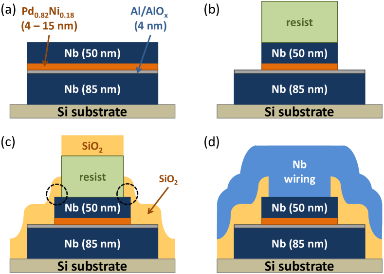
After the controlled in-situ deposition of the Nb/AlOx//Nb multilayer stack, in the next step the SIFS Josephson junctions are fabricated by a suitable patterning process. We used a three-stage self-aligned process based on optical lithography, a lift-off process and reactive ion etching (RIE). In the first step, the base electrode is defined by patterning a long about m wide strip into the whole multilayer stack. This is achieved by placing a suitable photoresist stencil on the Si substrate and using a lift-off process after the deposition of the SIFS multilayer stack. Fig. 1a shows a cross-sectional view of the SIFS multilayer after this step. Next, the junction area is patterned by etching a mesa structure into the SIFS stack by placing a photoresist stencil on top of the SIFS stack. This resist stencil serves as the etching mask in a RIE patterning process thereby defining the shape and size of the junction area. Junction areas between m2 and m2 have been realized. The RIE process was performed in a SF6 plasma (time: 70 s, voltage: 300 V). Note that the RIE process selectively patterns the Nb top electrode and the PdNi layer because the AlOx layer acts as an effective stopping layer. The resist stencil defining the junction area is used for the lift-off process in the subsequent deposition of the SiO2 wiring insulation (self-aligned process). To avoid electrical shorts between the wiring layer for the top electrode and the base electrode, the lateral dimensions of the resist mask were reduced by about nm using an oxygen plasma process in the RIE system immediately after the mesa patterning. In this way, the SiO2 wiring insulation also covers the junction edges, preventing electrical shorts (cf. Fig. 1c). The 50 nm thick SiO2 wiring insulation is deposited by rf-magnetron sputtering in a 75%Ar/25%O2 atmosphere. In a last step, the 200 nm thick niobium wiring layer is deposited. The Nb deposition was done by dc magnetron sputtering and the patterning was realized by optical lithography and a subsequent lift-off process. To obtain a good superconducting contact between the Nb wiring layer and the Nb top electrode, the surface of the top electrode has been cleaned in-situ prior to the deposition of the wiring layer using an Ar ion gun. A cross-sectional view of the completed junction is shown in Fig. 1d. Of course, the junction fabrication process allows for the fabrication of several junctions with different junction areas on the same wafer. In this way the reproducibility of the process can be checked by measuring the on-chip parameter spread.
The characterization of the junctions was performed in a 3He cryostat and a 3He/4He dilution refrigerator, allowing temperatures down to 300 mK and 20 mK, respectively. The dilution refrigerator was placed in a rf-shielded room to reduce high-frequency noise. Furthermore, external magnetic fields have been reduced by -metal and/or cryoperm shields. Small magnetic fields aligned parallel to the junction barrier could be applied by a superconducting Helmholtz coil. The current-voltage characteristics (IVCs) have been measured in a four-point configuration. A low-noise current source and voltage preamplifier (Stanford Research SR 560) have been used. Both were battery powered and placed inside the rf-shielded room. Derivatives of the IVCs have been taken using a lock-in technique. The magnetic properties of the ferromagnetic interlayer have been measured using a Quantum Design SQUID magnetometer.
3 Superconducting and Magnetic Properties
In this section we discuss the superconducting and magnetic properties of the SIFS Josephson junctions fabricated with the process described above. In particular, we will address the magnetic properties of the layer and the dependence of the product of critical current and normal resistance of the junctions on the thickness of the ferromagnetic interlayer. We will see that this dependence shows a clear transition from - to -coupled junctions at nm. In this article we will focus mainly on the properties of the -coupled SIFS junctions. We will discuss their current-voltage characteristics (IVCs) and their magnetic field dependence of the critical current, allowing us to determine the basic parameters of the SIFS junctions.
3.1 Magnetic Properties of the PdNi Layer
The Curie temperature of the layer has been determined to about 150 K by measuring the magnetization versus temperature dependence using a Quantum Design SQUID magnetometer. For thin ferromagnetic films the easy axis of the magnetization usually is parallel to the film plane to minimize the free energy contribution due to the shape anisotropy. However, in very thin films the magnetic surface energy may be dominant resulting in an easy axis perpendicular to the film plane. To get information on the direction of the easy axis we have recorded the magnetization versus applied magnetic field curves of the thin layer within a Nb/AlOx//Nb multilayer stack with the magnetic field applied in- and out-of-plane. The result is shown in Fig. 2. Qualitatively, an almost rectangularly shaped curve is expected for the field applied along the easy axis because the magnetization tries to stay along this preferred direction as long as possible and than abruptly switches to the opposite direction at the coercive field. In contrast, for the field applied along the hard axis the magnetization is expected to be gradually rotated out of the easy axis direction into the hard axis direction on increasing the applied magnetic field, resulting in a gradually increasing and decreasing magnetization when sweeping the field. As demonstrated by Fig. 2, the measured curve is much more rounded and has smaller remanent magnetization, when the field is applied in-plane, whereas it has an almost rectangular shape when the field is applied out-of-plane. This is clear evidence for an out-of-plane anisotropy of the PdNi film. That is, the out-of-plane (in-plane) direction is the magnetic easy (hard) axis in agreement with literature Khaire2009 . An out-of-plane anisotropy has been observed also for CuNi Ruotolo2004 . A more detailed analysis of the magnetic anisotropy of the PdNi films would require additional experiments such as ferromagnetic resonance and methods providing information on the domain structure. However, it is difficult to perform such experiments with ferromagnetic layers enclosed by two metallic Nb layers.
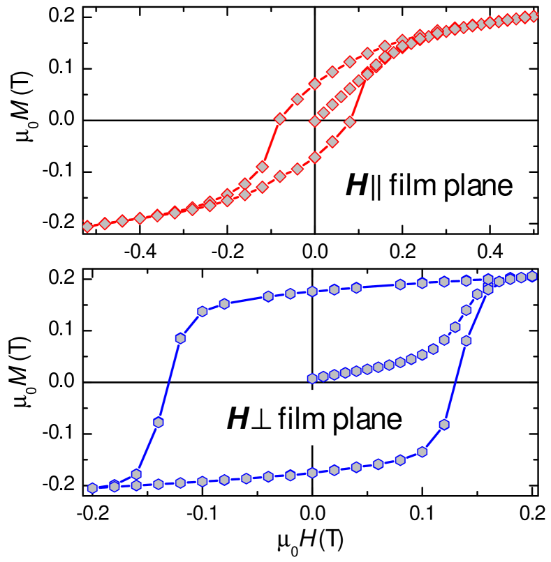
The saturation magnetization of the layer is about T in good agreement with literature values Khaire2009 . This magnetization corresponds to a magnetic moment of slightly above per Ni atom, if one assumes that there is negligible contribution of Pd. Here, is Bohr’s magneton. This is close to the values in polycrystalline bulk samples, for which and has been reported CablePRB1970 . This suggests that there are no significant magnetic dead layers. Since was measured with an only 8 nm thick PdNi film, even very thin dead layers at the interfaces would result in a significant reduction of . In the measurement of the magnetic field dependence of the critical current of the SIFS junctions only an in-plane magnetic field of the order of a few mT is applied. In this small field range only the virgin curve is relevant, which is about linear and almost non-hysteretic. From the experimental data taken at 11 K the slope of the curve is determined to .
3.2 Crossover between 0- and -Coupling
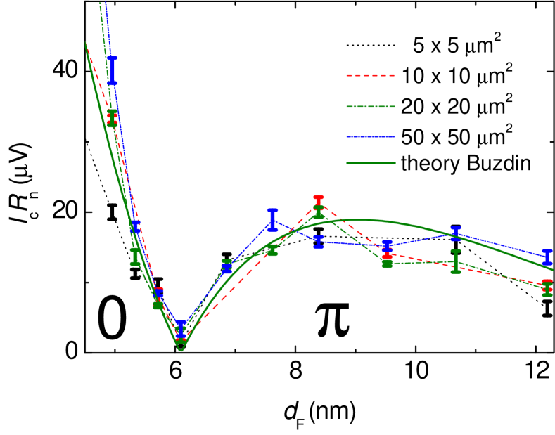
We next discuss the dependence of the characteristic junction voltage on the thickness of the ferromagnetic interlayer. The values of a large number of junctions with different and junction areas ranging from to are plotted in Fig. 3 versus the thickness of the F layer. To achieve this data, a series of junctions with different was fabricated with otherwise identical parameters. In particular, all junctions have AlOx barriers obtained by a 90 min long thermal oxidation process, resulting in m2. This series clearly shows a change of sign in the slope of the dependence at a layer thickness of nm. At this value approaches zero. This feature is a clear signature of the crossover from - to -coupling on increasing , corresponding to a change of sign of . Obviously, in the experiment we can only measure the modulus of .
In order to theoretically describe the behavior shown in Fig. 3 one has to distinguish different regimes defined by three energy scales BuzdinRMP2004 . These scales are the exchange energy in the ferromagnet, the energy gap of the superconductor, and , where is the elastic scattering time in the ferromagnet. In our samples, ( meV for Nb) as in the overwhelming part of other reports on SFS or SIFS junctions. However, there is a significant variation in relative to the other two energy scales. The true clean-limit holds for . In this case the mean free path is large compared to the clean-limit superconducting coherence length and exchange length . Here, is the Fermi velocity in the respective material. The true dirty limit holds for . In this case the mean free path is the smallest length scale and the dirty-limit superconducting coherence length and exchange length are given by the geometric mean. Here, is the diffusion coefficient in the respective material. There is also an intermediate regime, where and , which is the most complicated situation. This regime may particularly apply for a ferromagnet with large .
Due to the small mean free path in the PdNi alloy and Nb films, for our samples the simple dirty limit holds. Several theoretical models have been proposed for this limit BuzdinRMP2004 ; KontosPRL2002 ; DemlerPRB1997 ; BuzdinPRB2003 ; BergeretPRB2003 ; BergeretPRB2007 ; FaurePRB2006 . For weak ferromagnets such as PdNi the spin-up and spin-down subbands can be treated identically (same Fermi velocity and mean free path) resulting in a single characteristic length scale
| (1) |
for the decay and oscillation of the critical current as a function of . We note, however, that in the presence of spin-flip or spin-orbit scattering the decay and oscillation of is governed by two different length scales DemlerPRB1997 ; BergeretPRB2003 ; BergeretPRB2007 ; FaurePRB2006 .
The solid olive line in Fig. 3 is obtained by fitting the data using the simple dirty limit expression of Buzdin et al. BuzdinPRB2003 . The fit yields nm and V. Here, K is the critical temperature of the niobium layers and and are the superconducting order parameters just at the boundary with the ferromagnetic layer. They are certainly much smaller than the superconducting gap in bulk niobium but difficult to be determined in the geometry of our experiment. The value nm found for our SIFS junctions agrees very well with literature values KontosPRL2002 ; BuzdinPRB2003 ; KontosPRL2001 . The value of V found for for our SIFS junctions is larger than the value of V obtained by Kontos and coworkers KontosPRL2002 ; BuzdinPRB2003 . Unfortunately, the detailed comparison of different experiments is difficult because the authors often do not state whether they are plotting or . If we use the much higher subgap resistance , the corresponding value derived for would be about ten times larger. We finally note that the measured dependence can be well explained by dirty limit theory with a single length scale , suggesting that spin-flip or spin-orbit scattering do not play a dominant role.
Beyond the parameter describing the characteristic length of superconducting correlations in the F layer, the dimensionless parameter
| (2) |
is used to describe ferromagnetic Josephson junctions. It characterizes the transparency of the F/S interfaces with the interface resistance times area and the conductivity of the F layer. In general, two values for the two F/S interfaces have to be used. In our experiment the presence of the additional AlOx barrier at one S/F boundary can be modeled by a very low transparency interface (), while the other boundary has high transparency () for the in-situ fabricated stacks, i.e. . We further note that in general the measured total product can be expressed as
| (3) |
Here, and are the resistance times area values due to the tunneling barrier and the PdNi/Nb interfaces. For our junctions, and, moreover, . With we estimate which is by about five orders of magnitude smaller than the measured values. That is, the contribution of the F layer to is negligible. Hence, , meaning that the measured values are dominated by the AlOx tunneling barrier as expected. In this case we can write . With , nm and the measured value of about for this junction series we estimate . This high value is not surprising due to the additional tunneling barrier in our junctions.
The derived values can be used to estimate the exchange energy in PdNi. Using a Fermi velocity m/s DyePRB1981 and the fact that the mean free path for the very thin PdNi layers is about given by the film thickness , we obtain m2/s for nm. With this value we derive meV using nm. This value is in good agreement with values between about 10 and 50 meV quoted in previous work KontosPRL2002 ; Bauer2004 ; Khaire2009 ; CirilloPRB2005 . With the same numbers we obtain meV. This shows that the SIFS junctions with PdNi interlayer are close to the intermediate regime since .
3.3 IVCs and Magnetic Field Dependence of the Critical Current
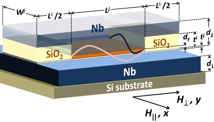
In the following we discuss the IVCs and magnetic field dependence of the critical current. We focus on SIFS junctions with a F layer thickness of nm resulting in -coupling. The AlOx tunneling barrier has been achieved by thermal oxidation for 4 h in pure oxygen to obtain high values and, in turn, low damping of the self excited resonances. We start our discussion by considering the effect of the specific junction geometry (cf. Fig. 4) used in our experiments on the derived junction parameters. Although these effects are often neglected in literature, it is mandatory to take them into account in a detailed evaluation. Of particular importance are the finite thickness of the junction electrodes and the so-called idle region. The latter is formed when the wiring of the top electrode is deposited to complete the junction structure. Then the bottom electrode, the SiO2 wiring insulation and the wiring layer are forming an SIS structure next to the junction area.
Effective Magnetic Thickness
It is well known that a magnetic field applied parallel to the surface of a bulk superconductor decays exponentially inside the superconductor due to the Meißner effect Tinkham . The characteristic screening length is the London penetration depth which is about 90 nm for Nb Kohlstedt1995 . However, in our junctions we are using electrodes of finite thickness . In such a thin film superconductor the magnetic field dependence perpendicular to the film (-direction) is obtained to
| (4) | |||||
by solving the London equations Tinkham . Here, the film is assumed to extend from to , and and are the external magnetic fields applied parallel to the film at both sides. The boundary conditions and the resulting current distributions are different for different physical situations. If the field is confined on one side of the superconducting film, we have and . For Josephson junctions this situation applies to cases where one is considering only the fields related to supercurrents flowing in the junction electrodes. If , screening currents are confined to a length scale smaller than , resulting in an enhanced kinetic inductance as compared to a bulk superconductor with Swihart61 . That is, the thin film superconductor behaves equivalent to the bulk one with an effective screening length . Then, the magnetic penetration in the barrier layer and the junction electrodes can be described by the effective magnetic thickness
| (5) |
Here, is the thickness of the oxide barrier, the thickness of the F layer, and are the thicknesses of the Nb junction electrodes, and and the corresponding penetration depths. For our junctions we have nm (we assume for simplicity that the oxide thickness is equal to the thickness of the Al layer), nm, nm, nm Kohlstedt1995 , nm and resulting in nm. For the idle region next to the junction area (cf. Fig. 4) an expression equivalent to eq.(5) is obtained by replacing by on the right hand side and setting .
Another interesting case is the situation where the same magnetic field is applied at both sides of the superconducting film. Here, and hence . This case applies when we are measuring the dependence of the junction critical current on a magnetic field applied parallel to the junction electrodes. Since the junction (we are considering only short junctions here) cannot screen the applied field from the region between the junction electrodes, the same field is present at both surfaces of the junction electrodes. To derive an effective magnetic thickness for this situation we consider the total flux threading the junction. The latter is obtained by integrating eq.(4) along the -direction. Whereas for bulk electrodes (, for thin film electrodes we obtain . That is, regarding the flux the thin film superconductor behaves equivalent to the bulk one with an effective screening length . Then, for the description of the total flux threading the junction we can use the effective magnetic thickness Weihnacht1969
| (6) |
Effective Swihart Velocity and Frequencies of Resonant Modes
The idle region shown in Fig. 4 influences the dynamic properties of the junction. The reason is that the idle region acts as a dispersive transmission line parallel to the junction edges. As discussed in detail in section 4, the junction forms a transmission line resonator supporting so-called Fiske resonances PhysRevFiske . For a junction without any idle region these resonances appear at frequencies corresponding to voltages
| (7) |
Here and
| (8) |
is the Swihart velocity Swihart61 with the velocity of light in vacuum. Evidently, as the junction barrier thickness is by almost two orders of magnitude smaller than the effective magnetic thickness of the junction.
For a junction with idle region, the resonance frequencies and corresponding voltages are shifted. We first discuss the effect of a lateral idle region extending parallel to the resonant mode. In this case we have to consider the junction transmission line in parallel with the two transmission lines of the idle regions at both sides of the junction. To each isolated transmission line we can assign the inductance and capacitance each per unit length, where the indices and refer to the idle and junction region. The corresponding phase velocities are with . The phase velocity of the combined transmission lines is given by with and . Evidently, the idle region increases the capacitance and decreases the inductance per unit length. However, the inductance effect is dominant since usually . This is true also for our samples. Therefore, the phase velocity is increased by the idle region. A more detailed analysis yields Lee91 ; IEEEApplSup2Lee ; Monaco1995
| (9) |
We next discuss the effect of a longitudinal idle region extending perpendicular to the resonant mode. In this situation the idle region can be considered as a lumped capacitance loading the junction at its ends, since the wave length usually is much larger than the dimension of the idle region. For short junctions () detailed calculations yield Monaco1995
| (10) |
Here, is the lumped load capacitance and the total junction capacitance. We see that the effect of is to decrease the phase velocity. However, since usually we have , that is, the effect is quite small even if the idle region has similar area as the junction. With nm, , nm, , nm, nm and (typical for a junction) we estimate for the lateral and for the longitudinal mode.
Current-Voltage Characteristics
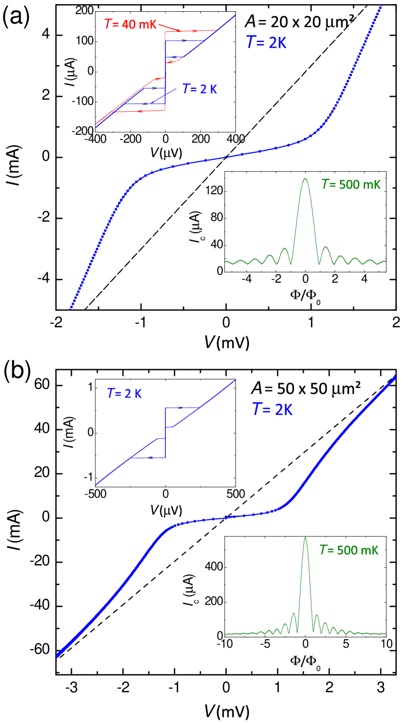
Figure 5 shows the IVCs of two -coupled SIFS junctions with junction areas m2 and m2. From the IVCs we can determine several relevant junction parameters. First, the current value for the switching from the zero to the finite voltage state and vice versa gives the critical current and the so-called retrapping current (see insets of Fig. 5). The corresponding current densities and are obtained by dividing by the junction area . From together with the effective magnetic thickness of the junction (cf. eq.(5)) the Josephson penetration depth is derived. At K we obtain . Since this value is larger than the lateral junction dimensions, we are dealing with small Josephson junctions. Using the simple resistively and capacitively shunted junction (RCSJ) model APLstewart , we can further derive the junction quality factor . Here, is the Stewart-McCumber parameter, the junction plasma frequency, and the time constant of the junction. Second, from the asymptotic behavior at voltages large compared to the gap sum voltage the normal resistance and the normal resistance times area product, , are obtained which are about temperature independent. The value has to be distinguished from the temperature dependent subgap resistance obtained from the slope of the IVCs at voltages well below the gap sum voltage. For SIFS junctions, is expected to increase with decreasing temperature in agreement with the experimental data. At 2 K, for our SIFS junctions is almost an order of magnitude larger than .
We note that the values of and may be reduced and enhanced, respectively, by premature switching due to thermal activation or external high-frequency noise. This is particularly true for small area junctions with small absolute values of and . In turn, this results in reduced values of the quality factor. This effect is shown in the inset of Fig. 5a, where the IVCs of a m2 junction are shown for K and 40 mK. The 40 mK data were taken in a well shielded dilution refrigerator using various filters at different temperature stages in the current and voltage lines, including stainless steel powder filters. Clearly, at 40 mK significantly larger and smaller values are observed resulting in an about three times larger quality factor . These enhanced/reduced values are only partly caused by lowering the temperature but mostly by the reduced thermal and external noise. For large area junctions this effect is negligible. Here, and are large, making the relative effect of the equivalent noise current very small. For example, at K is obtained for the m2 junction, whereas for the m2 junction fabricated on the same chip. This small quality factor is related to the smaller and values of the small area junction, making it more susceptible to thermal and external noise. In Table 1 we have tabulated the junction parameters derived from the IVCs of the m2 and m2 junction at 2 K and 40 mK, respectively.
| (m2) | ||
|---|---|---|
| (K) | 40 mK | 2K |
| (A) | 131 | 555 |
| (A/cm2) | 33 | 22 |
| (A) | 27 | 125 |
| () | 0.33 | 0.051 |
| (m2) | 133 | 128 |
| () | 2.14 | 0.44 |
| (V) | 44 | 28.3 |
| (V) | 280 | 244 |
| m) | 59 | 71 |
| 6.2 | 5.7 |
Magnetic Field Dependence of the Critical Current
The bottom insets in Fig. 5 show the magnetic field dependence of the critical current of the SIFS Josephson junctions measured at mK. The dependencies are close to a Fraunhofer diffraction pattern
| (11) |
expected for an ideal short Josephson junction with a spatially uniform . This demonstrates that our SIFS junctions have good uniformity of across the junction area, that is, a spatially homogeneous tunneling barrier and ferromagnetic interlayer. In particular, there are no short circuits at the junction edges or the surrounding SiO2 wiring insulation. We note that direct information on junction inhomogeneities on smaller length scales can be obtained by Low Temperature Scanning Electron Microscopy GrossRPP1994 ; BoschPRL1985 ; FischerScience1994 ; GerdemannJAP1994 .
We note that the total flux threading the junction is composed of the flux due to the applied external magnetic field and the flux due to the magnetization of the ferromagnetic layer. The two components are given by
| (12) | |||||
| (13) |
Here, is the lateral dimension of the rectangular junction perpendicular to the field direction, the thickness of the F interlayer, and the effective magnetic thickness of the junction given by eq.(6). Since the applied magnetic field required for the generation of a single flux quantum in the junction is less than about 1 mT for , the typical field range used in the measurement of the curves of Fig. 5 is restricted to less than about 10 mT. For such small in-plane magnetic fields the curve of the ferromagnetic PdNi layer (cf. Fig. 2) can be well approximated by a linear dependence with . With this approximation the total magnetic flux threading the junction can be expressed as
| (14) | |||||
Here, is the magnetization component parallel to the applied magnetic field. If there is a significant in-plane magnetic anisotropy of the ferromagnetic material, this component may be much smaller than the absolute value of the magnetization. Furthermore, there may be a complicated domain structure. In this case, is the average magnetization parallel to the field direction.
We can use (14) to estimate the magnitude of the additional flux due to the F layer. For the junctions of Fig. 5, nm and hence . Therefore, for the second summand in the brackets of (14) amounts to only about 0.04. That is, compared to a junction without F interlayer the total flux is enhanced only by about 4%. Due to the uncertainties in and the geometrical dimensions of the junctions, this small effect is difficult to prove. Furthermore, since the virgin part of the hard axis curve of the PdNi layer is about linear at small fields with negligible hysteresis, the curves are expected to show negligible hysteresis on sweeping back and forth the applied magnetic field. This is in agreement with our data and measurements on SIFS junctions with ferromagnetic CuNi interlayers Weides2008 . We note, however, that strongly depends on magnetic history. After having increased the applied field to large values saturating the F layer, there is a significant remanent magnetization on reducing the field to zero again. This remanence causes a large which may exceed . Unfortunately, applying high magnetic fields also results in the trapping of Abrikosov vortices in the Nb junction electrodes, making the interpretation of the measured dependencies difficult.
4 Fiske Resonances
According to the Josephson equations, the supercurrent across a Josephson junction oscillates at a constant frequency when a constant voltage is applied across the junction Josephson . On the other hand, the junction geometry forms a transmission line resonator of length (cf. Fig. 4) with resonance frequencies . Here, and is the Swihart velocity Swihart61 . At an applied junction voltage , the oscillation frequency of the Josephson current matches the -th harmonic of the junction cavity mode, potentially resulting in the excitation of the cavity modes. The excitation of the cavity resonances is most effective, if the spatial period of the Josephson current distribution along the junction is about matching the spatial period of the -th resonant electromagnetic mode of the junction. Since for short junctions the Josephson current density is spatially uniform at zero magnetic field, there is no excitation of the resonant modes. However, a spatial modulation can be easily achieved by applying a magnetic field. The resonance is a highly nonlinear process which results in self-induced current steps at in the IVCs denoted as Fiske steps PhysRevFiske ; RMPFiske ; Barone . These steps are clearly visible in the IVCs shown in Fig. 6 and their derivatives plotted in Fig. 7. The data were obtained for a junction with area recorded at different magnetic fields applied parallel (-direction) and perpendicular (-direction) to the bottom electrode. The vs. curves were measured by a lock-in technique. In the case of negligible damping the resonances are very sharp at almost constant voltages. However, in reality the resonances are damped due to different loss mechanisms. For planar type SIFS junctions as studied in our work the junction damping due to radiation losses is small due to the large electromagnetic impedance mismatch at the junction boundaries. Then, the quality factors of the Fiske resonances are given mainly by the internal losses, most likely due to quasiparticle tunneling and the finite surface resistance. In general, the detailed analysis of the Fiske resonances can provide information on the damping mechanisms in Josephson junctions at very high frequencies.
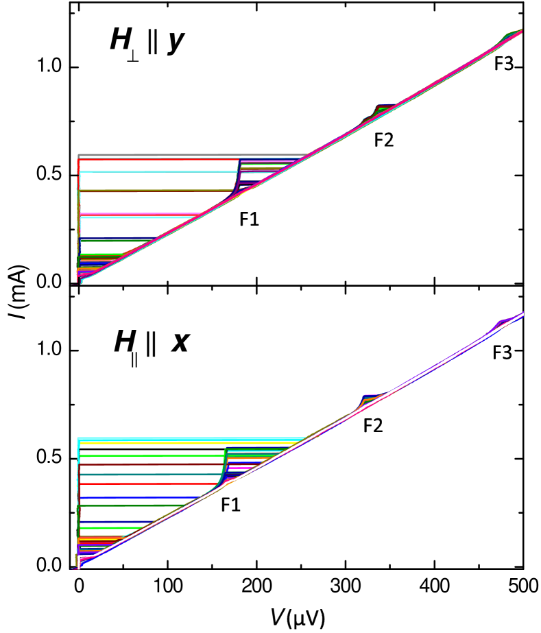
When analyzing the voltage position of the Fiske resonances in detail we have to take into account the idle region next to the junction area. As discussed above, this idle region results in an increase or decrease of the phase velocity compared to the Swihart velocity of an ideal junction without any idle region, depending on whether the idle region is lateral or longitudinal, respectively. In turn, this causes an increase or decrease of the characteristic voltages . For , the resonant modes are extending in -direction, that is, parallel to the idle region (lateral mode). In this case the effect on the phase velocity is described by eq(9) and we expect a slight increase of and . Analogously, for the resonant modes are extending in -direction, that is, perpendicular to the idle region (longitudinal mode). In this case, the effect on the phase velocity is described by eq(10) and we expect a slight decrease of and . This is in good qualitative agreement with our experimental observation. For , resonant modes are found at V, V, V, V and V, whereas for the resonant modes appear at slightly larger voltages V, V, V, V and V. We note, that the correction factors estimated from eqs.(9) and (10) indicated an even bigger difference between the lateral and longitudinal mode. However, the quantitative evaluation of this difference depends on the details of the junction geometry and properties of the involved materials (e.g. dielectric constants) and therefore needs a more elaborate effort Lee91 ; IEEEApplSup2Lee . Qualitatively we can say that the effect of the idle region is reduced on going to higher frequencies (smaller wavelengths) due to a stronger confinement of the modes in the junction area. That is, the difference of the resonance voltages of the lateral and longitudinal mode is decreasing on going to higher harmonics. This nicely agrees with our observation and reports in literature Lee91 .
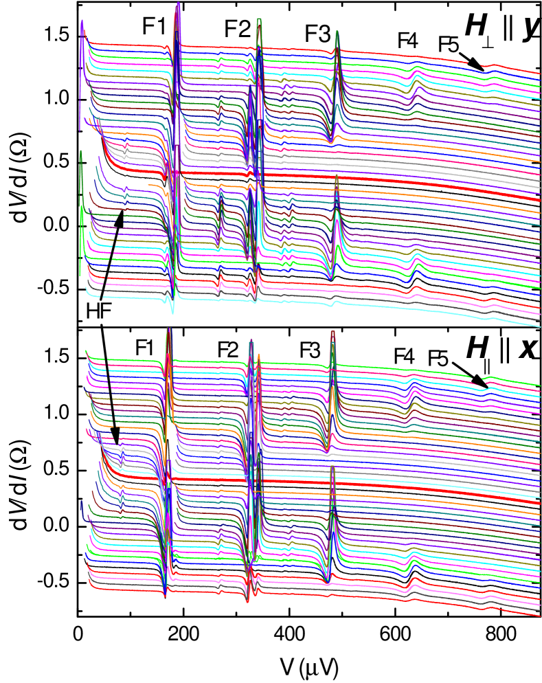
The Fiske steps are obtained from the measured IVCs (cf. Fig. 6) by subtracting an ohmic background which is determined by the about constant subgap resistance. Equivalently, can be obtained by integration of the curves shown in Fig. 7, again after substraction of the subgap resistance. The latter method yields better results for the higher modes. A detailed quantitative description of the voltage position and the shape of the Fiske resonances was given by Kulik for standard SIS Josephson tunnel junctions JETPKulik . In this section we analyze the Fiske steps in the IVCs of our SIFS Josephson junctions using an extension of Kulik’s theory Barone ; Kulik1967 ; Paterno1978 ; PRBGou . According to this theory, the Fiske steps can be expressed as Barone ; Kulik1967
| (15) | |||||
Here, is the quality factor of the -th resonant mode and its voltage position. The function describes the flux dependence of the resonant mode given by
| (16) | |||||
| (17) |
with . The flux dependence of the maximum height of the Fiske steps is given by Barone ; Kulik1967
| (18) |
Fitting the current steps measured at fixed applied flux to (15) allows us to determine the voltage positions () and the maximum step heights () for the magnetic field applied parallel (perpendicular) to the base electrode. For low , the quality factors determined by eq.(18) are not within the validity of Kulik’s theory applicable only for low . Therefore, the the quality factors () listed in Table 2 have been calculated by an extended theory more appropriate for the high- regime Barone .
| number of Fiske step | 1/2 | 1 | 2 | 3 | 4 | 5 |
|---|---|---|---|---|---|---|
| bottom electrode (-direction): | ||||||
| (A) | 140 | 48 | 27 | 13 | 6 | |
| 22 | 27 | 35 | 30 | 22 | ||
| (V) | 83.5 | 167 | 322 | 475 | 630 | 772 |
| bottom electrode (-direction): | ||||||
| (A) | 130 | 46 | 24 | 13 | 5 | |
| 19 | 26 | 31 | 30 | 18 | ||
| (V) | 90.5 | 181 | 336 | 483 | 636 | 780 |
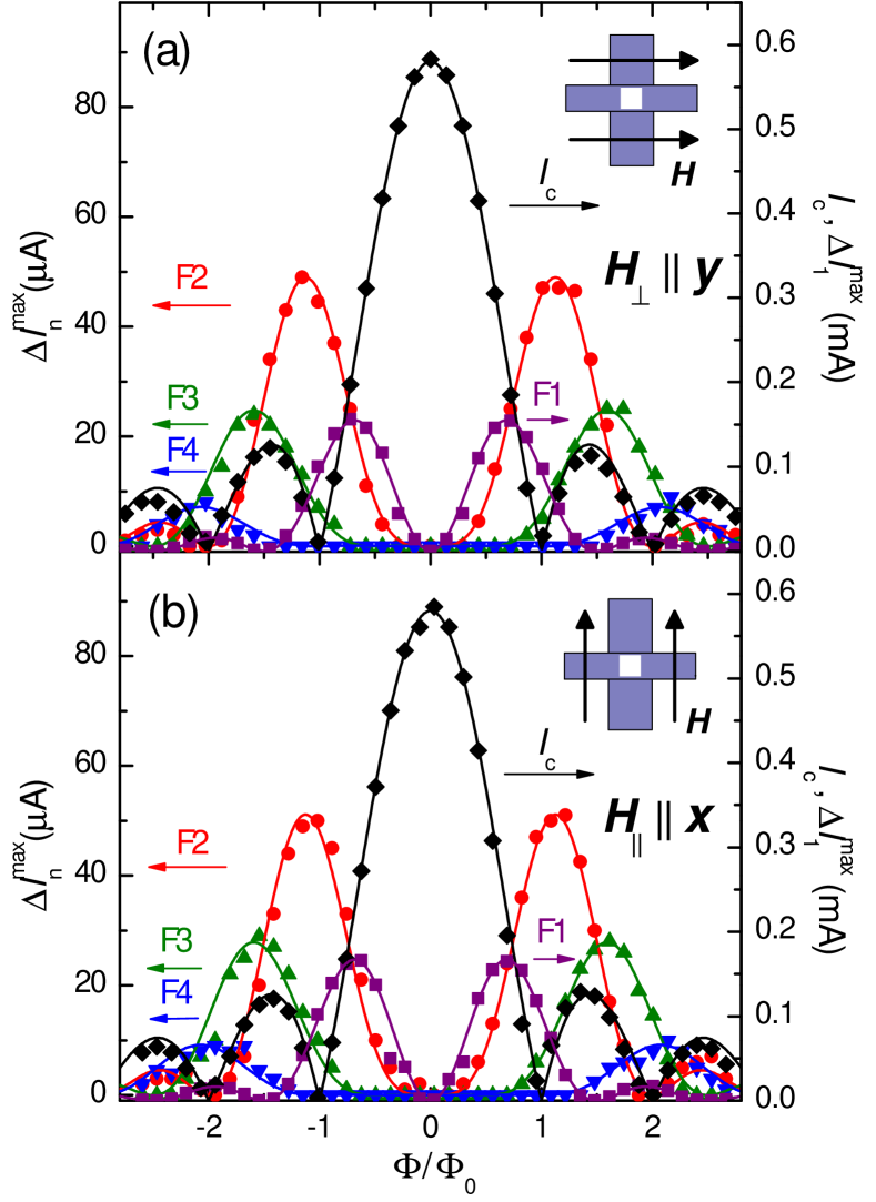
As discussed above, for short Josephson junctions the excitation of the cavity resonances is most effective, if the spatial period of the Josephson current distribution along the junction is about matching the spatial period of the -th resonant electromagnetic mode of the junction. Therefore, the height of the Fiske steps strongly depends on the applied magnetic field and has a pronounced maximum at a particular field value. This is shown in Fig. 8, where we have plotted the height of the -th Fiske step together with the critical current of a junction versus the applied magnetic flux. For large , the Fiske step has a maximum height at where the Josephson current shows about the same spatial modulation along the junction as the cavity mode.
The voltage positions of the Fiske resonances allow us to derive several interesting junction parameters such as the Swihart velocity, the specific capacitance, or the junction plasma frequency. To avoid any ambiguities related to the overlap effect discussed above, we use the Fiske voltages found for to derive these parameters. Obviously, the values directly give the Swihart velocity . From the position V of the first Fiske step we obtain to , where is the speed of light in vacuum. We note that the derived Swihart velocity may slightly vary with increasing step number, e.g. due to a nonvanishing dispersion of the dielectric constant of the barrier material IEEEApplSup2Lee ; PRBHermon . Using the Josephson penetration depth m determined in section 3, the plasma frequency is obtained to 17.8 GHz. Since , we can derive the specific capacitance of the junction to . This value is about two times larger than typical values reported in literature for Nb/AlOx/Nb Josephson junctions APLZant . With these values the quality factor can be estimated, which directly follows from the Swihart velocity derived from the position of the first Fiske resonance. Here, is the resistance of the junction measured at a voltage V corresponding to the plasma frequency. agrees well with the subgap resistance . Using this value we obtain the quality factor , which corresponds to the quality factor determined from the retrapping current of the IVC of the same junction using the RCSJ-model. The fact that is slightly larger than the value is not astonishing keeping in mind effects of premature switching/retrapping due to noise in the IVC measurement. For the junction we observed Fiske resonances at V and V (not shown). Taking into account a slight increase of the first Fiske voltage due to the overlap effect and a decrease of the second due to dispersion effects, we can estimate a Fiske step distance of about V. This value leads to in agreement with the value obtained for the large junction. The derived plasma frequency is GHz and the quality factor is .
We next use the quality factors derived from the Fiske steps to analyze damping effects. In the theoretical description of the Fiske resonances a finite damping is assumed. However, the origin of this damping is usually not specified. It turns out that the experimental values of derived from the Fiske resonances can be both larger and smaller than the quality factor derived from the resistively and capacitively shunted junction (RCSJ) model. The reason is that on the one hand the RCSJ model overestimates the losses due to quasiparticle tunneling, since a voltage independent resistance is assumed in this model. On the other hand, the RCSJ model does not take into account other loss mechanisms, e.g. due to a finite surface resistance. Assuming that there are various loss mechanisms the total quality factor of the Fiske resonances can be written as
| (19) |
Here, the different contributions represent losses due to quasi-particle tunneling () and a finite surface resistance () as well as radiation losses (), and dielectric losses () PRBSmith . Furthermore, variations in the junction length lead to a broadening of the resonances which can be expressed by a frequency independent quality factor .
If quasiparticle tunneling is the only damping mechanism we would expect . Here, is the junction normal resistance at the voltage , which is given by the about constant subgap resistance in the relevant regime. Therefore, is expected to increase about linearly with increasing resonant mode frequency. Above we have determined . Extrapolating the value to larger frequency we would expect . This dependence is shown in Fig. 9 by the broken straight line. Obviously, the quality factors determined from the Fiske resonances do not follow this line. From this we can conclude that there are additional damping mechanisms beside quasiparticle tunneling. In order to get some insight into the frequency dependence of these additional mechanisms, we have used (19) to determine the part in the quality factor due to the additional damping mechanisms by subtracting the quasiparticle damping. The resulting values are shown as open symbols in Fig. 9. It is evident that decreases significantly with increasing frequency.
As discussed above there are several possible mechanisms leading to additional damping in Josephson junctions. However, radiation and dielectric losses usually can be neglected due to the large impedance mismatch at the junction boundaries and the small volume of the dielectric, respectively. Furthermore, in our fabrication process, for resulting in . That is, the geometric inhomogeneities set an upper limit of the quality factor of the junctions, which is above the measured values. The remaining mechanism is damping due to the finite surface resistance of the junction electrodes. Expressing the complex surface impedance of a superconductor as , the contribution of the junction electrodes to the quality factor is given by the ratio PRBBroom
| (20) |
For a rough estimate of we can use a simple two-fluid model. Expressing the conductivity of the superconductor as the sum of the superconducting and normal conducting carriers and using the simple relations Tinkham
| (21) | |||||
| (22) |
we can derive the following expression for the real and imaginary part of the complex surface impedance:
| (23) | |||||
| (24) |
Here, is the temperature dependent fraction of normal electrons, the mass of the normal electrons, and is the conductivity of the superconductor in the normal state where . With these expressions we obtain
| (25) |
We see that increases strongly with decreasing temperature due to the freeze out of the normal electrons. However, due to the uncertainties in , in the PdNi/Nb bilayer, and the simplicity of our approach, eq. (25) certainly cannot be used to estimate the absolute value of . However, according to (25) we expect . This explains the observed decrease of with increasing frequency shown in Fig. 9.
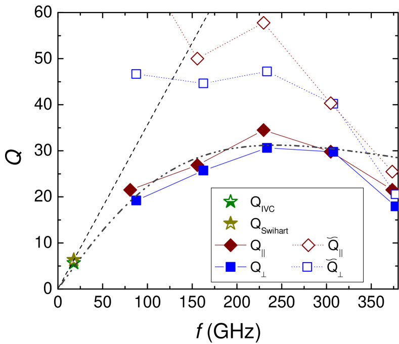
With the quasiparticle tunneling, the finite surface resistance and geometric inhomogeneities as the three main contributions to the measured quality factor, we expect
| (26) |
As shown in Fig. 9, this expression well fits the measured data with , , and . From this we can learn that the quality factor of our SIFS junctions is limited by quasiparticle tunneling at low frequencies and the finite surface resistance at high frequencies. In the intermediate regime there may be an effect of geometric inhomogeneities when going to small area junctions.
The quality factors measured for our SIFS Josephson junctions are slightly lower than the values reported for Nb/AlOx/Nb tunnel junctions IEEEGijsbertsen . This is not astonishing because there is the additional F layer in our SIFS junctions. First this layer reduces the product of the SIFS junction compared to a SIS junction and thereby increases the effect of quasiparticle damping characterized by . Furthermore, the F layer results in an increased surface resistance since the PdNi/Nb bilayer has increased and an increased fraction of the normal electrons. The increased value is a result of the inverse proximity effect, increasing the quasi-particle density in the superconducting electrodes Bergeret2005a . Finally, effects originating from magnetic impurity scattering on Ni atoms diffused into the niobium top layer may play a role Nam:1967 .
Comparing SIFS to SFS junctions, it is immediately evident that the quality factors of SFS junctions will be very small. Due to the much smaller normal resistance and vanishing capacitance, SFS junctions are overdamped (). The larger quality factors of the SIFS junctions are obtained by the additional tunneling barrier, which causes large and . Increasing the thickness of the tunneling barrier is expected to result in an exponential increase of , while should stay constant and should decrease as . Therefore, increasing in principle can be used to further increase the quality factors of SIFS junctions. However, this is obtained at the cost of lower and what may be a problem for some applications. The quality factors between about 5 and 30 in the frequency regime between about 10 and 400 GHz achieved in our experiments are already sufficient for applications in quantum information circuits or for studies of macroscopic quantum tunneling.
We conclude the discussion of Fiske resonances by paying attention to the small resonances labeled HF in Fig. 7, which occur at exactly half of the voltage of the first Fiske step. This observation reminds us of the appearance of half-integer Shapiro steps at the 0--transition of SFS junctions due to a second harmonic component in the current-phase relation PRLSellier . However, since the F layer thickness of the SIFS junctions studied in our work is about twice the thickness of the 0--transition, this scenario would require a significant F layer thickness variation of a few nanometers goldobin2Phi . This is in contradiction to the small rms roughness of our F layers. Furthermore, the presence of a double-sinusoidal current-phase relation as the origin of the HF resonance is in contradiction with the measured magnetic flux dependence of its height. Clearly the measured oscillation period of the HF resonance cannot be mapped on twice the period of the first Fiske step Biedermann1997 . Nonequilibrium effects may be a possible explanation for the observed HF resonance Argaman1999 . However, further experiments are required to clarify this point.
5 Conclusion
We have fabricated Nb/AlOx//Nb (SIFS) Josephson junctions with controllable and reproducible properties using a self-align process. High current densities up to more than A/cm2 and values above have been achieved. The dependencies are close to an ideal Fraunhofer diffraction pattern demonstrating the good spatial homogeneity of the junctions. The transition from - to -coupled junctions was observed for a thickness nm of the layer. The layers show an out-of-plane anisotropy. They have a Curie temperature of 150 K, an exchange energy meV, and a saturation magnetization of about per Ni atom, indicating that there are negligible magnetic dead layers at the interfaces. The dependence of the SIFS junctions can be well described by the dirty limit theory of Buzdin et al. BuzdinPRB2003 yielding the single characteristic length scale nm for the decay and oscillation of the critical current. From the measured IVCs and the Fiske resonances appearing at finite applied magnetic flux the junction quality factor has been determined in the wide frequency range between about 10 and 400 GHz. At low frequencies the quality factor increases about linearly with frequency due to the about frequency independent damping related to quasiparticle tunneling, whereas it decreases proportional to at high frequencies due to the increasing surface resistance of the junction electrodes. The achieved quality factors range between about 5 at the junction plasma frequency and 30 at about 200 GHz and are sufficient for applications of SIFS junctions in superconducting quantum circuits or experiments on macroscopic quantum tunneling.
Acknowledgements.
We gratefully acknowledge financial support by the Deutsche Forschungsgemeinschaft via SFB 631 and the German Excellence Initiative via the Nanosystems Initiative Munich (NIM). We thank M. Weides and J. Pfeiffer for fruitful discussions as well as Th. Brenninger for technical support.References
- (1) P. Fulde, R.A. Ferrell, Phys. Rev. 135(3A), A550 (1964)
- (2) A.I. Larkin, Y.N. Ovchinnikov, Zh. Eksp. Teor. Fiz. 47, 1136 (1964)
- (3) L.N. Bulaevskii, V.V. Kuzii, A.A. Sobyanin, JETP Lett. 25(25), 290 (1977)
- (4) A.I. Buzdin, Rev. Mod. Phys. 77(3), 935 (2005)
- (5) A. Buzdin, L. Bulaevskii, S. Panyukov, JETP Lett. 35(4), 178 (1982)
- (6) A.I. Buzdin, B. Vujicic, M. Kupriyanov, JETP 74, 124 (1992)
- (7) J.S. Jiang, D. Davidović, D.H. Reich, C.L. Chien, Phys. Rev. Lett. 74(2), 314 (1995)
- (8) V.V. Ryazanov, V.A. Oboznov, A.Y. Rusanov, A.V. Veretennikov, A.A. Golubov, J. Aarts, Phys. Rev. Lett. 86(11), 2427 (2001)
- (9) T. Kontos, M. Aprili, J. Lesueur, F. Genet, B. Stephanidis, R. Boursier, Phys. Rev. Lett. 89(13), 137007 (2002)
- (10) H. Sellier, C. Baraduc, F. Lefloch, R. Calemczuk, Phys. Rev. B 68(5), 054531 (2003)
- (11) V. Ryazanov, V. Oboznov, A. Prokofiev, V. Bolginov, A. Feofanov, J. Low. Temp. Phys. 136(5), 385 (2004)
- (12) V.A. Oboznov, V.V. Bol’ginov, A.K. Feofanov, V.V. Ryazanov, A.I. Buzdin, Phys. Rev. Lett. 96(19), 197003 (2006)
- (13) J.Y. Gu, C.Y. You, J.S. Jiang, J. Pearson, Y.B. Bazaliy, S.D. Bader, Phys. Rev. Lett. 89(26), 267001 (2002)
- (14) E.A. Demler, G.B. Arnold, M.R. Beasley, Phys. Rev. B 55(22), 15174 (1997)
- (15) A. Buzdin, I. Baladié, Phys. Rev. B 67(18), 184519 (2003)
- (16) F.S. Bergeret, A.F. Volkov, K.B. Efetov, Phys. Rev. B 68(6), 064513 (2003)
- (17) F.S. Bergeret, A.F. Volkov, K.B. Efetov, Phys. Rev. B 75(18), 184510 (2007)
- (18) M. Fauré, A.I. Buzdin, A.A. Golubov, M.Y. Kuprianov, Phys. Rev. B 73(6), 064505 (2006)
- (19) W. Guichard, M. Aprili, O. Bourgeois, T. Kontos, J. Lesueur, P. Gandit, Phys. Rev. Lett. 90(16), 167001 (2003)
- (20) Y. Blum, A. Tsukernik, M. Karpovski, A. Palevski, Phys. Rev. Lett. 89(18), 187004 (2002)
- (21) A. Bauer, J. Bentner, M. Aprili, M.L. Della Rocca, M. Reinwald, W. Wegscheider, C. Strunk, Phys. Rev. Lett. 92(21), 217001 (2004)
- (22) S.M. Frolov, D.J. Van Harlingen, V.A. Oboznov, V.V. Bolginov, V.V. Ryazanov, Phys. Rev. B 70(14), 144505 (2004)
- (23) J.W.A. Robinson, S. Piano, G. Burnell, C. Bell, M.G. Blamire, Phys. Rev. Lett. 97(17), 177003 (2006)
- (24) M. Weides, M. Kemmler, E. Goldobin, D. Koelle, R. Kleiner, H. Kohlstedt, A. Buzdin, Appl. Phys. Lett. 89(12), 122511 (2006)
- (25) J. Pfeiffer, M. Kemmler, D. Koelle, R. Kleiner, E. Goldobin, M. Weides, A.K. Feofanov, J. Lisenfeld, A.V. Ustinov, Phys. Rev. B 77(21), 214506 (2008)
- (26) I. Petkovic, M. Aprili, Phys. Rev. Lett. 102(15), 157003 (2009)
- (27) T.S. Khaire, W.P. Pratt, N.O. Birge, Phys. Rev. B 79(9), 094523 (2009)
- (28) A. Buzdin, A. Koshelev, Phys. Rev. B 67(22), 220504 (2003)
- (29) M. Weides, M. Kemmler, H. Kohlstedt, R. Waser, D. Koelle, R. Kleiner, E. Goldobin, Phys. Rev. Lett. 97(24), 247001 (2006)
- (30) M. Weides, C. Schindler, H. Kohlstedt, J. Appl. Phys. 101(6), 063902 (2007)
- (31) T.P. Orlando, J.E. Mooij, L. Tian, C.H. van der Wal, L.S. Levitov, S. Lloyd, J.J. Mazo, Phys. Rev. B 60(22), 15398 (1999)
- (32) I. Chiorescu, Y. Nakamura, C. Harmans, J. Mooij, Science 299, 1869 (2003)
- (33) F. Deppe, M. Mariantoni, E.P. Menzel, S. Saito, K. Kakuyanagi, H. Tanaka, T. Meno, K. Semba, H. Takayanagi, R. Gross, Phys. Rev. B 76(21), 214503 (2007)
- (34) F. Deppe, M. Mariantoni, E.P. Menzel, A. Marx, S. Saito, K. Kakuyanagi, T. Meno, K. Semba, H. Takayanagi, E. Solano et al., Nature Physics 4, 686 (2008)
- (35) T. Niemczyk, F. Deppe, M. Mariantoni, E. Menzel, E. Hoffmann, G. Wild, L. Eggenstein, A. Marx, R. Gross, Supercond. Sci. Technol. 22, 034009 (2009)
- (36) T. Niemczyk, F. Deppe, H. Huebl, E. Menzel, F. Hocke, M. Schwarz, J.J. Garcia-Ripoll, D. Zueco, T. Hümmer, E. Solano et al., Nature Physics advance online publication (2010)
- (37) G. Blatter, V.B. Geshkenbein, L.B. Ioffe, Phys. Rev. B 63(17), 174511 (2001)
- (38) T. Yamashita, K. Tanikawa, S. Takahashi, S. Maekawa, Phys. Rev. Lett. 95(9), 097001 (2005)
- (39) T. Yamashita, S. Takahashi, S. Maekawa, Appl. Phys. Lett. 88(13), 132501 (2006)
- (40) L.B. Ioffe, V.B. Geshkenbein, M.V. Feigel’man, A.L. Fauchere, G. Blatter, Nature 398(6729), 679 (1999)
- (41) A.K. Feofanov, V.A. Oboznov, V.V. Bol’ginov, J. Lisenfeld, S. Poletto, V.V. Ryazanov, A.N. Rossolenko, M. Khabipov, D. Balashov, A.B. Zorin et al., Nature Physics 6, 597 (2010)
- (42) T. Kato, A.A. Golubov, Y. Nakamura, Phys. Rev. B 76(17), 172502 (2007)
- (43) A. Ruotolo, C. Bell, C.W. Leung, M.G. Blamire, J. App. Phys. 96(1), 512 (2004)
- (44) J. Cable, H. Child, Phys. Rev. B 1(9), 3809 (1970)
- (45) T. Kontos, M. Aprili, J. Lesueur, X. Grison, Phys. Rev. Lett. 86(2), 304 (2001)
- (46) D.H. Dye, S.A. Campbell, G.W. Crabtree, J.B. Ketterson, N.B. Sandesara, J.J. Vuillemin, Phys. Rev. B 23(2), 462 (1981)
- (47) C. Cirillo, S.L. Prischepa, M. Salvato, C. Attanasio, M. Hesselberth, J. Aarts, Phys. Rev. B 72(14), 144511 (2005)
- (48) Tinkham, Introduction to superconductivity (McGraw-Hill, New York, 1996)
- (49) H. Kohlstedt, A. Ustinov, F. Peter, IEEE Trans. Appl. Sup. 5(2), 2939 (1995)
- (50) J.C. Swihart, J. Appl. Phys. 32(3), 461 (1961)
- (51) M. Weihnacht, phys. stat. sol. (b) 32(2), K169 (1969)
- (52) D.D. Coon, M.D. Fiske, Phys. Rev. 138(3A), A744 (1965)
- (53) G. Lee, IEEE Trans. Appl. Sup. 1(3), 121 (1991)
- (54) G. Lee, A. Barfknecht, IEEE Trans. Appl. Sup. 2(2), 67 (1992)
- (55) R. Monaco, G. Costabile, N. Martucciello, J. Appl. Phys. 77(5), 2073 (1995)
- (56) W.C. Stewart, Appl. Phys. Lett. 12(8), 277 (1968)
- (57) R. Gross, D. Koelle, Rep. Prog. Phys. 57(7), 651 (1994)
- (58) J. Bosch, R. Gross, M. Koyanagi, R.P. Huebener, Phys. Rev. Lett. 54(13), 1448 (1985)
- (59) G.M. Fischer, B. Mayer, R. Gross, T. Nissel, K.D. Husemann, R.P. Huebener, T. Freltoft, Y. Shen, P. Vase, Science 263(5150), 1112 (1994)
- (60) R. Gerdemann, K.D. Husemann, R. Gross, L. Alff, A. Beck, B. Elia, W. Reuter, M. Siegel, J. Appl. Phys. 76(12), 8005 (1994)
- (61) M. Weides, Appl. Phys. Lett. 93, 052502 (2008)
- (62) B.D. Josephson, Phys. Lett. 1(7), 251 (1962)
- (63) M.D. Fiske, Rev. Mod. Phys. 36(1), 221 (1964)
- (64) A. Barone, G. Paterno, Physics and applications of the Josephson effect (John Wiley & Sons, Inc., 1982)
- (65) I. Kulik, JETP Lett. 2, 84 (1965)
- (66) I. Kulik, Sov. Phys. Tech. Phys. 12(1), 111 (1967)
- (67) G. Paterno, J. Nordman, J. Appl. Phys. 49(4), 2456 (1978)
- (68) Y.S. Gou, R.I. Gayley, Phys. Rev. B 10(11), 4584 (1974)
- (69) Z. Hermon, A. Stern, E. Ben-Jacob, Phys. Rev. B 49(14), 9757 (1994)
- (70) H.S.J. van der Zant, R.A.M. Receveur, T.P. Orlando, A.W. Kleinsasser, Appl. Phys. Lett. 65(16), 2102 (1994)
- (71) H.J.T. Smith, Phys. Rev. B 24(1), 190 (1981)
- (72) R. Broom, P. Wolf, Phys. Rev. B 16(7), 3100 (1977)
- (73) J. Gijsbertsen, E. Houwman, J. Flokstra, H. Rogalla, J. le Grand, P. de Korte, IEEE Trans. Appl. Sup. 3(1), 2100 (1993)
- (74) F.S. Bergeret, A.L. Yeyati, A. Mart n-Rodero, Phys. Rev. B 72(6), 064524 (2005)
- (75) S. Nam, Phys. Rev. 156(2), 487 (1967)
- (76) H. Sellier, C. Baraduc, L. Francois, R. Calemczuk, Phys. Rev. Lett. 92(25), 257005 (2004)
- (77) E. Goldobin, D. Koelle, R. Kleiner, A. Buzdin, Phys. Rev. B 76(22), 224523 (2007)
- (78) K. Biedermann, A. Chrestin, T. Matsuyama, U. Merkt, Appl. Sup. 5, 255 (1997)
- (79) N. Argaman, Superlatt. Microstruct. 25(5-6), 861 (1999)