Electronic fiber in graphene
Abstract
We investigate theoretically the transmission properties through a p-n-p junction on graphene. Here we show that the electronic transport property presents deep analogies with light propagation. It originates from the similarity between the linear spectrum of the Dirac fermions and photons that obey the Maxwell’s equations. We demonstrate the p-n-p channel acts as an electronic fiber in which electrons propagate along the channel without dissipation.
pacs:
73.22.-f 73.23.-b 73.40.Gk 85.30.DeIn recent years, graphene, a single layer of carbon atoms arranged in a hexagonal lattice, exhibits abundant physics and potential applications. Novoselov2 ; Zhang ; Novoselov1 ; Geim ; Neto Quantum transport properties in graphene have attracted increasing attentions both from the fundamental physics and potential application in carbon-based nano-electronics devices. The properties arise from the unique linear energy dispersion and the chiral nature of electrons at the () point of the Brillouin zone, the energy spectrum exhibits a linear dispersion that can be well described by the massless Dirac equation. Neto These massless Dirac fermions, can be viewed as electrons that lose their rest mass , or as neutrinos that acquire the electron charge . Electrons in graphene are quite different from the electrons in conventional semiconductor two dimensional electron gases.
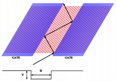
Dirac equation describing the motion of massless quasiparticles is mathematically similar to the Helmholz equation for an electromagnetic wave. Graphene nano structures have been achieved by lithography as small as few nanometers. Ozyilmaz While, the mean-free path of electron in graphene approaches the order of micron at room temperature, Geim and the electron wavelength is even lager. Morozov In such ballistic regime, the scattering of electrons by potential barriers can be understood by comparing with the reflection, refraction and transmission of electromagnetic waves in inhomogeneous media. So, graphene monolayer is a suitable candidate to examine the optical-like phenomena of the Dirac fermions, that have attracted a lot of interest, Cheianov ; Jr ; Park ; FMZhang ; Darancet ; Beenakker ; Ghosh ; Zhao ; Concha such as waveguide, Goos-Hnchen effect, Beenakker Bragg reflection, coherent buffers/memories, and Brewster-type angle in graphene. Note that it was clearly demonstrated by Cheianov et al. Cheianov that graphene based n-p-n junctions could be used as electronic lenses or beam splitters. In this letter, we investigated theoretically transport property of Dirac electrons in a p-n-p channel created by two electrostatic gates that are deposited on top of the graphene monolayer (see Fig. 1). The transport process along the channel determined by the multiple total internal reflection. We find that in such a p-n-p channel, electrons can be confined in between two interfaces, in analogy with the light propagation in an optical fiber. In addition, the approach presented in this work could also be applied directly to electronic excitations in another recently hotspot material, namely the topological insulator that also has Dirac cones. Qi ; LBZhang

Model—Tunable potential barriers could be created on a single-layer graphene sheet, Huard ; Williams by electrostatic gates deposited on top or back of the graphene monolayer. The electrostatic potentials can be tuned by changing applied voltages (see Fig. 1). The low-energy electrons near the point of the Dirac cones can be well described by the effective Hamiltonian Wallace
| (1) |
where the superscript indicates the -th region, is the Fermi velocity, is the Pauli matrix and is the height of the electrostatic barrier. The wavevector satisfies . Note that the translational invariance along the y direction gives rise to the conservation of , and thus the solutions can be written as . For brevity, we will set in the follows.

Refraction and total reflection—We started by investigating electron tunneling through an electric p-n junction on graphene, with in the n-doped region and in the p-doped region. This requirement fixes the dependence of the longitudinal outgoing wave vector . Note that, when , denotes the interband scattering at the interface of the p-n junction which is required by the helicity nature of the Dirac Fermions. Continuity of the wave functions at gives the transmission coefficient: Since the modes in n-doped and p-doped regions have different group velocities, the transmission probability is given by , where for propagating states and for evanescent states. This expression has the advantage that can well describe the propagating states and evanescent states in a unified form. We can also define the incident and refractive angles for electrons in propagating states , and , and rewrite the transmission probability as
| (2) |
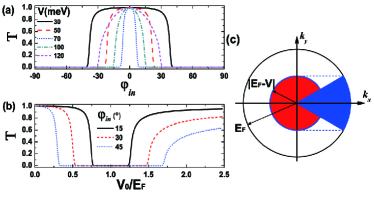
This is valid for incident angle , and the Heaviside step function guarantees a general expression of the transmission probability whether interband scattering occurs or not. is analogy to critical angle for total reflection in optics and gives the Snell’s law for transmitted electrons. It shows that the effective Fermi energy () plays the role of index of refraction in optical medium. Note that when , refractive index of graphene is negative as a metamaterial. In this case, electrons are injected to the hole branch in p region, the chirality of Dirac electrons in graphene gives rise to sign reversal of the momentum of the forward-going state. Importantly, one can tune the refractive index in quite a large range via electrostatic gates, which is not easy for normal metamaterials. We note en passant that such optic-like behaviours are absent in the tunneling through a barrier, Chen since the effective Fermi energies at both side of the barrier are , indicating an identical index of refraction.
The transmission spectra for electrons traversing such a p-n junction are shown in Fig. 2(a) and (b), which can be understood from the phase diagram of Fig. 2(c). For a fixed incident energy, the transmission declines sharply and then is blocked when the incident angle exceeds a critical value (see Fig. 2(a)), while the wavevector in the p-doped region become imaginary denoting the appearance of evanescent modes. The critical angle for total reflection can be estimated by the Snell’s law, . The transmission can also be tuned by the gate voltage, or equivalently, the barrier height (see Fig. 2(b)). A transmission gap appears as the gate voltage approaching the incident energy and become wider as increasing the incident angle . These tunneling features are well appreciated by inspecting the phase diagram as shown in Fig. 2(c). The Fermi wavevector is different in n-doped and p-doped region as a consequence of gate voltage , i.e., , , while the component is conserved. The requirement leads to non-zero transmission for allowed incident angles as a sector in Fig. 2(c) in accordance with our numerical results in Fig. 2(a). It is clear that declines as the gate voltage approaching the incident energy , so transmission gaps appear when drops below that verifies the calculation as shown in Fig. 2(b).


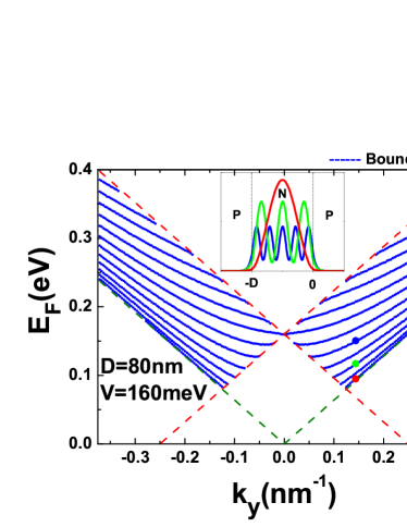
Fiber guiding–We considered an electric p-n-p channel with width (see Fig.1) and focus on the electrons transporting along the interface rather than across it. The transmission gap discussed above can lead to confinement of electrons between the two interfaces associated with multiple total internal reflections. Electrons can transport along the p-n-p channel just like photons in an optical fiber. We calculated the energy dispersion relation of the bound states in the case of total internal reflection at both two interfaces (i.e. , is imaginary). Matching of propagating waves to evanescent waves at and , the energy spectrum of the bound states can be obtained from the zero point of the determinant of the coefficients, which can be reduced to a transcendental equation
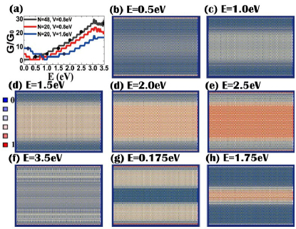
The energy spectrum is plotted for the first few bound states in Fig. 3. The dashed lines , and give the boundary that delimit the continuum region, corresponding to propagating states in x-direction. Confinement of electrons in x-direction gives rise to non-dispersive transporting in y-direction. The bound states between the two interfaces thus play the roles of guide modes along the channel that can effectively convey the charge carriers with group velocities indicated by the slope of the dispersion relation. The spectrum is symmetric with respect to the transverse wave vector , guaranteed by the time reversal symmetry. So the transport properties is isotropic for each incident terminal. The inset of Fig. 3 shows the probability density of the bound states marked by the solid circular dot. The vertical dashed lines indicate the interfaces of the p-n-p junction. It is clear that the solutions are standing waves in the channel and decay exponentially in the barrier regions. Note that the order of the bound states equals to the number of peaks of standing waves in the channel, e.g. the 1st, 3rd and 5th bound states or guide modes are shown in the inset of Fig. 3. Thus, the bound states serve as guide modes in cavity. Finally, we focused on how the fiber guiding features shown above are reflected in the measurable quantity, the conductance . We performed numerical simulations of electrical conduction in a tight-binding model of a graphene zigzag ribbon covered by electrodes. The conductance is evaluated using the recursive Green function technique and Landauer-Büttiker formula. The conductance of the gated ribbon displays a step-like feature, which corresponds to the opening of the new modes as the Fermi energy increases (see Fig. 4(a)). When is very small, there is no bound states in the channel, the conductance is contributed by the edge states of the zigzag ribbon, since our simulation are performed in a lattice scale. In such low incident energy region, the conductance for a thinner channel may also depend on the former hole-branch bulk states that are lifted up to the Fermi energy by the gate voltage. A lager gate voltage can make this effect more pronounced. When the incident Fermi energy lays in an interval around the gate voltage, electrons could be totally reflected with a small enough critical angle since there exist a great difference between the refraction indexes at two sides of the interface. In this case, most transmission modes are formed by the bound states in the channel and desired high effective fiber guiding is obtained. As the Fermi energy is increased continuously, the refraction indexes of the channel and the gated region approach to each other gradually, so the total reflection critical angle becomes very large. Electrons can leak out of the channel easily, leading to decrease of guide efficiency. This is because the transmission modes are mixture of both bound states and bulk states out of the channel. Above expectations are demonstrated by examining the electron density distributions as shown in Fig. 4(b)-(h)). It is apparent that electrons are mainly distributed in the channel when the incident Fermi energy is around the gate voltage and thus the conductance depends on the guide modes by virtue of the gate voltage and channel width. In addition, similar results could be obtained when the gate voltage or incident energy are minus due to the particle-hole symmetry.
In summary, We investigate theoretically the electronic quantum transport properties in a p-n-p junction on graphene. Our results demonstrate that the proposed structure on graphene presents deep analogies with optic phenomena as refraction and total internal reflection. The quantized dispersion relation of the confined electron states are obtained in our calculation. We show that these bound states serve as guide modes and can carry current along the channel with out radiation. The investigation could be helpful to offer a functionality of graphene based electronic fiber.
References
- (1) K. S. Novoselov, A. K. Geim, S. V. Morozov, D. Jiang, Y. Zhang, S. V. Dubonos, I. V. Grigorieva, and A. A. Firsov, Science 306, 666 (2004).
- (2) Y. Zhang, Y. Tan, H. L. Stormer, and P. Kim, Nature 438, 201 (2005).
- (3) K. S. Novoselov, Z. Jiang, Y. Zhang, S. V. Morozov, H. L. Stormer, U. Zeitler, J. C. Maan, G. S. Boebinger, P. Kim, and A. K. Geim, Science 315, 1379 (2007).
- (4) A. K. Geim, and K. S. Novoselov, Nature Mater. 6, 183 (2007).
- (5) A. H. Castro Neto, F. Guinea, N. M. R. Peres, K. S. Novoselov, and A. K. Geim, Rev. Mod. Phys. 81, 109 (2009).
- (6) B. Özyilmaz, P. Jarillo-Herrero, D. Efetov, D. A. Abanin, L. S. Levitov, and P. Kim, Phys. Rev. Lett. 99, 166804 (2007).
- (7) S. V. Morozov, K. S. Novoselov, M. I. Katsnelson, F. Schedin, D. C. Elias, J. A. Jaszczak, and A. K. Geim, Phys. Rev. Lett. 100, 016602 (2008).
- (8) V. V. Cheianov, V. Fal’ko, and B. L. Altshuler, Science 315, 1252 (2007).
- (9) J. Milton Pereira. Jr., V. Mlinar, and F. M. Peeters, Phys. Rev. B 74, 045424 (2006).
- (10) C. H. Park, Y. W. Son, L. Yang, M. L. Cohen, and S. G. Louie, Nano Lett. 8, 2920 (2008).
- (11) F. M. Zhang, Y. He, and Xi. Chen, Appl. Phys. Lett. 94 212105 (2009).
- (12) P. Darancet, V. Olevano, and D. Mayou, Phys. Rev. Lett. 102, 136803 (2009).
- (13) C. W. J. Beenakker, R. A. Sepkhanov, A. R. Akhmerov, and J. Tworzydlo, Phys. Rev. Lett. 102, 146804 (2009).
- (14) S. Ghosh and M. Sharma, J. Phys.: Condens. Matter 21, 292204 (2009).
- (15) L. Zhao, and S. F. Yelin, Phys. Rev. B 81, 115441 (2010).
- (16) A. Concha and Z. teanovi, Phys. Rev. B 82, 033413 (2010).
- (17) X. L. Qi and S. C. Zhang, Physics Today 63(1), 33 (2010), M. Z. Hasan and C. L. Kane, Rev. Mod. Phys. 82, 3045 (2010).
- (18) For the optic-like transmission behaviors in topological insulators, see, e.g., L. B. Zhang et al. Phys. Rev. B 81 235323 (2010); L. B. Zhang et al. New J. Phys. 12, 083058 (2010); L. B. Zhang et al. Phys. Rev. B 83 081402(R) (2011).
- (19) B. Huard, J. A. Sulpizio, N. Stander, K. Todd, B. Yang, and D. Goldhaber-Gordon, Phys. Rev. Lett. 98, 236803 (2007).
- (20) J. R. Williams, T. Low, M. S. Lundstrom, and C. M. Marcus, Nature Nanotech. advance online publication (13 February 2011). DOI: 10.1038/NNANO.2011.3.
- (21) P. R. Wallace, Phys. Rev. 71, 622 (1947).
- (22) X. Chen and J. W. Tao, Appl. Phys. Lett. 94 262102 (2009).