Fundamental Behavior of Electric Field Enhancements in the Gaps Between Closely Spaced Nanostructures
Abstract
We demonstrate that the electric field enhancement that occurs in a gap between two closely spaced nanostructures, such as metallic nanoparticles, is the result of a transverse electromagnetic waveguide mode. We derive an explicit semianalytic equation for the enhancement as a function of gap size, which we show has a universal qualitative behavior in that it applies irrespective of the material or geometry of the nanostructures and even in the presence of surface plasmons. Examples of perfect electrically conducting and Ag thin-wire antennas and a dimer of Ag spheres are presented and discussed.
pacs:
78.67.-n, 62.23.Hj, 42.25.Fx, 42.25.GyStructures that generate large electric field enhancements relative to the incident field, hereon referred to as enhancements, have recently received a great deal of attention Moskovits (1985); García-Vidal and Pendry (1996); Schuck et al. (2005); Mühlschlegel et al. (2005); Kang et al. (2009); Wustholz et al. (2010); Hao and Schatz (2004); Aizpurua et al. (2005); Romero et al. (2006); Kottmann and Martin (2001). This is because such enhancements are central to a number of physical processes, including such surface-enhanced spectroscopy techniques as surface-enhanced Raman scattering (SERS), second harmonic generation, and enhanced absorption and fluorescence Moskovits (1985). Often the enhanced field is generated in the small crevices of a roughened metal surface García-Vidal and Pendry (1996) or at the junctions of closely spaced nanoparticles Schuck et al. (2005); Mühlschlegel et al. (2005); Kang et al. (2009); Wustholz et al. (2010); Hao and Schatz (2004); Aizpurua et al. (2005); Romero et al. (2006); Kottmann and Martin (2001). Herein we focus on the latter structures, and while much is known about the enhancements in them, there is still confusion over fundamental principles. In particular, the functional dependence on gap size Schuck et al. (2005); Kang et al. (2009); Aizpurua et al. (2005); Romero et al. (2006), arguably the most basic and important aspect, has not been quantitatively determined and the underlying physical principles which determine it are not entirely known. It is the purpose of this Letter to resolve this issue through finite element method (FEM) calculations Jin (2002) and an analytical theory developed for the transmission of light through an isolated slit in a metal film Bravo-Abad et al. (2004).
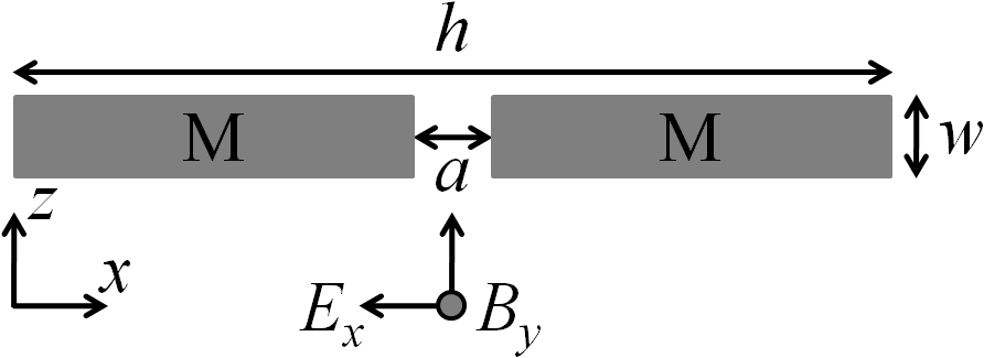
For two closely spaced nanostructures, the enhancements in the resulting gap can in principle be explained using antenna theory Kraus and Marhefka (2001); Pohl (2000), where the open-circuit voltage across the gap is responsible, and thus the systems are often classified as such Schuck et al. (2005); Mühlschlegel et al. (2005). We therefore begin by considering a two-dimensional (2D) antenna as shown schematically in Fig. 1.

[The extension to three dimensions (3D) will be discussed below.] Two metal wires M with widths are separated by a distance and the entire structure spans a length of . The structure is illuminated from below at normal incidence by a plane wave with wavelength , and we wish to determine how the enhancement at the center of the gap depends on . It is important to realize that for a real metal and distances less than approximately nm, nonlocal dielectric effects will become important McMahon et al. (2009). Our quantitative analysis herein will therefore be for nm, but in most cases we will include smaller distances to highlight qualitative features. Antenna theory for a perfect electrically conducting (PEC) thin-wire antenna () assumes that the incident electric field generates an alternating current along , which results in an induced voltage across . If , where is an integer, the antenna resonates and , where is the amplitude of the incident field Kraus and Marhefka (2001). As a result, the open-circuit voltage in the gap should produce a uniform enhancement of .
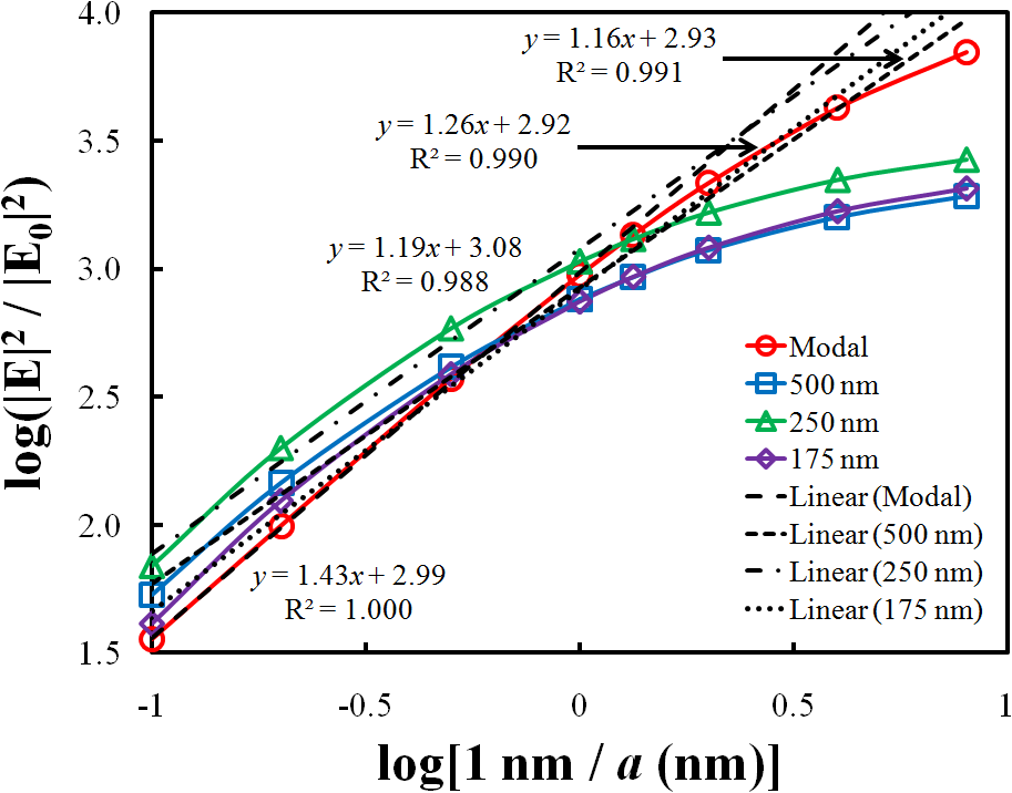
In order to test the above analysis, we rigorously determined the enhancements via FEM calculations Jin (2002) for and nm thin-wire antennas ( and , respectively) with nm at nm for gap sizes of to nm. To characterize the dependence, we can assume that is proportional and plot the results on a log-log scale to determine ; Fig. 2.

For both antennas it is found that for nm, and it is even less for smaller , which is much lower than the above antenna theory prediction of . An alternative way to describe these systems and the enhancements that they exhibit is therefore needed.
The system in Fig. 1 can be greatly simplified by taking , which below we will show does not significantly affect the behavior of the electric field E in the gap. Maxwell’s equations can be solved analytically for such a system (if the metal is a PEC), which is an isolated slit in a metal film, by appropriately expanding the transverse component of the field (the component of the magnetic field, in this case) above and below the film and inside of the gap in terms of known functions and applying boundary conditions at the interfaces. While the full solution for this problem has been implicitly worked out in terms of a system of linear equations Bravo-Abad et al. (2004), we demonstrate that under a few reasonable approximations it is possible to obtain a tractable semianalytical form for .
Inside the gap E can be defined entirely in terms of its component (below we will show that the component is zero), which can be expanded as a superposition of forward and backwards propagating (and evanescent) waveguide modes ,
| (1) |
where and are the respective modal amplitudes, , , and is the solution to the Helmholtz equation subject to PEC boundary conditions on the gap sides at . and can be found by ensuring the continuity of Eq. (1) at the input () and output () surfaces of the gap,
| (2) |
| (3) |
where and are intensities of scattering events that take place at each of the surfaces, which can be determined by solving a set of linear equations (see below) Bravo-Abad et al. (2004).
Inside a gap that is small relative to the incident wavelength (), the only waveguide mode that can exist is the transverse electromagnetic (TEM) one Jackson (1998). In this case, there is no dependence in , is zero, , and the linear equations defining and simplify considerably,
| (4) |
| (5) |
where (for normal incident light) is the overlap amplitude of the incident field with the TEM mode, is the admittance amplitude, is the coupling amplitude between and , and
| (6) |
is the amplitude of the TEM mode’s self-interaction, where is the 2D vacuum Green’s function with being a Hankel function of the first kind. The maximum value that can take is . Since , we can make the small-argument approximation in and perform the integral in Eq. (6) analytically,
| (7) |
where with being Euler’s constant.
For a gap with a small width relative to the incident wavelength () we can use the small-angle approximation in Eqs. (2) and (3) to greatly simplify Eq. (1),
| (8) |
Note that the approximation was also used to get Eq. (8), which is valid considering that the leading terms are and , respectively.
At the center of the gap () Eq. (8) simplifies even further,
| (9) |
where . Equation (9) shows that at the center of the gap E is inversely proportional to the interference between two terms, the self-interaction term , which depends only on , and a term representing the interference between surfaces and , which depends only on .
Using the explicit expressions for and in Eq. (9) and calculating gives
| (10) |
For gaps with not very small relative to (greater than approximately nm for the thin-wire antennas discussed above), E depends primarily on and . Because the enhancement is of the form , we would expect a fit to not work at all. However, over a couple order of magnitude range of values is well-approximated by , where and are constants that can be determined by demanding that this equality and a corresponding one involving its derivative be satisfied at some value of . With these constraints one finds that , which varies slowly with . For nm and nm, and therefore , which is consistent with found for the thin-wire antennas in Fig. 2. For small gaps both and go to zero, which means that E depends primarily on and . Therefore, for we expect a turnover to a weaker dependence, which is also consistent with the results in Fig. 2. Actual enhancements calculated using Eq. (10) for to nm, nm, and nm are shown in Fig. 2 as well, and are in agreement with these remarks.
The strong agreement between the modal and thin-wire antenna results in Fig. 2 suggests that the enhancements in both cases arise from the same effect, a TEM waveguide mode. The former does show a slightly stronger dependence, but this can be understood as follows. Recall that the amplitude for coupling incident light into this mode is proportional to their overlap; see Eq. (4). In a finite structure, such as a thin-wire antenna, some of the impinging incident light can be effectively lost via scattering, leading to a less efficient coupling into the TEM mode and a weaker dependence. Quantitatively, the amount of scattering is given by the scattering efficiency (the ratio of the scattering cross section to the geometric one). In the modal results is naturally , since the geometric cross section is infinite. For a finite structure, however, . For example, the resonant antennas and nm have similar values of and , respectively, at nm. For an off-resonance condition we expect less scattering, and in fact this is what is numerically found for nm. In this case, nm (at nm) and the dependence is indeed stronger than for the two resonant antennas.
Thusfar we have considered 2D systems. While such structures are experimentally realizable, in most cases (e.g., typical SERS substrates) structures are 3D in character. Nonetheless, our analysis remains valid and Eq. (10) should still apply (qualitatively, at least). This is because the TEM waveguide mode suggested as responsible for the enhancements also exists in 3D. The only requirement to support a propagating electromagnetic wave is that an oscillating potential difference be established between the walls supporting the wave (e.g., the sides of a gap) Slater and Frank (1969). In addition to 3D, actual structures are comprised of a real metal, typically Ag or Au at optical frequencies due to possible increases in enhancements via surface plasmon (SP) excitations Hao and Schatz (2004); Kottmann and Martin (2001). Based on the discussion above about , it is reasonable to suspect that the dominant effect of this is that there may be wavelength dependent modulations to the dependence, due to corresponding dependencies in the absorption efficiency () and Bohren and Huffman (1983). However, the overall trends and underlying physical principles should remain the same.
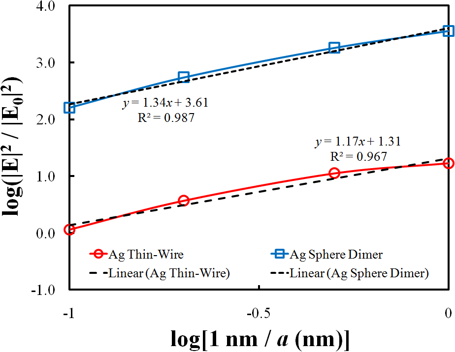
As a first example of the applicability of our analysis to real 3D structures, FEM was used to calculate the dependence at the center of a 3D Ag thin-wire antenna with nm and nm (both in and out of the plane of Fig. 1) at nm; Fig. 3.

It is found that is again approximately , which is nearly equal to the analogous 2D PEC thin-wire antenna results in Fig. 2. Further similarity comes from the behavior as decreases, where the dependence again becomes weaker, as can be inferred from the curvature of the actual data relative to the linear fit.
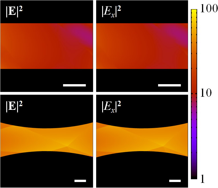
It is possible to verify the existence of a TEM waveguide mode by looking at profiles of E inside the gap, as for normal incident linearly-polarized light this mode has the same polarization. Figure 4 shows the fields inside the gap of the antenna discussed above for nm, and it can be seen that this is indeed the case, as .

(Note that and are both less than on the scale in Fig. 4.) In fact, it has recently been demonstrated experimentally that electromagnetic fields inside the gaps of nanostructures are linearly polarized, even in more complex ones than discussed here Schnell, et al. (2010).
As a further and final example of the applicability of our analysis to real 3D structures, enhancements as a function of gap size were calculated for a dimer of nm diameter Ag spheres at nm (a popular type of experimental system and common laser wavelength Wustholz et al. (2010)); Fig. 3. The dependence in this case is found to be characterized by , which is nearly equal to the modal result of , and slightly greater than the somewhat analogous thin-wire antenna result in Fig. 3. The stronger dependence is related to the fact that this structure is more efficient for capturing light Bohren and Huffman (1983), as indicated by as opposed to for the thin-wire antenna, for example. Field profiles inside the gap again indicate the presence of a TEM waveguide mode; Fig. 4. Looking closely at Fig. 3 reveals that there is a much less strong turnover to a weaker dependence for smaller than was seen for any of the other structures. Such behavior is understandable considering that is effectively zero in this case (there is only a single point of minimum approach), which can lead to being unbounded as [; see Eq. (10)]. It is quite remarkable that the simple analysis derived for a 2D PEC film with an isolated slit is so accurate when applied to full 3D structures of other geometries, and even in the presence of SPs.
Acknowledgements.
J.M.M. and G.C.S. were supported by a Grant from the U. S. Department of Energy, Office of Science, Office of Basic Energy Sciences, under Award No. DE-SC0004752. Use of the Center for Nanoscale Materials was supported by the U. S. Department of Energy, Office of Science, Office of Basic Energy Sciences, under Contract No. DE-AC02-06CH11357.References
- Moskovits (1985) M. Moskovits, Rev. Mod. Phys. 57, 783 (1985).
- García-Vidal and Pendry (1996) F. J. García-Vidal and J. B. Pendry, Phys. Rev. Lett. 77, 1163 (1996).
- Schuck et al. (2005) P. J. Schuck, D. P. Fromm, A. Sundaramurthy, G. S. Kino, and W. E. Moerner, Phys. Rev. Lett. 94, 017402 (2005).
- Mühlschlegel et al. (2005) P. Mühlschlegel, H.-J. Eisler, O. J. F. Martin, B. Hecht, and D. W. Pohl, Science 308, 1607 (2005).
- Kang et al. (2009) J. H. Kang, D. S. Kim, and Q.-H. Park, Phys. Rev. Lett. 102, 093906 (2009).
- Wustholz et al. (2010) K. L. Wustholz, A.-I. Henry, J. M. McMahon, R. G. Freeman, N. Valley, M. E. Piotti, M. J. Natan, G. C. Schatz, and R. P. Van Duyne, J. Am. Chem. Soc. 132, 10903 (2010).
- Hao and Schatz (2004) E. Hao and G. C. Schatz, J. Chem. Phys. 120, 357 (2004).
- Aizpurua et al. (2005) J. Aizpurua, G. W. Bryant, L. J. Richter, F. J. García de Abajo, B. K. Kelley, and T. Mallouk, Phys. Rev. B 71, 235420 (2005).
- Romero et al. (2006) I. Romero, J. Aizpurua, G. W. Bryant, and F. J. García de Abajo, Opt. Express 14, 9988 (2006).
- Kottmann and Martin (2001) J. P. Kottmann and O. J. F. Martin, Opt. Express 8, 655 (2001).
- Jin (2002) J. Jin, The Finite Element Method in Electromagnetics (John Wiley & Sons, Inc.: New York, 2002), ed.
- Bravo-Abad et al. (2004) J. Bravo-Abad, L. Martín-Moreno, and F. J. García-Vidal, Phys. Rev. E 69, 026601 (2004).
- Kraus and Marhefka (2001) J. D. Kraus and R. J. Marhefka, Antennas (McGraw-Hill Education: Singapore, 2001), ed.
- Pohl (2000) D. W. Pohl, in Near-Field Optics: Principles and Applications, edited by M. Ohtsu and X. Zhu (World Scientific: Singapore, 2000).
- McMahon et al. (2009) J. M. McMahon, S. K. Gray, and G. C. Schatz, Phys. Rev. Lett. 103, 097403 (2009).
- Jackson (1998) J. D. Jackson, Classical Electrodynamics (John Wiley & Sons, Inc.: New York, 1998), ed.
- Slater and Frank (1969) J. C. Slater and N. H. Frank, Electromagnetism (Dover Publications, Inc.: New York, 1969).
- Bohren and Huffman (1983) C. F. Bohren and D. R. Huffman, Absorption and Scattering of Light by Small Particles (John Wiley & Sons, Inc.: New York, 1983).
- Schnell, et al. (2010) M. Schnell, A. Garcia-Etxarri, J. Alkorta, J. Aizpurua, and R. Hillenbrand, Nano. Lett. 10, 3524-3528 (2010).