Conductivity of a graphene strip: width and gate-voltage dependencies
Abstract
We study the conductivity of a graphene strip taking into account electrostatically-induced charge accumulation on its edges. Using a local dependency of the conductivity on the carrier concentration we find that the electrostatic size effect in doped graphene strip of the width of 0.5 - 3 m can result in a significant (about 40%) enhancement of the effective conductivity in comparison to the infinitely wide samples. This effect should be taken into account both in the device simulation as well as for verification of scattering mechanisms in graphene.
pacs:
72.80.Vp, 73.23.-b, 73.50.DnDescription of the electron transport in wide graphene sheets is usually based on the Boltzmann approach under the assumption of a homogeneous distribution of the electron density, see Refs. 1-3 for a review. In the opposite limit of ultranarrow strips (nanoribbons) the transport is described within the Landauer-Buttiker approach. With increase of the width of the strip, , the quasiclassical size-dependent effect, when both in-plane and edge scattering mechanisms are essential, takes place. In a typical sample, this regime can be realized at m; here is the mean free path. Further increase of the width, when becomes comparable to the thickness of a dielectric layer, , results in an electrostatically-induced size-dependent modifications of longitudinal transport caused by a redistribution of the in-plane density near edges of the strip. Such the redistribution takes place in any capacitor under the applied gate voltage and is illustrated in Fig. 1 for different aspect ratios . 5 Recently, it has been demonstrated that a pronounced charge accumulation takes place at the edges of a graphene strip 6 . It is therefore important to investigate how this charge accumulation affects the conductivity of realistic graphene samples.
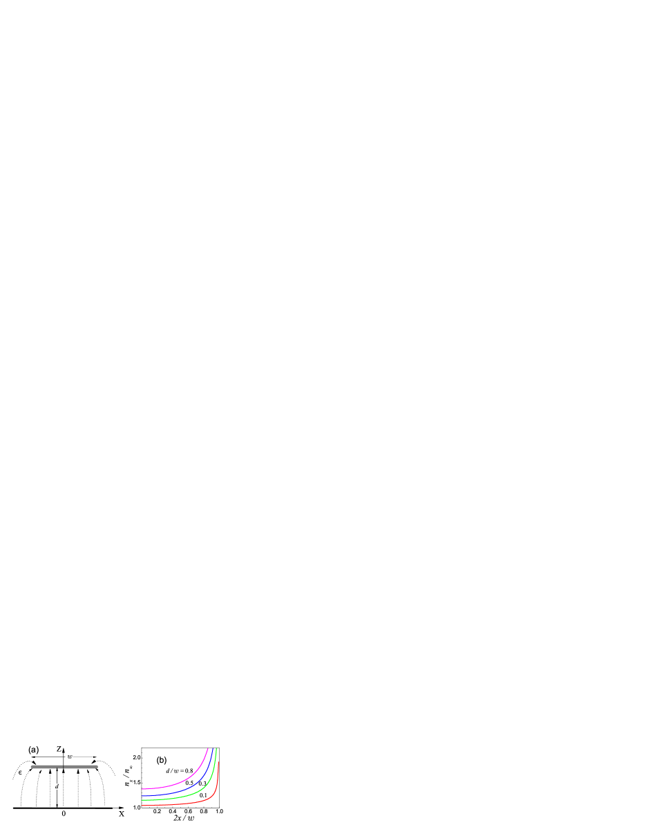
In this paper, we calculate the low-temperature conductivity of a graphene strip within the local approximation when the mean free path is less than the scale of the concentration inhomogeneity on the boundary (which is . For the sake of simplicity we restrict ourselves to the case of the uniform dielectric permittivity, , i.e. we consider a structure with cup layer (the effect should increase for the SiO2-graphene structure, see 6 ). A current of the density flows in the 0Y-direction, see Fig. 1a. Because of the redistribution of the in-plane density along 0X-direction near the edges as discussed above, the local conductivity and the electric field are dependent on the transverse coordinate such that . Since const due to the continuity equation , we obtain the average electric field
| (1) |
Introducing the relation between and through the effective conductivity, , we obtain
| (2) |
Below we calculate using the concentration distribution for a capacitor 5 (see Fig. 1b and Ref. 4b for details of calculations) and the local quasiclassical conductivity which depends on the density parametrically.
For the zero-temperature case, the local conductivity can be written through the -dependent Fermi momentum, , as follows (see 1 ; 2 ; 3 ; 7 ; 8 for details):
| (3) |
Here cm/s, 12.9 k, and is the momentum relaxation rate. In order to check a sensitivity of the size effect under consideration to scattering details, we consider here the momentum relaxation rates caused by: (I) Gaussian and short-range disorder potentials, 7 ; 8 with the total relaxation rate , and (II) Coulomb and short-range disorder potentials, 3 with the total rate . The Gaussian disorder is described by the potential with the Gaussian correlation function , where is the averaged energy and is the correlation length. Within the Born approximation, the correspondent relaxation rate reads where we have introduced the dimensionless function with the first-order Bessel function of an imaginary argument, and the characteristic velocity . The relaxation rate due to the short-range disorder potential within the Born approximation has a similar (if ) dependence , with an explicit expression for the characteristic velocity given in Refs. 6b and 7a. Note that in the present study we limit ourselves to the case of weak short-range scattering, as opposed to the case of strong resonant short-range scattering where has a different functional dependence and can not be described within the Born approximation [6b, 7b]. Since our aim is to demonstrate that the size-effect under consideration is generic for graphene strips and takes place for different scattering conditions, a comparative discussion of scattering mechanisms is beyond the scope of this work. The momentum relaxation rate due to scattering by charged Coulomb impurities of concentration is given by 3 , where the screening effect is omitted (screening reduces but does not change the relation ).
Using these relaxation rates in Eq. (3) we obtain for the local conductivity for the cases (I) and (II),
| (4) |
where . Further, substituting (4) into Eq. (2) and performing numerical integration we obtain the effective conductivity versus and for the cases (I) and (II).
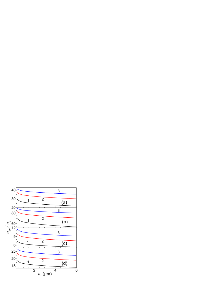
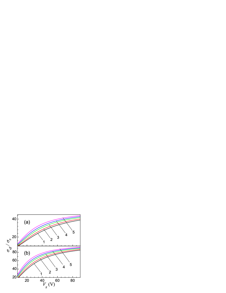
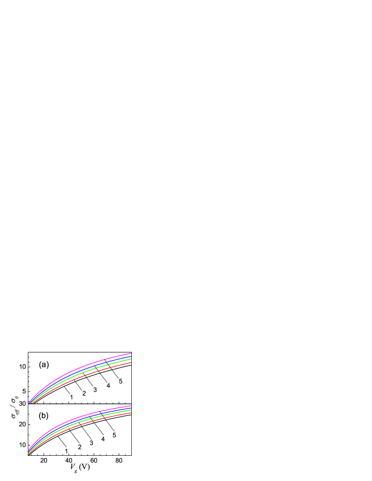
Figure 2 shows the gate voltage dependence for for the case (I) for different , , and relative widths, . The ratio =0.3 is used and these parameters are correspondent to a sample with maximal resistance per square 2 k). In Fig. 3 the same dependencies are presented for the case (II) for the values of and corresponding to the maximal resistance 4 k. Since the local conductivity (4) increases with the carrier concentration (at 100 V the saturation due to the short-range scattering takes place), increases with in agreement with the concentration dependency shown in Fig. 1b. A decrease of with increase of the width of the strip, , is shown in Fig. 4 for the cases presented in Figs. 2 and 3 for different . For the effective conductivity can exceed the corresponding conductivity for the infinite sample up to 50%. For a more narrow strip, shows even stronger increase; however it is not apparent that the local approximation is valid in realistic systems when .
Next, we briefly discuss the reported transport measurements in graphene 1 ; 2 ; 3 ; 9 ; 10 ; 11 ; 12 ; 13 in relation to our results concerning the electrostatically-induced size-dependent modifications of the longitudinal conductivity. Only in a few cases, 11 the condition was satisfied and the size effect under consideration was not essential. In some papers, 12 a situation is not clear due to the effect of side gate or/and additional contacts along a conducting canal. In other measurements, e.g. in 13 , the dependency is expected to be affected due to the electrostatic size effect. However, a verification of a size effect through dependencies is uncertain because these dependencies are similar for the cases (I) and (II) above. In addition, a microscopic mechanism of scattering in graphene remains under debate. 3 ; 14 Direct measurements of the size-dependent conductivity can be performed using a set of samples of different widths made from the same flake (to avoid contact effect these samples should be long enough) or with a multi-contacted sample formed by fragments of different widths, similar to those used in Ref. 10b. Note also a possibility for direct STM measurements of a lateral charge distribution. In addition, the quasiclassical magnetotransport should be modified if 0.1.
Let us finally list the assumptions used in our calculations. The local approach is valid when the characteristic scale of a charge redistribution () exceeds the mean free path (, is the relaxation time and m for a typical case; for the non-local regime, at , a size dependency should be modified, but not suppressed). Here we consider a simple capacitor geometry with homogeneous ; more complicate calculations are necessary to account for discontinuity of on the dielectric/air interface. Finally, we limited ourselves to the standard regime of quasiclassical transport (the Boltzmann equation approach and no electron/hole puddles formation at low ) and we do not consider a temperature dependency of conductivity.
In summary, we have demonstrated that the electrostatic size effect in doped graphene strips of width 0.5 - 3 m results in a visible (about 40%) enhancement of the effective conductivity. This should be taken into account both for device simulation and for verification of scattering mechanisms in graphene.
F.T.V. acknowledges support from the Swedish Institute. I.V.Z. acknowledges support from the Swedish Research Council (VR).
References
- (1) A. H. Castro Neto, F. Guinea, N.M.R. Peres, K.S. Novoselov, and A.K. Geim, Rev. Mod. Phys. 81, 109 (2009).
- (2) D. S. L. Abergel, V. Apalkov, J. Berashevich, K. Ziegler, T. Chakraborty, Adv. Phys. 59, 261 (2010); E. R. Mucciolo and C. H. Lewenkopf, J. Phys.: Condens. Matter 22, 273201 (2010).
- (3) S. Adam, E.H. Hwang, E. Rossi, S. Das Sarma, Solid State Comm. 149, 1072 (2009); S. Das Sarma, S. Adam, W. H.Hwang, and E. Rossi, arXiv:1003.4731.
- (4) P. M. Morse and H. Feshbach, Methods of Theoretical Physics, Part II (McGraw-Hill, New York, 1963); H. Nishiyama and M. Nakamura, IEEE Trans. on Components, Hybrides, and Manufacting Technology, 13, 417 (1990).
- (5) P. G. Silvestrov and K. B. Efetov, Phys. Rev. B 77, 155436 (2008); A. A. Shylau, J. W. Klos and I. V. Zozoulenko, Phys. Rev. B 80, 205402 (2009)
- (6) N. M. R. Peres, J. M. B. Lopes dos Santos, and T. Stauber, Phys. Rev. B 76, 073412 (2007); T. Stauber, N. M. R. Peres, and F. Guinea. Phys. Rev. B 76, 205423 (2007).
- (7) F.T. Vasko and V. Ryzhii, Phys. Rev. B 76, 233404 (2007); J. W. Klos and I. V. Zozoulenko, Phys. Rev. B, in press (2010).
- (8) K. S. Novoselov, A. K. Geim, S. V. Morozov, D. Jiang, Y. Zhang, S. V. Dubonos, I. V. Grigorieva, and A. A. Firsov, Science 306, 666 (2004); A. K. Geim and K. S. Novoselov, Nat. Mater. 6, 183 (2007).
- (9) Y. Zhang, Y.-W. Tan, H. L. Stormer, and P. Kim, Nature 438, 201 (2005); Y.-W. Tan, Y. Zhang, H. L. Stormer, and P. Kim, Eur. Phys. J. Spec. Top. 148, 15 (2007).
- (10) Y.-W. Tan, Y. Zhang, K. Bolotin, Y. Zhao, S. Adam, E. H. Hwang, S. Das Sarma, H. L. Stormer, and P. Kim, Phys. Rev. Lett. 99, 246803 (2007); C. Jang, S. Adam, J.-H. Chen, E. D. Williams, S. Das Sarma, and M. S. Fuhrer, Phys. Rev. Lett. 101, 146805 (2008).
- (11) X. Hong, K. Zou, and J. Zhu, Phys. Rev. B 80, 241415 (2009); W. Zhu, V. Perebeinos, M. Freitag, Ph. Avouris, Phys. Rev. B 80, 235402 (2009).
- (12) K. S. Novoselov, A. K. Geim, S. V. Morozov, D. Jiang, M. I. Katsnelson, I. V. Grigorieva, S. V. Dubonos, and A. A. Firsov, Nature 438, 197 (2005).
- (13) L. A. Ponomarenko, R. Yang, T. M. Mohiuddin, M. I. Katsnelson, K. S. Novoselov, S. V. Morozov, A. A. Zhukov, F. Schedin, E. W. Hill, and A. K. Geim, Phys. Rev. Lett. 102, 206603 (2009).