Strong and Tunable Spin–Orbit Coupling of One-Dimensional Holes in Ge/Si Core/Shell Nanowires
Abstract
We investigate the low-temperature magneto-transport properties of individual Ge/Si core/shell nanowires. Negative magneto-conductance was observed, which is a signature of one-dimensional weak antilocalization of holes in the presence of strong spin–orbit coupling. The temperature and back gate dependences of phase coherence length, spin–orbit relaxation time, and background conductance were studied. Specifically, we show the spin–orbit coupling strength can be modulated by more than five folds with an external electric field. These results suggest the Ge/Si nanowire system possesses strong and tunable spin–orbit interactions and may serve as a candidate for spintronics applications.
Semiconductor nanowires exhibit novel electrical, optical, and mechanical properties and offer substantial potential as building blocks of nanodevices owing to their one-dimensional structure 1, 2, 3. Besides being a good candidate for high performance electronic devices, nanowires may also be used in the field of spintronics, which involves exploration of the extra degrees of freedom provided by electron spin, in addition to those due to electron charge 4, 5. In particular, Ge/Si core/shell nanowires represent a unique one-dimensional system for exploring quantum coherence phenomenon at the nanoscale because of their high hole mobility and strong quantum confinement effects 6, 7, 8, 9. In addition, as compared with III–V materials (for example, InAs) where hyperfine coupling limits the electron spin coherence, the prospect of long coherence times in group IV materials due to the predominance of spin-zero nuclei has stimulated several proposals and significant experimental effort for spin-based quantum information applications 5, 10, 11. One key to realizing such promise is the utilization of spin–orbit interaction which can be controlled by tuning the applied gate voltages. However there are few investigations of spin–orbit interactions and corresponding relaxation times in group IV semiconducting nanowires. Here, we report on low-temperature magneto-conductance measurements of individual gated Ge/Si core/shell nanowires in transverse magnetic field. The observed negative magneto-conductance data are consistent with the one-dimensional weak antilocalization effect of holes in the presence of strong spin–orbit interactions 11, 12, 13, 14, 15. We extract the phase coherence length/time, the spin–orbit coherence length/time, and the spin–orbit coupling constant, and verify both the hole phase coherence and the spin–orbit coupling can be tuned in our system as a function of gate voltage. The gate-tunable spin–orbit coupling strength suggests the Ge/Si core/shell nanowire is a candidate platform for designing future spintronics applications 5.
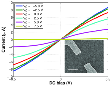
The undoped Ge/Si core/shell nanowires studied here, which have an average germanium core of nm and silicon shell of nm, were grown using a two-step chemical vapor deposition process reported earlier 6. The nanowires were suspended by ultrasound sonication in isopropyl alcohol, then deposited onto nm thick oxide on a degenerately doped Si substrate. The Si substrate was also used as a bottom gate electrode. After nanowire transfer, source and drain contacts were defined by electron-beam lithography. To make good contacts between metal leads and the Ge core of the nanowires, the samples were treated in buffered hydrofluoric acid for s to remove any native oxide on top of the Si shell before electron-beam evaporation of source/drain electrodes (palladium, nm thick). A total of three devices from the same batch of nanowires were studied, and all have produced remarkably remarkably similar results. For consistency, we present here the data (including the mobility and density value) from only one device. The scanning electron microscope (SEM) image of a similar device is shown in the inset of Fig. 1(a). In Fig. 1(a), the current is plotted against bias voltage at several different back gate voltages at the temperature of mK. The low-temperature linearities of these characteristics, especially at zero bias, verify good Ohmic contacts between metal leads and the nanowire were achieved. We also observed signs of possible multiple subbands transport through the nanowire at different temperatures (see Supporting Information Fig. 5) similar to our earlier studies 6. Using the transport data and taking into account of the gate capacitance , which is given by the cylinder-on-plane model 16, the hole mobilities of the device can be calculated as followsing 6, 17:
| (1) |
Here, was obtained from the linear region of the data (see Supporting Information Fig. 5 and Fig. 6), m is the length of the nanowire between two contacts of the device, and is the source-drain voltage at which the data were taken. A mobility of cm2V-1s-1 at room temperature and of cm2V-1s -1 at liquid Helium temperature were determined. These values are consistent with previous results 7 in Ge/Si core/shell nanowires.
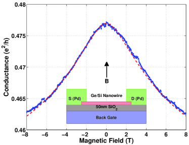
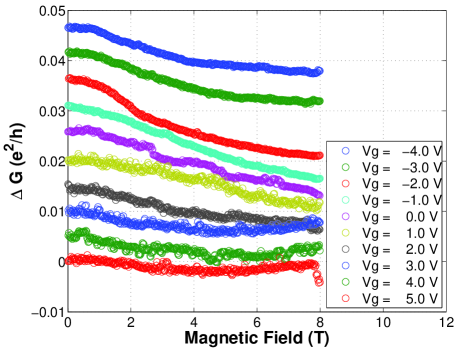
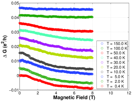
Magneto-conductance measurements were carried out with the external magnetic field applied perpendicular to the axis of the nanowire as well as the substrate (inset of Fig. 1(b)). The two-terminal magneto-conductance of the nanowire was measured using quasi-dc lock-in technique with a bias voltage of mV at Hz in a Quantum Design Physical Properties Measurement System cryostat. Data from one of the magneto-conductance measurements were plotted in Fig. 1(b), in which a clear magneto-conductance peak (blue dotted line) at the center of magnetic field was observed. Magneto-conductance data at different gate voltages and different temperatures are plotted in Fig. 7 and Fig. 8 in the Supporting Information. It is well known that the quantum interference of the electron wave functions reduces (increases) backscattering of the electrons from impurities and therefore, increases (decreases) the conductance from its Drude value leading to weak antilocalization (localization) effects in systems with (without) strong spin–orbit interactions 12. Applying a magnetic filed perpendicular to the sample destroys these interference effects and restores the conductance to its Drude value. The present observation is consistent with the suppression of the weak antilocalization by the external magnetic field. The presence of weak antilocalization in our experiment indicates strong spin–orbit coupling in this system 11. It is important to note that unlike previous reports on arrays of quantum dots 18, nanowires 14 or two dimensional system 19, the interpretation of our data is based on weak-antilocalization effect of hole gas in an individual nanowire without any average 15.
In an one-dimensional system, at a magnetic field , the weak antilocalization correction including the spin–orbit interaction effect to the conductance is given by 12, 13, 14, 15:
| (2) | |||||
Here, is the electric charge of electron, is the Planck constant, is phase coherence length, is the spin–orbit coherence length, is the elastic mean-free path. is the diffusion coefficient 13. is the background conductance (Drude value) without the localization or antilocalization correction. is the relaxation time due to external magnetic field, for which we use the expression in the case of specular boundary scattering in one-dimensional channel 13. is the diameter of the conductance channel (nanowire diameter). is the effective mass of hole in Ge. The hole density and mobility can be estimated from the transport data. is the Fermi wavelength and is the Fermi wave velocity. The estimated value is around nm, and the estimated value is around nm (Both and depend on the gate voltage and the temperature). Since our system is in the regime , Eq. 2 is suitable for our case. In addition, since this fitting equation is only valid for , we restricted our fitting to the data where the magnetic field is smaller than T. Overall there are three parameters , and in Eq. 2 that are used to fit our experimental data. One of the fitting curves is indicated by the red dashed line in Fig. 1(b) and the fitted at mK are shown in Fig. 2(a) for different back gate voltages . There is an apparent overall decrease of in the range between V. This can be explained as the holes lose phase coherence as the device becoming more insulated 20. This change demonstrates that the carrier coherence properties can be controlled by tuning the gate voltage over a wide range 15, 21. From the fitting data, we also obtained the phase relaxation time , which is consistent with the values obtained from weak localization of holes in p-SiGe quantum wells 22, 23. The extracted phase coherence times at the same gate voltage follows a power law dependence of temperature , as shown in Fig. 2(b), which is observed previously in several other one-dimensional systems 24, 25, 26, 27, 28. The dependence of indicates that the scattering mechanism is dominated by the Nyquist process, in which the inelastic hole–hole collision happens with small energy exchange 24. At low temperatures, is found to saturate, which is a signature of either the heating the carriers by current 29 or external microwave noise 30.
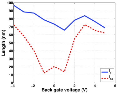
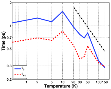
Fig. 2(a) also shows the extracted spin–orbit coherence length as a function of the gate voltages. The extracted values of are in the range nm at mK. The spin–orbit relaxation time shown in Fig. 2(b) is deduced from . It is interesting to note that unlike earlier studies on electron gas systems which show that is independent of temperature 15, 31, in our case we found decreases by about two folds as the temperature is increased to K from K, indicating that hole–hole scattering and phonon scattering accelerate the spin relaxation at high temperatures 32.
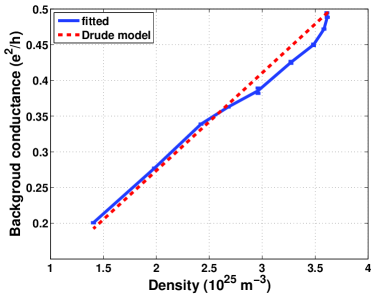
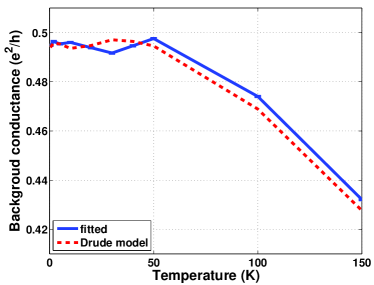
To further confirm the validity of the fitting method, the background conductance obtained from fitting using Eq. 2 was compared with that estimated using the Drude classical conductance model for the one-dimensional nanowire:
| (3) |
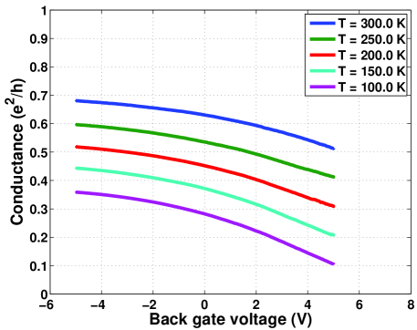
where and are density and mobility of the nanowire estimated from transport data. We plotted the fitted background conductance as well as the values estimated from the Drude model in Fig. 3 for different densities (Fig. 3(a)) and different temperatures (Fig. 3(b)). It is found the extracted values are in good agreement with the estimated Drude conductance, which implies the weak antilocalization dominates the transport and the model is well described by Eq. (2). Fig. 3(a) shows that the conductance decreases monotonically with the decrease of the hole density, as expected. We also found in Fig. 3(b) that the background conductance keeps increasing when the temperature decreases before K, which indicates the suppression of hole-phonon interaction at lower temperatures. In addition, saturates below K, which is likely due to the effect of residual impurity scattering inside the nanowire 21.
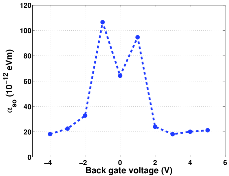
We now discuss spin–orbit coupling in this system. Since both bulk Si and Ge have an inversion center 33, in our analysis we do not include the Dresselhaus effect, which is induced by bulk inversion asymmetry 34. The Elliott-Yafet effect, which is caused by the lattice vibrations and impurity scattering 35, was also neglected due to the high hole mobility and the observed effect that the spin–orbit coherence length is a strong function of (Fig. 2(a)) but the mobility is insensitive to . To obtain the spin–orbit coupling strength , we only include the Rashba effect, which originates from the structural inversion asymmetry of the device geometry and can me modulated by external potential 36, 19, 37:
| (4) |
where is the Fermi wave number, and is the transport relaxation time. In this way, the spin–orbit coupling strength can be deduced from the weak antilocalization measurements, as shown in Fig. 4. Significantly, we note that the spin–orbit coupling strength decreases by more than five folds as the absolute value of the back gate voltage increases. The gate tunable spin–orbit coupling in Ge/Si core/shell nanowires in turn suggests the Ge/Si nanowire system is a suitable candidate in applications of spintronics device 38. In addition, a nonmonotonic back gate voltage dependence was observed for , (Fig. 2(a)) and (Fig. 4) around V 21. The nonmonotonic behavior might be caused by intersubband scattering between multiple subbands involved into the magneto-transport 6, 28, or how the original asymmetry of the confinement well profile is canceled by external electric field at small field 37, which need further investigation.
In conclusion, we observed weak antilocalization of one-dimensional holes in an individual Ge/Si core/shell nanowires with strong spin–orbit coupling. The phase coherence length, the spin–orbit coherence length as well as the spin–orbit coupling strength and background conductance were extracted by fitting the experimental data at different temperatures and gate voltages. Both the phase coherence length and the spin–orbit coupling strength were found to be adjustable by an external electric field. Our results illustrate the potential of chemically synthesized Ge/Si core/shell nanowires in future spintronics applications, and using this system as a platform for studying coherent spintronics phenomena of holes in low-dimensions.
Acknowledgment.
This work was supported by the National Science Foundation (ECS-0601478), the National Basic Research Program of China (Grants No. 2009CB929600, No. 2006CB921900), and the National Natural Science Foundation of China (Grants No. 10804104, No. 10874163, No. 10934006).
Supporting Information Available.
Conductance and magneto-conductance at different temperatures and gate biases and effects of Pd electrodes on the magneto-conductance effects. This material is available free of charge via the Internet at http://pubs.acs.org.
References and Notes
References
- 1 Lieber, C. M. MRS Bull. 2003, 28, 486.
- 2 Lu, W.; Lieber, C. M. J. Phys. D 2006, 39, R387.
- 3 Thelander, C.; Agarwal, P.; Brongersma, S.; Eymery, J.; Feiner, L.; Forchel, A.; Scheffler, M.; Riess, W.; Ohlsson, B.; Gösele, U.; Samuelson, L. Mater. Today 2006, 9, 28.
- 4 Wolf, S. A.; Awschalom, D. D.; Buhrman, R. A.; Daughton, J. M.; von Molnar, S.; Roukes, M. L.; Chtchelkanova, A. Y.; Treger, D. M, Science 2001, 294, 1488.
- 5 Awschalom, D.; Loss, D.; Samarth, N., Semiconductor Spintronics and Quantum Computation Springer-Verlag: Berlin, 2002.
- 6 Lu, W.; Xiang, J.; Timko, B. P.; Wu, Y.; Lieber, C. M. Proc. Natl Acad. Sci. U. S. A. 2005, 102, 10046.
- 7 Xiang, J.; Lu, W.; Hu, Y.; Wu, Y.; Yan, H.; Lieber, C. M. Nature 2006, 441, 489.
- 8 Xiang, J.; Vidan, A.; Tinkham, M.; Westervelt, R. M.; Lieber, C. M. Nature Nanotechnology, 2006, 1, 208.
- 9 Liang, G.; Xiang, J.; Kharche, N.; Klimeck, G.; Lieber, C. M.; Lundstrom, M. Nano Lett. 2007, 7, 642.
- 10 Hu, Y.; Churchill, H. O. H.; Reilly, D. J.; Xiang, J.; Lieber, C. M.; Marcus, C. M. Nature Nanotechnology 2007, 2, 622.
- 11 Roddaro, S.; Fuhrer, A.; Brusheim, P.; Fasth, C.; Xu, H. Q.; Samuelson, L.; Xiang, J.; Lieber, C. M. Phys. Rev. Lett. 2008, 101, 186802.
- 12 Hikami, S.; Larkin, A. I.; Nagaoka, Y. Prog. Theor. Phys. 1980, 63, 707.
- 13 Beenakker C. W.; Houten H. Phys. Rev. B 1988, 38, 3232.
- 14 Kurdak Ç.; Chang A. M.; Chin A.; Chang T. Y. Phys. Rev. B 1992, 46, 6846.
- 15 Hansen A. E.; Björk M. T.; Fasth C.; Thelander C.; Samuelson L. Phys. Rev. B 2005, 71, 205328.
- 16 Ramo, S.; Whinnery, J. R.; Duzer, T. V. Fields and Waves in Communication Electronics Wiley: New York, 1994.
- 17 Wang, D.; Wang Q.; Javey, A.; Tu, R.; Dai, H.; Kim, H. ; Krishnamohan, T.; McIntyre, P.; Saraswat. K. Appl. Phys. Lett. 2003, 83, 2432.
- 18 Faniel, S.; Hackens, B.; Vlad, A.; Moldovan, L.; Gustin, C.; Habib, B.; Melinte, S.; Shayegan, M.; Bayor, V. Phys. Rev. B 2007, 75, 193310.
- 19 Koga, T.; Nitta, J.; Akazaki, T.; Takayanagi, H. Phys. Rev. Lett. 2002, 89, 046801.
- 20 Nakamura, H.; Kimura, T. Phys. Rev. B 2009, 80, 121308(R).
- 21 Dhara, S.; Solanki, H. S.; Singh, V.; Narayanan, A.; Chaudhari, P.; Gokhale, M.; Bhattacharya, A.; Deshmukh, M. M. Phys. Rev. B 2009, 79, 121311.
- 22 Senz V.; Heinzel T.; Ihn Y.; Ennslin K.; Dehlinger G.; Grutzmacher D.; Gennser U. Phys. Rev. B 2000, 61, R5082.
- 23 Coleridge P. T.; Sachrajda A. S.; Zawadzki P. Phys. Rev. B 2002, 65, 125328.
- 24 Altshuler, B. L.; Aronov, A. G.; Khmelnitzky, D. E. J. Phys. C: Solid State Phys. 1982, 15, 7367.
- 25 Lin, J. J.; Giordano, N. Phys. Rev. B 1987, 35, 545.
- 26 Pierre, F.; Gougam, A. B.; Anthore, A.; Pothier, H.; Esteve, D.; Birge, N. O. Phys. Rev. B 2003, 68, 085413.
- 27 Chiquito, A. J.; Lanfredi, A. J. C.; de Oliveira, R. F. M.; Pozzi, L. P.; Leite, E. R. Nano Lett. 2007, 7, 1439.
- 28 Liang, D.; Sakr M. R.; Gao X. P. A. Nano Lett. 2009, 9, 1709.
- 29 Rueß, F. J.; Weber, B.; Goh, K. E. J.; Klochan, O.; Hamilton, A. R.; Simmons, M. Y. Phys. Rev. B 2007, 76, 085403.
- 30 Khavin, Y. B.; Gershenson, M. E.; Bogdanov, A. L. Phys. Rev. Lett. 1998, 81, 1066.
- 31 Guzenko, V. A.; Schäpers, T.; Hardtdegen, H. Phys. Rev. B 2007, 76, 165301.
- 32 Kallaher, R. L.; Heremans, J. J.; Goel, N.; Chung, S. J.; Santos, M. B. Phys. Rev. B 2010, 81, 035335.
- 33 Golub, L. E.; Ivchenko, E. L. Phys. Rev. B 2004, 69, 115333.
- 34 Dresselhaus, G. Phys. Rev. 1955, 100, 580.
- 35 Elliott, R. J. Phys. Rev. 1954, 96, 266.
- 36 Bychkov, Y. A.; Rashba, E. I. J. Phys. C 1984, 17, 6039.
- 37 Tahan, C.; Joynt, R. Phys. Rev. B 2005, 71, 075315.
- 38 Datta, S.; Das, B. Appl. Phys. Lett. 1990, 56, 665.
Supporting Information
Discussion on the possible influence of Pd contacts on the observed magnetoresistance effects.
We believe the observed magnetoresistance effects are intrinsic to the Ge/Si nanowire system due to the following reasons:
From the data in Phys. Rev. B 39, 915 (1989) and Phys. Rev. B 39, 3015 (1989), we resistance of the Pd leads was estimated to be less than k ( m nm nm), which is much smaller than the resistance of the nanowire ( k). In addition, the magnetoconductance effect in Pd films has been found to be only around based on the data in the references listed above. This effect is too small to explain the observed magnetoconductance of around observed in our system.
Furthermore, the magnetoconductance effects induced by the Pd contacts will be relevant when the magnetic length nm (thickness of the Pd electrodes), i.e. for magnetic field T. However, the magnetoconductance peak observed here covers several Tesla.
Finally, Aluminum contacted Ge/Si core/shell nanowire devices have also been tested and similar magnetoconductance effects were observed which are consistent with the results in this manuscript.