Optical Measurement of the Phase-Breaking Length in Graphene
Abstract
In mesoscopic physics, interference effects play a central role on the transport properties of conduction electrons, giving rise to exotic phenomena such as weak localization, Aharonov-Bohm effect, and universal conduction fluctuations. Mesoscopic objects have a size on the order of the phase-breaking length , the length conduction electrons travel while keeping phase coherence. In this letter, we use vibrational spectroscopy in combination with a novel optical defocusing method to measure of photo-excited electrons in graphene which undergo inelastic scattering by optical phonons. We extract from the spatial confinement of the defect-induced Raman D band near the edges of graphene. Temperature dependent measurements in the range of 1.55 K to 300 K yield , in agreement with previous magneto-transport measurements.
pacs:
78.67.Wj,72.80.Vp,78.67.-n,42.62.FiOver the past decades, silicon based materials spurred the development of ever smaller and faster transistor devices and the production of ever larger information storage. However, as the material dimensions become comparable to the length scale of electronic wavefunctions it is necessary to explore alternative materials with enhanced performance. Low-dimensional carbon materials, such as carbon nanotubes and graphene, form a particularly promising alternative to silicon based materials Avouris et al. (2007); Castro-Neto (2010).
Monolayer graphene exhibits unique electronic transport properties, such as high electron mobility at room temperature ( 104 cm2/Vs) and tunable carrier densities as high as 1013 cm-2 Geim and Novoselov (2007). These properties have led to extensive research and motivated the development of proof-of-concept devices, such as single electron transistors (SETs), field-effect transistors (FETs), and even graphene-based memory ensslin2008 ; Meric et al. (2008); Li et al. (2008a). Although single-crystal graphene is metallic (unable to confine electrons electrostatically), it can become semiconducting when produced in a narrow ( 10 nm) ribbon-like geometry, a manifestation
of electronic quantum confinement Avouris et al. (2007).
Conduction electrons confined to nanometer length scales cease to show a purely diffusing behavior as predicted by the Boltzmann transport theory. In this regime, the dephasing length of conduction electrons becomes larger than the device itself, and interference effects give rise to weak localization, Aharonov-Bohm effect, and universal conduction fluctuations Morozov et al. (2006); Wu et al. (2007); Tikhonenko et al. (2009); Lundeberg and Folk (2009).
These interference effects extend over the length , the electron phase-breaking length Taylor and Heinonen (2002); Beenakker and van Houten (1991). In this letter, we use Raman scattering to experimentally determine the phase-breaking length of photo-excited electrons near the edges of graphene, where electrons undergo inelastic scattering with optical phonons. The measurements were performed using a novel optical defocusing method, which makes it possible to measure the localization of the disorder-induced Raman D band Tuinstra and Koenig (1969) with a resolution of a few nanometers.
The relationship between the spatial confinement of the D band and the phase-breaking length has been debated recently Cançado et al. ; Casiraghi et al. (2009). In one interpretation, D band localization is predicted to depend on the virtual electron-hole lifetime and on the electron-phonon scattering rate Casiraghi et al. (2009). According to this interpretation, there is no direct relationship between D band localization and . In contrast, another interpretation predicts that D band localization is a direct consequence of the phase-breaking length and that can be measured by determining the spatial confinement of the D band Cançado et al. . To resolve this controversy, we have performed temperature-dependent measurements of D band scattering near the edges of graphene. As the temperature is decreased from 300 K to 1.55 K, the phonon population decreases and increases Beenakker and van Houten (1991); Morozov et al. (2006); Wu et al. (2007); Tikhonenko et al. (2009). Our measurements reveal that varies as , in agreement with magneto-transport measurements Morozov et al. (2006).
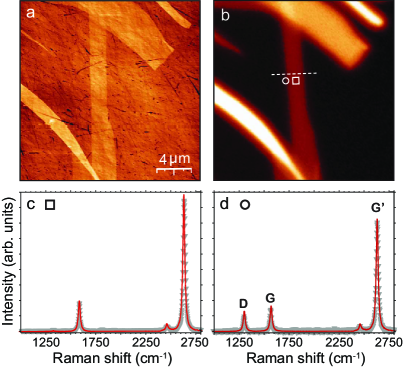
Figure 1(a) shows a topographic image recorded by atomic force microscopy (AFM) of a set of graphene pieces deposited on a fused silica surface. A corresponding confocal Raman image of the same region is depicted in Figure 1(b). The contrast (color scale) in the Raman image renders the intensity of the bond-stretching G band. The G band is a first-order scattering process that originates from the double-degenerate vibrational mode (E2g) that occurs at the crossing of the longitudinal optical (LO) and transverse optical (TO) phonon branches at the point in the 1st Brillouin zone of graphene Tuinstra and Koenig (1969). Figures 1(c,d) show full Raman scattering spectra acquired at two different locations indicated by the white square and circle in Fig. 1(b). Spectrum (c) was acquired from the interior of the graphene piece (m from the edge), whereas spectrum (d) was recorded with the incident laser focus centered at the left edge. Spectrum (c) shows two major Raman features: the G band occurring at 1580 cm-1, and the G band centered at 2700 cm-1. The G band originates from two-phonon Raman processes involving TO phonons Ferrari and Robertson (2001) whose wavevectors extend next to the corner of the 1st Brillouin zone ( and points). The single-Lorentzian shape of the G′ band indicates that the measured sample region is indeed a single-layer graphene piece Ferrari et al. (2006); Cançado et al. (2008).
Both G and G bands are also detected in the Raman spectrum of Figure 1(d) (obtained from the edge). In addition to the peaks identified in the previous spectrum, we now also observe the defect-induced D band centered at 1350 cm-1 Tuinstra and Koenig (1969). Due to momentum conservation, the TO phonons giving rise to this band only become Raman active if the electrons or holes involved in the scattering process undergo elastic scattering by a lattice defect, which in this case is provided by the graphene edge Cançado et al. (2004, ); Casiraghi et al. (2009). Therefore, the closer the position of a photo-excited electron to the graphene edge, the higher is its probability to be involved in D band scattering. Notice that, although the G band is the overtone of the D band, it does not require the presence of defects to become Raman active, since momentum conservation is guaranteed in two-phonon Raman processes. The Raman spectra shown in Figures 1(c,d) were recorded with the polarization vector of the excitation laser beam oriented parallel to the graphene edge, since polarizations perpendicular to the edge do not generate D band scattering Cançado et al. (2004); Casiraghi et al. (2009).
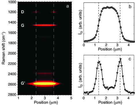
In order to analyze the spatial dependence of the D, G, and G intensities we have recorded Raman scattering spectra for different positions of the laser focus relative to the graphene edge. The incident beam was moved in steps of 100 nm along a 5 m long line perpendicular to the edges of a narrow graphene piece [dashed line in Figure 1(b)]. Figure 2(a) shows a hyperspectral Raman map recorded along the scan line. The horizontal axis refer to the spatial position of the incident laser (in m units) and the vertical axis renders the Raman shift. As the graphene piece is stepped through the laser focus, the intensities of the G and G bands gradually transit from a minimum value (dark counts) to a maximum value. On the other hand, the D band intensity achieves a maximum value when the graphene edge is in the laser focus. Figures 2(b) and 2(c) show the intensity profile of the G and D bands, respectively, obtained from the hyperspectral data shown in panel (a).
Because the intensity profile of the incident laser beam corresponds to a finite point-spread function (PSF), the intensity profiles shown in Figs. 2(a-c) originate from the spatial convolution of the Raman susceptibilities with the strength of the incident electric field. Initial attempts to determine the spatial confinement of the D band have been made by making use of prior information about the PSF of a strongly focused beam Cançado et al. . This prior knowledge was used to deconvolve the D band confinement from the recorded scan profile across a graphene edge. However, this method was only able to provide an upper limit of about 20 nm Cançado et al. and is not accurate enough to quantitatively determine the D band confinement. To overcome previous limitations we here introduce a defocusing technique to extract from the ratio of G and D band intensities.
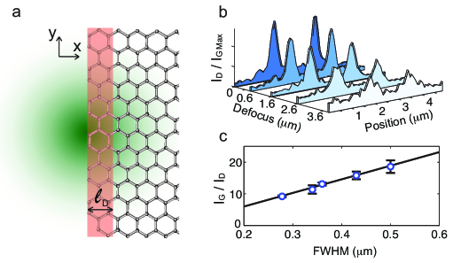
When the laser focus is centered at the edge of the graphene piece, the G band intensity () is proportional to the area of the laser focus, whereas the D band intensity is zero in absence of defects. D band scattering can be observed once the laser focus is placed near a graphene edge, which serves as a one-dimensional model defect. As depicted in Figure 3(a), the D band intensity () is proportional to the area defined by the spatial D band confinement (measured from the edge) and the length of the graphene edge exposed to the incident laser beam. Hence, the intensity ratio turns out to be proportional to the full-width-at-half-maximum (FWHM) of the point-spread function. For a Gaussian focus of width , this result can be formally derived as
| (1) |
| (2) |
where the lateral position of the edge is fixed at = 0 (see Fig. 3a for reference). and are the Raman susceptibilities of the G and D bands, respectively. Notice that we have considered in Eq. (2). The ratio obtained from Eqs. (1) and (2) for the focus centered at the edge gives
| (3) |
where we have used the relation , with being the FWHM. is the ratio between the strengths of the G and D bands in graphene, and has been empirically determined in Ref. Lucchese et al. (2010) to have a value of 0.24.
According to equation (3), the plot of the ratio versus gives a line whose slope is proportional to . Therefore, the width can be experimentally determined by performing several line scans with different amounts of defocus, which means different values. Since , as shown in Ref. Cançado et al. , the spatial profile of the D band is a good approximation to the line response function of the focus and can be used as a direct measurement of . The ratio for different amount of defocus is shown in Fig 3(b), where is the value taken from the center of the sample. Figure 3(c) shows the plot versus for the experimental data obtained using this technique at room temperature. The linear fit (solid line) gives 42 m-1 , which according to equation (3) leads to 3 nm. This is in excellent agreement with recent work by Lucchese et al. where the authors have measured a D band relaxation length of 3 nm, for point defects in ion bombarded graphene samples Lucchese et al. (2010).
Let us now discuss the physical origin of the D band confinement . A recent work Basko (2009) have explained that for any one-phonon Raman scattering process (such as D band scattering) the relaxation length is associated with the virtual electron-hole pair lifetime. The authors argued that since the energy uncertainty in such a process is determined by the phonon energy , the minimum value for the electron-hole pair lifetime obtained from the uncertainty principle is 1/. By using the relation , where is the group velocity of the photo-excited electrons, the authors have found 4 nm. This value is in agreement with the result obtained here, and also in Ref. Lucchese et al. (2010). However, this picture only gives an estimate for the minimum scattering length for the D band and does not explain the underlying physical mechanisms.
The phase-breaking length of a conduction electron is defined as the average distance traveled before undergoing inelastic scattering Taylor and Heinonen (2002); Beenakker and van Houten (1991). Since electrons involved in D band Raman scattering undergo a single inelastic scattering event with a lattice phonon, must correspond to the average distance traveled by such electrons during the time interval in which the D band scattering process takes place, that is = . By cooling the graphene sample we are able to reduce the phonon population and to decrease the probability of electrons to inelastically scatter by phonons. Thus, should increase as the temperature decreases. To verify this hypothesis, we have collected Raman scattering spectra for temperatures ranging from 1.55 K to 300 K. In Figure 4(a) we plot the ratio for different values of temperature along the scan line indicated in Figure 1(b). The experimental data show that the ratio increases as the temperature decreases (c.f. Figure 4a), indicating that the D band scattering length is indeed increasing. This result provides clear evidence for D band delocalization at low temperatures.
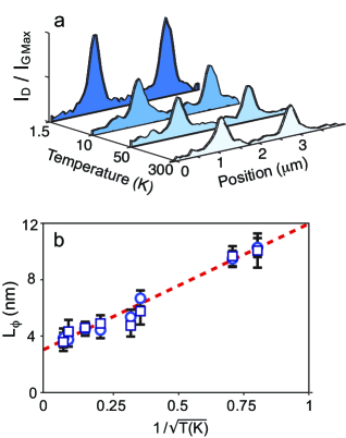
To quantify our experimental data and to relate the measurements to we have recorded the temperature dependence of by repeating the defocusing experiment in Figure 3(c) for different temperatures. The results are shown in Figure 4(b), which depicts as a function of inverse sample temperature for both edges. The solid line is a linear fit showing that . Since is known to be inversely proportional to Beenakker and van Houten (1991); Morozov et al. (2006)
our result provides strong evidence for the hypothesis that the spatial confinement of the D band indeed reflects the phase-breaking length.
The linear fit in Figure 3(b) yields , with a limiting value of = 3 nm for high temperatures ( 300 K). This result corroborates with our assumption that the value estimated for in Ref.Casiraghi et al. (2009) corresponds to the low limit for determined by the uncertainty principle. This limit is accurate for high phonon population regimes.
In summary, we have introduced a novel optical defocusing method for the measurement of the spatial confinement and temperature dependence of localized states, such as D band Raman scattering. Our measurements yield a D band confinement of nm at T=300 K and a temperature dependence of , which identifies as the phase-breaking length of photo-exited electrons or holes that undergo inelastic scattering by optical phonons. The technique developed here has clear advantages over standard transport measurements because contributions due to different scattering processes (electron-electron, electron-phonon, and electron-impurity) are not intermixed. The work demonstrates a strong connection between electronic and optical properties of graphene and shows that Raman spectroscopy provides an alternative tool for studying electric transport in mesoscopic structures.
Acknowledgements.
The authors would like to thank Christiane Höppener, Bradley Deutsch, Palash Bharadwaj, and Ado Jorio for valuable discussions and input. This work was supported by the Department of Energy (grant DE-FG02-05ER46207).References
- Avouris et al. (2007) P. Avouris, Z. Chen, and V. Perebeinos, Nature Nanotech. 2, 605 (2007).
- Castro-Neto (2010) A. H. Castro-Neto, Materials Today 13, 12 (2010).
- Geim and Novoselov (2007) A. K. Geim and K. S. Novoselov, Nature Phys. 6, 183 (2007).
- Novoselov et al. (2004) K. S. Novoselov et al., Science 306, 666 (2004).
- Berger et al. (2004) C. Berger et al., J. Phys. Chem. B 108, 19912 (2004).
- (6) C. Stampfer et al., Nano Lett. 8, 2378 (2008).
- Meric et al. (2008) I. Meric et al., Nature Nanotech. 3, 654 (2008).
- Li et al. (2008a) Y. Li, A. Sinitshii, and J. M. Tour, Nature Mat. 7, 966 (2008a).
- Levendorf et al. (2009) M. P. Levendorf, C. S. Ruiz-Vargas, S. Garg, and J. Park, Nano Lett. 9, 4479 (2009).
- Li et al. (2008b) X. Li, X. Wang, L. Zhang, S. Lee, and H. Dai, Science 319, 1229 (2008b).
- Dubois et al. (2009) S. M. M. Dubois, Z. Zanolli, X. Declerck, and J. C. Charlier., Eur. Phys. J. B 72, 1 (2009).
- Morozov et al. (2006) S. V. Morozov et al., Phys. Rev. Lett. 97, 016801 (2006).
- Wu et al. (2007) X. Wu, X. Li, Z. Song, C. Berger, and W. A. de Heer, Phys. Rev. Lett. 98, 136801 (2007).
- Tikhonenko et al. (2009) F. V. Tikhonenko, A. A. Kozikov, A. K. Savchenko, and R. V. Gorbachev, Phys. Rev. Lett. 103, 226801 (2009).
- Lundeberg and Folk (2009) M. B. Lundeberg and J. A. Folk, Nat. Phys. 5, 894 (2009).
- Taylor and Heinonen (2002) P. L. Taylor and O. Heinonen, A Quantum Approach to Condensed Matter Physics (Cambridge University Press, 2002).
- Beenakker and van Houten (1991) C. W. J. Beenakker and H. van Houten, Solid State Phys. 44, 1 (1991).
- Tuinstra and Koenig (1969) F. Tuinstra and J. L. Koenig, J. Chem. Phys. 53, 1126 (1969).
- (19) L. G. Cançado, R. Beams, and L. Novotny, Preprint at http://arxiv.org/abs/0802.3709 (2008).
- Casiraghi et al. (2009) C. Casiraghi et al., Nano Lett. 9, 1433 (2009).
- Ferrari and Robertson (2001) A. C. Ferrari and J. Robertson, Phys. Rev. B 64, 075414 (2001).
- Ferrari et al. (2006) A. C. Ferrari et al., Phys. Rev. Lett. 97, 187401 (2006).
- Cançado et al. (2008) L. G. Cançado, A. Reina, J. Kong, and M. S. Dresselhaus, Phys. Rev. B 77, 245408 (2008).
- Thomsen and Reich (2000) C. Thomsen and S. Reich, Phys. Rev. Lett. 85, 5214 (2000).
- Saito et al. (2001) R. Saito et al., Phys. Rev. Lett. 88, 027401 (2001).
- Cançado et al. (2004) L. G. Cançado et al., Phys. Rev. Lett. 93, 247401 (2004).
- Lucchese et al. (2010) M. M. Lucchese et al., Carbon 48, 1592 (2010).
- Basko (2009) D. M. Basko, Phys. Rev. B 79, 205428 (2009).
- Basko et al. (2009) D. M. Basko, S. Piscanec, and A. C. Ferrari, Phys. Rev. B 80, 165413 (2009).