Engineered arrays of NV color centers in diamond
based on implantation of CN- molecules through nanoapertures
Abstract
We report a versatile method to engineer arrays of nitrogen-vacancy (NV) color centers in diamond at the nanoscale. The defects were produced in parallel by ion implantation through 80 nm diameter apertures patterned using electron beam lithography in a PMMA layer deposited on a diamond surface. The implantation was performed with CN- molecules which increased the NV defect formation yield. This method could enable the realization of a solid-state coupled-spin array and could be used for positioning an optically active NV center on a photonic microstructure.
I Introduction
The nitrogen-vacancy (NV) color center in diamond, consisting of a substitutional nitrogen atom (N) associated to a vacancy (V) in an adjacent lattice site of the crystalline matrix, has found a wide range of applications in quantum information processing. It is a robust luminescent center which, once isolated at the individual level Gruber_Science_1997 , can be used to implement efficient single-photon quantum key distribution protocols Alleaume_NJP_2004 . Moreover, the association of a spin structure in the ground level having a long coherence time at room temperature with spin dependent optical transitions allows for quantum state preparation by optical pumping and single-spin quantum state readout Jelezko_PRL_2004 . However, development of most of the envisioned applications require to position the NV center with nanometer-scale accuracy. This spatial control could be the basic technology for building a scalable quantum simulator based on spins associated to an array of NV defects with magnetic dipolar coupling Neumann_NatPhys_2010 . The control of the position of a NV defect could also help to enhance the photon out-coupling by channeling its luminescence toward a photonic structure, like a dielectric nanowire Babinec_NatureNano_2009 or a metallic antenna Greffet_PRL_2009 .
A practical solution can consist in addressing NV centers in diamond nanocrystals Treussart_PhysB2006 . By manipulating the nanoparticle with a tip-based system Ampen-Lassen_OptExpress_2009 ; Vandersar_APL_2009 , it is then possible to place an hosted NV defect at a controlled location. This technique was used to couple the luminescence of a single NV center to a photonic waveguide Benson_OptLett_2009 and could be scaled up to build arrays of NV defects. However, the dipolar magnetic coupling between two NV centers is limited to a distance of a few tens of nanometers in the case of millisecond spin coherence time reached in ultrapure single-crystal diamond grown using the chemical vapor deposition (CVD) method Gopi_NatMat2009 . Due to an uncontrolled level of impurities and to parasitic surface effects, the spin coherence of NV centers in nanodiamonds is up to now limited to much smaller values and this bottom-up approach cannot be realistically envisioned, even with touching state-of-the-art luminescent nanodiamonds Tisler_ACSNano2009 .
Ion-beam nitrogen implantation is a flexible technique to create individual NV centers in a diamond sample Meijer_APL_2005 ; Rabeau_APL_2006 and two-qubit coupling was obtained between implanted nitrogen atoms coming from the dissociation of a nitrogen molecule impinging on a diamond surface Neumann_NatPhys_2010 ; Gaebel_NaturePhysics_2006 . However, the resolution of a nitrogen ion beam is limited to a few hundreds of nanometers even with ion optics correction Meijer_NuclearMethods_2002 , thus preventing the scale-up of this clever recipe. Alternative techniques enabling the reliable placement of nitrogen impurities into a diamond substrate have therefore to be developed. Spatially resolved ion implantation with nanometer resolution can be achieved by limiting the aperture of a low-energy ion beam with a hole made in a scanning probe which will then define the implantation spot Meijer_AppliedPhysicsA_2008 ; Schenkel_JVacSciTechnol_2008 or by the release from a Paul-like ion trap in which the ions were captured and cooled Schnitzler_PRL_2009 . In this letter, we report a versatile technique consisting in ion implantation through an array of apertures which was patterned in a PMMA layer initially deposited on top of the diamond substrate. Our results demonstrate that this technique is well adapted to the parallel implantation of any impurity inside a large number of targeted spots, with a resolution defined by the diameter of the aperture.
II Sample
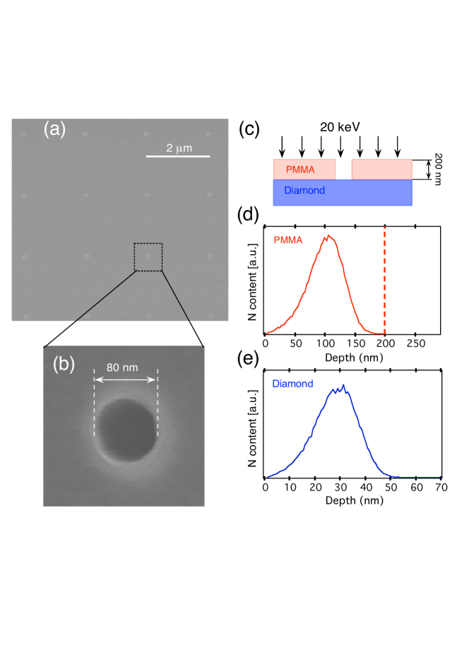
We used an ultra-pure CVD-grown single-crystal diamond with an intrinsic nitrogen content much below 1 ppb Tallaire_DRM_2006 , ensuring that each detected NV center can be faithfully attributed to an implanted nitrogen impurity Naydenov_APL_2010 . After acid cleaning of the sample, a 200 nm thick layer of PMMA A4 was deposited on the diamond surface by spin-coating. Arrays of 80 nm diameter apertures were then patterned on the PMMA layer using a 80 kV-2.3 nA electron beam lithography equipment (Nanobeam-Ltd). The apertures were regularly spaced with a m pitch array. After electron beam lithography, the mask was finally developed using MIBK/IPA. It resulted in an array of apertures with controlled spacing and diameter, as shown in Fig. 1 (a) and (b). This process, which simply relies on the deposition of a PMMA resist and patterning using electron beam lithography, prevents from any damage of the diamond substrate, as compared to other methods like plasma etching or carving with a focused ion beam.

III Implantation
Nitrogen was then implanted from a CN- molecular ion beam with 40 keV kinetic energy. When a CN- molecule hit the surface, it broke in two parts. Taking into the mass selection in the ion beam, it then became equivalent to a joint implantation of nitrogen 14N and carbon 12C with respective energies about 20 keV and 18 keV. As shown in Fig 1 (d) and (e), a SRIM simulation Ziegler_SRIM indicates that the nitrogen atoms will stop at an approximate depth of nm below the diamond surface, whereas they are stopped by the PMMA layer in the masked parts of the sample (see Fig. 1 (c)). The evaluated straggling was about 9 nm, much smaller than the diameter of the aperture. Note that the simultaneous braking of the nitrogen and carbon atoms as they penetrate into the diamond will increase the number of vacancies created close to the implanted nitrogen atoms, thus helping in the formation of the NV centers Naydenov_APL_2010 .
The toxic CN- molecules were in situ produced with a negative sputter ion source. Cs ions were used to sputter a target consisting of a mixture of BN and graphite powders and reaction in the plasma generated above the target led to the creation of CN- molecules among other species. In this ion source which was initially developed for tandem accelerator, the negatively charged ions were only produced in their single charged state. This effect decreased the number of possible ions corresponding to a given energy-mass product, providing an easy identification of a given ion which selection was realized by a double focused magnet. The sorted ions were then accelerated to an adjustable kinetic energy ranging from a few keV to hundreds of keV. The output of the accelerator is equipped with an implantation setup consisting of an electrostatic scanning system and a specifically designed chamber with secondary electron suppression Ion_Channeling .
After the implantation run corresponding to an applied dose of ions/cm2 with a current of 600 nA, the PMMA layer was removed by acid treatment. The sample was then annealed at C for 2 hours to induce vacancy diffusion leading to the conversion of the implanted nitrogen atoms into luminescent NV color centers.
IV Optical characterization of the implanted sample
The photoluminescence (PL) properties of the implanted and annealed sample were then studied using a home-made scanning confocal microscope. A laser operating at 532 nm wavelength was focused onto the sample through an oil immersion microscope objective. The PL was collected by the same objective, spectrally filtered from the remaining excitation laser light, and focused onto a m diameter pinhole. The PL was finally directed to avalanche photodiodes working in photon counting regime.
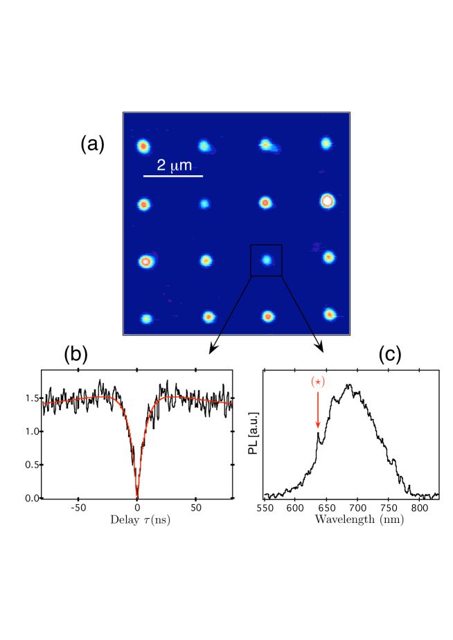
A typical PL raster scan of the sample is shown in Fig. 2 (a), displaying an array of photoluminescent spots which matches the PMMA mask with its period of drilled holes. This observation clearly demontrates the efficiency of the implantation technique.
In order to infer the number of emitters associated to each luminescent spot, we performed a photon correlation measurement using a Hanbury Brown and Twiss interferometer. Following the procedure of Ref. Brouri_OptLett_2000 for background correction and normalization to shotnoise level, the histogram of the time delays between two consecutive photon detections is equivalent to the second-order autocorrelation function of the luminescence intensity emitted by the analyzed spot. Fig. 2 (b) and (c) respectively show the photon correlation measurement and the spectral analysis associated to the circled spot in Fig. 2 (a). The dip observed at zero delay in the function is the signature of a single emitter located in the corresponding implanted area. Complementary spectral analysis showed that most of the observed emitters were of the negatively-charged state NV-. Note that in our case of shallow implantation, the remaining defects of neutral charge state NV0 could be efficiently transformed into their counterpart NV- by surface oxidation, as shown in Ref. Santori_APL2010 .

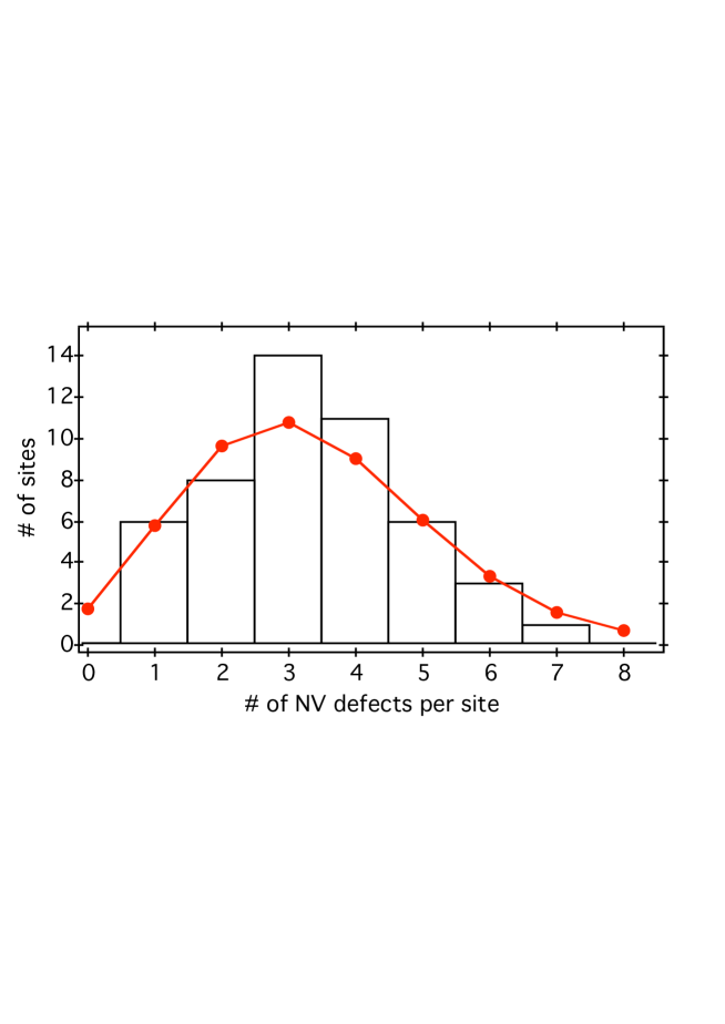
The number of emitting NV defects in the implanted spots was finally determined from combined measurements of the depth of the zero-delay dip in the function, and of the luminescence intensity compared to the mean level corresponding to a single NV emitter. The corresponding histogram is shown in Fig. 3. Since the number of implanted ions is random, we obtained a broad distribution which can be fitted by a Poissonian distribution with a mean value equal to . Since the irradiation dose corresponds to approximately 50 nitrogen atoms per spot, the conversion yield of implanted nitrogen ions into NV defects is near 0.07. As expected from the joint implantation of carbon atoms associated to the the CN- molecular beam, this value is more than two times higher than the reported ones for low-energy nitrogen implantation Rabeau_APL_2006 ; Pezzagna_NJP_2010 .

V Conclusion
In conclusion, we showed that arrays of NV color centers can be reliably produced by implanting CN- molecules through the 80 nm diameter holes in a PMMA mask of 200 nm thickness which was deposited on top of a single-crystal diamond sample. The joint implantation of carbon increased the conversion of the implanted nitrogen atoms into NV centers. The apertures and the thickness of the PMMA layer have to be optimized in order to improve the resolution of the implanted impurities but fabrication of patterns below 10 nm have already been reported in thinner PMMA layers Vieu_AppliedSurfaceScience_2000 . This flexible technique holds therefore strong promise for building scalable quantum registers based on coupled spins.
VI Acknowledgements
We are grateful to Géraldine Dantelle for processing the diamond sample after the implantation run, and we thank Fedor Jelezko for helpful discussions. Work done at LPQM was partially sponsored by the DIAMAG project of Agence Nationale de la Recherche. During the writing of our manuscript, we have been aware of a related work reporting nitrogen implantation through an array of apertures in an electron beam lithography resist Awschalom_Nanoletters_2010 .
References
- (1) A. Gruber, A. Drabenstedt, C. Tietz, L. Fleury, J. Wrachtrup, and C. von Borczyskowski, “Scanning confocal optical microscopy and magnetic resonance on single defect centers”, Science 276, 2012 (1997).
- (2) R. Alléaume, F. Treussart, G. Messin, Y. Dumeige, J.-F. Roch, A. Beveratos, R. Brouri-Tualle, and P. Grangier, “Experimental open air quantum key distribution with a single photon source”, New J. Phys. 6, 92 (2004).
- (3) F. Jelezko, T. Gaebel, I. Popa, A. Gruber, and J. Wrachtrup, “Observation of coherent oscillations in a single electron spin”, Phys. Rev. Lett. 92, 076401 (2004).
- (4) P. Neumann, R. Kolesov, B. Naydenov, J. Beck, F. Rempp, M. Steiner, V. Jacques, G. Balasubramanian, M. L. Markham, D. J. Twitchen, S. Pezzagna, J. Meijer, J. Twamley, F. Jelezko, and J. Wrachtrup, “Quantum register based on coupled electron spins in a room-temperature solid”, Nat. Phys. 2010, 6, 249.
- (5) T. M. Babinec, B. J. M. Hausmann, M. Khan, Y. Zhang, J. R. Maze, P. R. Hemmer, and M. Lončar, “A diamond nanowire single-photon source”, Nature Nanotech. 5, 195 (2010).
- (6) R. Esteban, T. V. Teperik, and J. J. Greffet, “Optical patch antennas for single photon emission using surface plasmon resonances”, Phys. Rev. Lett. 104, 026802 (2010).
- (7) F. Treussart, V. Jacques, E Wu, T. Gacoin, P. Grangier, and J.-F. Roch, “Photoluminescence of single colour defects in 50 nm diamond nanocrystals”, Physica B 376, 926 (2006).
- (8) E. Ampem-Lassen, D. A. Simpson, B. C. Gibson, S. Trpkovski, F. M. Hossain, S. T. Huntington, K. Ganesan, L. C. L. Hollenberg, and S. Prawer, “Nano-manipulation of diamond-based single photon sources”, Opt. Express 17, 11287 (2009).
- (9) T. van der Sar, E. C. Heeres, G. M. Dmochowski, G. de Lange, L. Robredo, T. H. Oosterkamp, and R. Hanson, “Nanopositioning of a diamond nanocrystal containing a single nitrogen-vacancy defect center”, Appl. Phys. Lett. 94, 173104 (2009).
- (10) M. Barth, N. Nsse, B. Lchel, and O. Benson, “Controlled coupling of a single-diamond nanocrystal to a photonic crystal cavity”, Opt. Lett. 34, 1108 (2009).
- (11) G. Balasubramanian, P. Neumann, D. Twitchen, M. Markham, R. Kolesov, N. Mizuochi, J. Isoya, J. Achard, J. Beck, J. Tissler, V. Jacques, P. R. Hemmer, F. Jelezko, and J. Wrachtrup, “Ultralong spin coherence time in isotopically engineered diamond”, Nat. Mater. 8, 8, 383 (2009).
- (12) J. Tisler, G. Balasubramanian, B. Naydenov, R. Kolesov, B. Grotz, R. Reuter, J.-P. Boudou, P. A. Curmi, M. Sennour, A. Thorel, M. Borsch, K. Aulenbacher, R. Erdmann, P. R. Hemmer, F. Jelezko, and J. Wrachtrup, “Fluorescence and spin properties of defects in single digit nanodiamonds”, ACS Nano 3, 1959 (2009).
- (13) J. Meijer, B. Burchard, M. Domhan, C. Wittmann, T. Gaebel, I. Popa, F. Jelezko, and J. Wrachtrup, “Generation of single color centers by focused nitrogen implantation”, Appl. Phys. Lett. 87, 261909 (2005).
- (14) J. R. Rabeau, P. Reichart, G. Tamanyan, D. N. Jamieson, S. Prawer, F. Jelezko, T. Gaebel, I. Popa, M. Donham, and J. Wrachtrup, “Implantation of labelled single nitrogen vacancy centers in diamond using 15N”, Appl. Phys. Lett. 87, 261909 (2005).
- (15) T. Gaebel, M. Domhan, I. Popa, C. Wittmann, P. Neumann, F. Jelezko, J. R. Rabeau, N. Stavrias, A. D. Greentree, S. Prawer, J. Meijer, J. Twamley, P. R. Hemmer, and J. Wrachtrup, “Room-temperature coherent coupling of single spins in diamond”, Nature Phys. 2, 408 (2006).
- (16) T. Vogel, J. Meijer, A. Stephan, U. Weidenmuller, U. Dagkaldiran, S. Kubski, P. Baving, H. W. Becker, and H. Rocken, “Ion beam synthesis of buried CoSi2-structures”, Nucl. Instrum. Methods Phys. Rev. B 188, 174 (2002).
- (17) C. D. Weis, A. Schuh, A. Batra, A. Persaud, J. Bokor, C. C. Lo, S. Cabrini, G. D. Fuchs, R. Hanson, D. D. Awschalom, and T. Schenkel, “Single atom doping for quantum device development in diamond and silicon”, J. Vac. Sci. Technol. B 26, 2596 (2008).
- (18) J. Meijer, S. Pezzagna, T. Vogel, B. Burchard, H. H. Bukow, I. W. Rangelow, Y. Sarov, H. Wiggers, I. Plmel, F. Jelezko, J. Wrachtrup, F. Schmidt-Kaler, W. Schnitzler, and K. Singer, “Towards the implanting of ions and positioning of nanoparticles with sub-nm resolution”, Applied Physics A 91, 567 (2008).
- (19) W. Schnitzler, N. M. Linke, R. Fickler, J. Meijer, F. Schmidt-Kaler, and K. Singer, “Deterministic ultracold ion source targeting the Heisenberg limit”, Phys. Rev. Lett. 102, 070501 (2009).
- (20) A. Tallaire, A. T. Collins, D. Charles, J. Achard, R. Sussmann, A. Gicquel, M. E. Newton, A. M. Edmonds, and R. J. Cruddace, “Characterisation of high-quality thick single-crystal diamond grown by CVD with a low nitrogen addition”, Diamond Related Mater. 15, 1700 (2006).
- (21) B. Naydenov, V. Richter, J. Beck, M. Steiner, P. Neumann, G. Balasubramanian, J. Achard, F. Jelezko, J. Wrachtrup, and R. Kalish, “Enhanced generation of single optically active spins in diamond by ion implantation”, Appl. Phys. Lett. 96, 163108 (2010).
- (22) J. F. Ziegler, “SRIM-2003”, Nucl. Instrum. Methods Phys. Res. B 219-220, 1027 (2004).
- (23) The implantation chamber is tilted at in order to avoid ion beam channeling which could induce an increase of the ion penetration depth compared to the SRIM prediction. The efficiency of the design was controlled by an independent SIMS measurement which gave a derivation below in dose and depth for a silicon sample implanted with 60 keV B+ ions.
- (24) R. Brouri, A. Beveratos, J.-P. Poizat, and P. Grangier, “Photon antibunching in the fluorescence of individual color centers in diamond”, Opt. Lett. 25, 1294 (2000).
- (25) K. M. C. Fu, C. Santori, P. E. Barclay, and R. G. Beausoleil, “Conversion of neutral nitrogen-vacancy centers to negatively charged nitrogen-vacancy centers through selective oxidation”, Appl. Phys. Lett. 96, 121907 (2010).
- (26) S. Pezzagna, B. Naydenov, F. Jelezko, J. Wrachtrup, and J. Meijer, “Creation efficiency of nitrogen-vacancy centres in diamond”, New J. Phys. 12, 065017 (2010).
- (27) C. Vieu, F. Carcenac, A. Pépin, Y. Chen, M. Mejias, A. Lebib, L. Manin-Ferlazzo, L. Couraud, and H. Launois, “Electron beam lithography: resolution limits and applications”, Appl. Sur. Sci. 164, 111 (2000).
- (28) D. M. Toyli, C. D. Weis, G. D. Fuchs, T. Schenkel, and D. D. Awschalom, “Chip-scale nanofabrication of single spins and spins arrays in diamond”, Nano Lett. advanced online publication (2010) – http://pubs.acs.org/doi/abs/10.1021/nl102066q, arxiv:1007.0240.