Fabrication and Characterization of Topological Insulator Bi2Se3 Nanocrystals
Abstract
In the recently discovered class of materials known as topological insulators, the presence of strong spin-orbit coupling causes certain topological invariants in the bulk to differ from
their values in vacuum. The sudden change of invariants at
the interface results in metallic, time reversal invariant
surface states whose properties are
useful for applications in spintronics and quantum computation. However, a key challenge is to fabricate these materials on the nanoscale appropriate for devices and probing the surface. To this end we have produced 2 nm thick nanocrystals of the topological insulator Bi2Se3 via
mechanical exfoliation. For crystals thinner than 10 nm we observe the emergence of an additional mode
in the Raman spectrum. The emergent mode intensity together with
the other results presented here
provide a recipe for production and thickness characterization of Bi2Se3 nanocrystals.
Topological metallic surface states are predicted to have numerous properties that are useful for spintronics and quantum computation.moore ; Zhang (2009)
A challenging aspect of this research has been to isolate surface state contributions to the measured properties of topological insulators Peng (2010); Eto (2010); Analytis et al. (2010); Zhang et al. (2009); Park et al. (2010). Studying nanometer thick crystals allows one to tune the chemical potential with electric fieldShahil et al. (2010); Teweldebrhan et al. (2010); Ding et al. (2009); Sakamoto et al. (2010); Checkelsky et al. (2010), as well as observe modifications of the excitation spectrum produced by interactions of top and bottom surfacesLinder et al. (2009); Liu et al. (2010); Lu et al. (2010); Zhang et al. (2010); Sakamoto et al. (2010).
One option for producing thin crystals is mechanical exfoliation. This method, together with Raman spectroscopy, has proven to be
extremely fruitful in the study of
grapheneGupta et al. (2006); Kuzmenko et al. (2009) and other nanocrystals Malard et al. (2009); Sandilands et al. (2010). Indeed, Raman provides direct access to the phonon spectrum and can be used to map the
thicknessGupta et al. (2006); Yoon et al. (2009)
or doping levelBasko et al. (2009)
over a large area.
Similar studies of the topological insulators Bi2Se3 and
Bi2Te3 have been attempted. To date, these
experiments have been limited to exfoliated Bi2Se3
crystals 10 nm thickSteinberg et al. (2010); Checkelsky et al. (2010); morpurgo or
Bi2Te3 where the bulk gap is
smallShahil et al. (2010); Teweldebrhan et al. (2010). A limiting
factor in these experiments was the strong optical absorption of
these compounds, making the identification of thin crystals
difficult on Si/SiO2 substrates. With this in
mind, we have mechanically exfoliated Bi2Se3 crystals on
Mica, enabling us to optically identify crystals only 2 nm thick.
By systematically studying these crystals with Raman spectroscopy and
optical and atomic force microscopies (AFM) we have devised a method for
characterizing the thickness of Bi2Se3 nanocrystals using
non-invasive, all-optical methods. Specifically, an
additional mode appears in the Raman spectra for ultrathin ( 10 nm)
crystals. The observed thickness dependence of the emergent mode intensity
can be used for thickness verification of nanocrystals via Raman
measurements.
Bi2Se3 forms a rhombohedral lattice in which the unit cell is composed of
three five-layer stacks known as quintuple layers (QL). A unit
cell measures 2.87 nm along the axis, and 1 QL is 0.96 nm
thick.Richter and Becker (1977) Atoms are arranged into
planar hexagonal sheets with the sequence
-[Se(2)-Bi-Se(1)-Bi-Se(2)]- sup1 .
The superscripts indicate the structural in-equivalence of the
Se ions, with the Se(1) atom at a center of inversion within
a QL. Therefore one expects phonon modes to be exclusively
infrared (IR) or Raman active. The weak van der Waals
bonds between neighboring Se(2) planes enables mechanical exfoliation. Ultrathin Bi2Se3 nanocrystals could be identified after
exfoliation by optical microscopy in transmission mode. The crystal thickness was subsequently determined using AFMsup1 .
Raman spectroscopy ( = 532 nm, spot size 1 m) confirmed that these
nanocrystals are indeed Bi2Se3 and was used to study the
evolution of the crystal lattice structure with thickness.
A raman spectrum () for a bulk
crystal is shown in Fig. 1a, where we observe a strong
phonon mode at 175 cm-1 and the onset of a mode below 150
cm-1. Previous resultsRichter and Becker (1977) suggest the higher energy mode
corresponds to a Raman active A1g mode and the latter to an
Eg mode, in accord with group theory predictions for
phonons at the Brillouin zone center (q = 0) probed by optical
experiments. Indeed, the 5 atoms in the unit cell should lead to
12 optical modes, each of which is either exclusively Raman or infrared activeRichter and Becker (1977). We also observe a broad shoulder between
200-350 cm-1, similar to a feature observed in a recent IR study of bulk
Bi2Se3 (see Fig.2b).2010PhRvB..81l5120L The presence of
this feature in both Raman as well as IR and its broad lineshape suggest that it is due to two-phonon excitations.
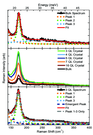
To quantitatively analyze the evolution of the spectra, we
fit the measured Raman data with multiple Lorentzian oscillators in the form:
where ranges from 1 to 3 or 4,
depending on thickness, accounts for the background,
is the center, is the width, and is the area of peak . The resulting fit
for the bulk spectrum with three oscillators is shown in Fig.
1a, where the center frequency of the Eg mode
(Peak 1) was fixed at 131.5 cm-1 based on previous
studiesRichter and Becker (1977). Turning to Fig. 1b we
examine the evolution of the Raman spectra with varying crystal
thicknesses, where an enhancement of the overall signal is observed with decreasing number of QL. As is
discussed below this enhancement results from multiple
reflections in the Bi2Se3 crystal. Perhaps more surprisingly, an additional mode
emerges at 158 cm-1 as the crystal thickness is reduced (see Fig. 1c). Indeed, the use of
only three oscillators, which worked well for crystals thicker
than 10 QL (Fig. 1a), results in a large difference
around 158 cm-1 between the fit (dashed dotted line) and the spectrum.
By simply adding another mode (), the
fit (solid line) agrees very well with the data.
The emergence of the mode at 158 cm-1 for ultrathin crystals suggests it can be used to verify sample thickness.
We explore this possibility in Fig. 2, where we plot the ratio of the emergent mode intensity with the main peak intensity (). For thicknesses below 10 QL this ratio increases and agrees well with behavior (dashed line), which corresponds to the relative weight of surface and bulk modes. Indeed, the intensity of a particular mode is proportional to the volume over which the light can emanate. For a surface mode, this volume is independent of thickness. In contrast, for a bulk mode the volume probed is proportional to the crystal thickness (for thicknesses less than the penetration depth). Unfortunately, due to the detection limit of our instrument, we are not able to convincingly detect the mode for A4/A2 0.02.
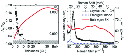
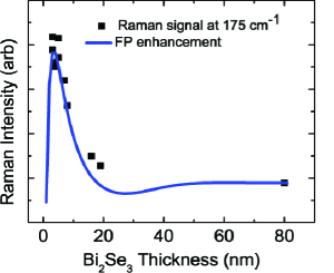
While the mode appears to have its origin in the surface, it could also be due to Fabry-Perot (FP) interference in the Mica substrate. To rule this out, we repeatedly performed Raman spectroscopy on a single 3 QL nanocrystal and subsequently cleaved the back surface of the Mica to reduce its thickness. The resultant spectra all overlapped (not shown), implying that FP interference in the Mica substrate can be neglected. Nonetheless, for a fixed substrate thickness, the interference effects due to multiple reflections in the Bi2Se3 nanocrystals will change as the crystals are thinned. To check the FP effects on the Raman spectra we have performed a calculation similar to the one shown to work well in graphene and Bi2Sr2CaCu2O8 nanocrystals.Yoon et al. (2009); Sandilands et al. (2010) In Fig. 3, we plot the measured and the calculated intensity (FP model) as a function of crystal thickness for the main mode (175 cm-1). Changes in the ratio () due to FP effects are plotted in Fig. 2a and only reveals a very small dependency on crystal thickness, which is opposite to what we observe. Therefore, the emergent mode is intrinsic to Bi2Se3 nanocrystals and not caused by FP effects. However, Fig.3 shows that the change in the overall Raman signal with crystal thickness is explained by FP interference effects only if the optical constants are modified from the bulk values. This modification is not unreasonable given recent photoemission experimentsZhang et al. (2010); Liu et al. (2010). Interestingly, these data also show the utility of Raman measurements, as the overall intensity can be used to determine the thickness of the Bi2Se3 nanocrystals.
While the FP interference described above can account for the overall intensity-thickness trends in Fig. 1, the origin of the 158 cm-1 mode remains unclear. Interestingly, an additional mode also appeared in Raman spectra of nanocrystals of the isostructural topological insulator Bi2Te3.Shahil et al. (2010) This mode matched perfectly the frequency of an infrared-active mode and so it was attributed to the breaking of inversion symmetry. Shahil et al suggested that mechanical exfoliation resulted in breaks within a QL as well as between them. A similar explanation may be appropriate for Bi2Se3: a recent IR reflectance study of the bulk revealed a mode with the same frequency and width2010PhRvB..81l5120L (see Fig.2b). However, in Bi2Te3 this mode appeared in crystals thinner than 84 nm, whereas it only appears in Bi2Se3 nanocrystals thinner than 10 nm. We believe the mode may be due to the built-in electric fields at the surface. Specifically, the band bending inherent to materials with surface states will generate asn electric field that will break the inversion symmetry.
We have shown that Raman spectroscopy is an effective
nanometrology tool for identifying nanocrystals of the topological
insulator Bi2Se3. This is accomplished by monitoring i) the overall intensity of the Raman signal and/or ii) the strength of the emergent mode at 158 cm-1. The overall thickness dependence of
the intensity can be accounted for by proper modeling of the
effect of interference on the Raman spectra.
The origin of the emergent mode remains unclear, although the presented optical conductivity data suggests that inversion symmetry breaking leads to an IR mode becoming Raman active. However, it is interesting to note that the emergent mode appears for the same thickness regime of Bi2Se3 for which a gap has been theorized to open due to coupling of the two surfaces. Liu et al. (2010); Zhang et al. (2010) In addition, the polar surface of Mica
may lead to band bending, which breaks inversion symmetry.
Therefore performing Raman spectroscopy on a suspended crystal
would provide conclusive determination of the influence of the
Mica substrate on the Bi2Se3 nanocrystals. Nonetheless, we
have provided a path for fabricating and identifying Bi2Se3
nanocrystals through the combination of mechanical exfoliation on
transparent substrates and the use of Raman spectroscopy. This work paves
the way for future devices and studies of the surface states of
topological insulators.
We are grateful for numerous discussions with Y.B. Kim and H.Y. Kee and we thank Y. J. Choi for the transport measurement. Work at the University of Toronto was supported by NSERC, CFI, and ORF; work at Rutgers University was supported by the NSF under grant NSF-DMR-0804109.
- (1) J. Moore Nat. Phys., 5, 378 (2009)
- Zhang (2009) H, Zhang, C. Liu, X. Qi, X.Dai, Z. Fang, S. Zhang, Nature Phys.,5, 438–442 (2009) and references therein
- Peng (2010) H. Peng, K. Lai, D. Kong, S. Meister, Y. Chen, X.-L. Qi, S.-C. Zhang, Z.-X. Shen, Y. Cui, Nature Mat., 9, 225 (2010)
- Eto (2010) K. Eto, Z. Ren, A. A. Taskin, K. Segawa, Y. Ando Phys. Rev. B, 81, 195309 (2010)
- Analytis et al. (2010) J. G. Analytis, J.-H. Chu, Y. Chen, F. Corredor, R. D. McDonald, Z. X. Shen, I. R. Fisher Phys. Rev. B, 81, 205407 (2010)
- Zhang et al. (2009) T. Zhang, P. Cheng, X. Chen, J.-F. Jia, X. Ma, K. He, L. Wang, H. Zhang, X. Dai, Z. Fang, X. Xie, Q.-K. Xue, Phys. Rev. Lett., 103, 266803 (2009)
- Park et al. (2010) S. R. Park, W. S. Jung, C. Kim, D. J. Song, C. Kim, S. Kimura, K. D. Lee, N. Hur, Phys. Rev. B, 81, 041405 (2010)
- Shahil et al. (2010) K. M. F. Shahil, M. Z. Hossain, D. Teweldebrhan, A. A. Balandin, Appl. Phys. Lett., 96, 153103 (2010)
- Teweldebrhan et al. (2010) D. Teweldebrhan, V. Goyal, A. A. Balandin Nano Lett., 10, 1209 (2010)
- Ding et al. (2009) Z. Ding, S. K. Bux, D. J. King, F. L. Chang, T.-H. Chen, S.-C. Huang, R. B.Kaner, Journal of Mat. Chem., 19, 2588 (2009)
- Sakamoto et al. (2010) Y. Sakamoto, T. Hirahara, H. Miyazaki, S.-i. Kimura, S. Hasegawa, Phys. Rev. B, 81, 165432 (2010) and references therein
- Checkelsky et al. (2010) J. G. Checkelsky, Y. S. Hor, R. J. Cava, N. P. Ong, arXiv (2010), arXiv:1003.3883v1 cond-mat.mes-hall
- Linder et al. (2009) J. Linder, T. Yokoyama, A. Sudbø, Phys. Rev. B, 80, 205401 (2009)
- Liu et al. (2010) C.-X. Liu, H. Zhang, B. Yan, X.-L. Qi, T. Frauenheim, X. Dai,; Z. Fang, S.-C. Zhang, Phys. Rev. B, 81, 041307 (2010)
- Lu et al. (2010) H.-Z. Lu, W.-Y. Shan, W. Yao, Q. Niu, S.-Q. Shen, Phys. Rev. B, 81, 115407 (2010)
- Zhang et al. (2010) Y. Zhang, K.He, C-Z. Chang, C-L. Song, L-L. Wang, X. Chen, J-F. Jia, Z. Fang, X. Dai, W-Y. Shan, S-Q. Shen, Q. Niu, X-L. Qi, S-C. Zhang, X-C. Ma and Q-K. Xue, Nature Phys., 6, 584 (2010)
- Gupta et al. (2006) A. Gupta, G. Chen, P. Joshi, S. Tadigadapa,; P.C. Eklund, Nano Lett., 6, 2667 (2006)
- Kuzmenko et al. (2009) A. B. Kuzmenko, L. Benfatto, E. Cappelluti, I. Crassee, D. van der Marel, P. Blake, K. S. Novoselov, A. K. Geim, Phys. Rev. Lett., 103, 116804 (2009) and references therein
- Malard et al. (2009) L. M. Malard, , M. A. Pimenta G. Dresselhaus, M. S. Dresselhaus, Phys. Rep., 473, 51 (2009)
- Sandilands et al. (2010) L. J. Sandilands, J. X. Shen, G. M. C. F. Zhao, S. Ono, Y. Ando, K. S. Burch, Phys. Rev. B, 82, 064503 (2010)
- Yoon et al. (2009) D. Yoon, , H. Moon, Y.-W. Son, J. S. Choi, B. H. Park, Y. H. Cha, Y. D. Kim, H. Cheong, Phys. Rev. B, 80, 125422 (2009)
- Basko et al. (2009) D. M. Basko, S. Piscanec, A. C. Ferrari, Phys. Rev. B, 80, 165413 (2009) and references therein
- Steinberg et al. (2010) H. Steinberg, D. R. Gardner, Y. S. Lee, P.Jarillo-Herrero, eprint arXiv, 1003, 3137 (2010)
- (24) B. Sacepe, J.B. Oostinga, J. Li, A. Ubaldini, N.J.G. Couto, E. Giannini, A.F. Morpurgo, arXiv:1101.2352v1 [cond-mat.mes-hall], (2011)
- Richter and Becker (1977) W. Richter, C. R. Becker, Phys. Stat. Sol. (b), 84, 619 (1977)
- (26) See supplementary material at http://dx.doi.org/10.1063/1.3573868 for the crystal structure of Bi2Se3 and an AFM image and the thickness determination.
- (27) A. D. Laforge, A. Frenzel, B. C. Pursley, T. Lin, X. Liu, J. Shi, D. N. Basov, Phys. Rev. B, 81, 125120 (2010)