On the inner Double-Resonance Raman scattering process in bilayer graphene
Abstract
The dispersion of phonons and the electronic structure of graphene systems can be obtained experimentally from the double-resonance (DR) Raman features by varying the excitation laser energy. In a previous resonance Raman investigation of graphene, the electronic structure was analyzed in the framework of the Slonczewski-Weiss-McClure (SWM) model, considering the outer DR process. In this work we analyze the data considering the inner DR process, and obtain SWM parameters that are in better agreement with those obtained from other experimental techniques. This result possibly shows that there is still a fundamental open question concerning the double resonance process in graphene systems.
pacs:
63.20.D-, 63.20.kd, 63.22.Rc, 73.22.PrIn recent years, the physics of monolayer graphene has been thoroughly investigated, unveiling a wealth of interesting and unusual properties, most of which are related to graphene’s distinct electronic properties, that consist of a linear and isotropic dispersion of the electronic states around the Fermi level () near the K point in the Brillouin zone (BZ). Bilayer graphene is also a very interesting material. While in the unbiased bilayer the valence and conduction bands touch each other at the Fermi level, a gap can be opened and tuned, for example, by the application of an external electric field gava09 ; ando09 ; kuzmenko09 ; malardprl08 ; pinczuk09 ; malardreport , which makes this a promising system for the fabrication of nanoelectronic devices. The development of bilayer-graphene-based bulk devices depends on the detailed understanding of its electronic properties. Since the unit cell of AB stacked bilayer graphene is the same as that of graphite, one can model the bilayer electronic structure using a tight-binding (TB) model for graphite wallace47 , by adapting the Slonczewski-Weiss-McClure (SWM) parameterization McClure1957 ; SW1958 of relevant couplings. There are several theoretical mim07 ; partoens06 ; gruneis08 and experimental li09 ; zhang08 ; mafra09 ; lmalard07 ; kuzmenko09 ; malardphysstatsol studies of theses SWM parameters, but the agreement between the reported values, obtained with different experimental techniques, is not entirely satisfactory.
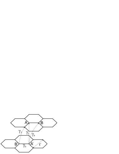
In previous resonance Raman studies of bilayer graphene lmalard07 ; mafra09 in our group, the dispersion of the G′ Raman band (also called 2D band) as a function of the laser energy was measured, and the nearest-neighbor hopping parameters , , and (shown in Fig. 1) were determined. In Ref.mafra09, , the fitting included also the in-plane second-neighbor hopping parameter , which is expected to be of the same order as the out-of-plane nearest-neighbor parameters. The parameter , which represents the difference between the on-site energies of the sublattices A and B, was also taken into account.
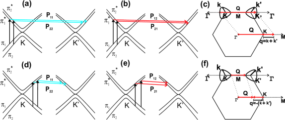
Group theory analysis for bilayer graphene predicts four distinct DR processes (P11, P22, P12, and P21) along the KM direction, which are illustrated in Fig. 2. The triangularly-shaped isoelectronic curves around the K and K′ points in Figs. 2(c) and 2(f) are the equienergy contours of the electrons involved in the scattering process. The value of the equienergy determined by the laser energy , that creates the electron-hole excitations is the first step of the DR process, as shown in Figs. 2(a-b) and 2(d-e). The analysis of the data in Refs. lmalard07, and mafra09, was done considering a double resonance (DR) process involving only backscattering of electronic states along the K line with phonons along the KM line, a process we call the outer DR Raman process. From this analysis, we were able to obtain the SWM parameters, but our values for the and were found to be smaller than those determined using other experimental techniques.
This restricted one-dimensional analysis of the DR process rests on the following assumptions: (i) that a one-dimensional integration along the KM direction captures the essential features of the DR process, as found in Ref. maultzsch04b, ; (ii) that some of the graphically determined double-resonant vectors, related to forward-scattering processes [connecting points on the electronic equienergy curves surrounding points K and K′ in Fig. 2(c)], vanish by destructive interference, as found also in Ref. maultzsch04b, ; (iii) that, by plotting the phonon density of states (PDOS) of graphene satisfying the DR process bob07 , one can identify a strong singularity at the phonon q-vector involved in the outer process, and a much smaller PDOS value for the phonon q-vector along the K line that backscatters an electronic state along the KM line, and also meets the DR condition, in a process we refer to as the inner process. This is the reason why attention is usually paid solely to the one-dimensional outer process bob07 ; K rti2002 ; Ferrari2006 . While the analysis in Ref. maultzsch04b, did consider both outer and inner processes, and the calculation of the Raman cross section considered all possible resonant and non-resonant processes, a critical approximation was employed: the matrix elements involved, related to electron-photon and electron-phonon couplings, were assumed to be constant and independent of the wavevectors k and q of the electrons and phonons, respectively.
This state of affairs indicates that some of the conventional wisdom related to the DR process in graphene-based systems needs to be reevaluated. In the present work, we address the particular issue of the preponderance of the outer process. This may be particularly important in the context of symmetry-breaking potentials imposed on the graphene system. For example, if a compressive or tensile strain is applied to the system, either intentionally or due to interaction with a substrate, one expects the doubly degenerate G′ peaks to split into two sub-bands G and G, due to the movement of the Dirac cones and consequently the breaking of the symmetry of the DR Raman process. We reanalyze the data reported in Ref. mafra09, considering now the inner DR process, in which the electronic excitations involved are along the KM line and the phonons are along the K line. As discussed below, we obtain a very good fit of the experimental results using the same values for the parameters , , , and as in the outer-process case, but with values for and which are in better agreement with those obtained from other experimental techniques.
In order to understand the experimental results we obtained, it is important to build a bridge between experiment and theory. To achieve this, we must find a relation between the electronic and the phonon dispersions of bilayer graphene. The electronic dispersion of bilayer graphene can be described in terms of the standard SWM model for graphite, as mentioned above, using a TB model wallace47 . Along the K direction, this amounts to replacing the parameter in McClure’s expressions McClure1957 by: . Here is the modulus of the electronic -vector measured from the K point and Å is the in plane nearest-neighbor carbon distance. The bands in the bilayer are obtained from a TB Hamiltonian using the parameters , , , , , and . Along the high symmetry K direction, the matrix factorizes and the dispersion of the four bands are given by:
| (1) |
where ,
and
It should be noted that these expressions are similar to those found in Ref. lmalard07 , except that here we take into account, to allow for the possibility of different doping levels between the two layers, and also include a parameter for second-nearest-neighbor interactions within the same layer. For any of the Pij () processes, we seek the dependence of the phonon energy with . In the initial step of this process (electron-hole creation), the incident photon is in resonance with the excitation of the electronic state from the valence to the conduction bands at the point. In the following, we drop the vectorial notation for the - and -vectors, since we are considering only the KM direction. The laser energy can then be written as:
| (2) |
which allows us to determine the momentum of the excited electron in the process. The electron is then scattered from a state in the vicinity of the K point to a state in the vicinity of the K′ point by emitting an iTO phonon with energy
| (3) |
where depends on and . This equation uniquely determines the momentum of the scattered electron, provided that is known. The phonon energy can be computed, and is directly related to the Raman shift for a specific Pij process, obtained with a given . Physically, the difference between the outer and inner processes lies in the phonon wavevector .
As can be inferred from the geometry in Figs. 2(c) and 2(f), for the outer process, and ) for the inner process, measured from the K point. In both cases, has a maximum amplitude of approximately . The outer and inner processes have their vectors and pointing in opposite directions. Interestingly enough, this means that calculations for the inner process can be done simply by switching into and into in Eq. (1) and looking for values of satisfying Eq. (3).
Figure 3 shows the experimental data (dots) and the TB fitting results (curves) for both the outer and the inner processes. Figure 3(a)outer shows the fit considering the outer process for the DR scattering, i.e., with phonons along the KM line. The values obtained for , , , , , and are shown in Table 1(a). Note that our value of eV is slightly smaller than that usually found in the literature eV zhang08 ; li09 ; partoens06 ) from other techniques and calculations. However, the major discrepancy is in the value of eV compared to 0.30 eV found in the graphite literature gruneis08 ; dresselhaus88 ; schneider09 . Recent infrared studies in exfoliated bilayer graphene consider eV zhang08 , but this value is not extracted directly from the experiments.
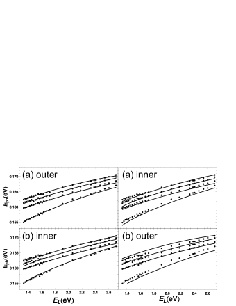
In order to theoretically compute results and compare with the experimental data in Fig. 2, we have to consider a form for the phonon energy . In this paper, we consider a nonlinear relation for the iTO phonon dispersion given by a second-order polynomial with and for the outer and inner processes respectively, as explained above. We also use two distinct non-linear phonon dispersions for the symmetric (S) and anti-symmetric (AS) branches. The best fit was obtained when we consider different dispersions for the two iTO phonon branches of bilayer graphene. Table 2 shows the parameters obtained for the S and AS phonon branches, for both scattering processes. Note that the S phonon branch is more sensitive to the change of scattering process than the AS mode.
| (a) | 3.0 | 0.35 | 0.10 | 0.18 | 0.03 | 0.10 |
|---|---|---|---|---|---|---|
| (b) | 3.0 | 0.40 | 0.30 | 0.18 | 0.03 | 0.10 |
Note also that, in Fig. 3, the fittings considering the two different DR scattering processes produce rather different results. In the inner-process case we cannot fit the data with the same parameters that produce the best fit for the outer process, shown in Fig. 3(a)outer. This is shown in Fig. 3(a)inner, where the theoretical curve obtained using the values of and from Table I(a) differs considerably from the experimental values. The best fit for the inner process is shown in Fig. 3(b)inner, with the values of eV and eV found in the literature, and with the same values of , and t′ as for the outer process. In a similar manner, the outer process cannot be fitted using the best-fit parameters for the inner-process case: deviations from the experimental results are again observed, as shown in Fig. 3(b)outer.
| symmetric | anti-symmetric | |||||
| A | B | C | A | B | C | |
| (meV) | (meVÅ) | (meVÅ2) | (meV) | (meVÅ) | (meVÅ2) | |
| (a) | 146.3 | 85.6 | -70.3 | 150.4 | 65.4 | -44.8 |
| (b) | 150 | -65.9 | -45.6 | 153.4 | -54.9 | -37 |
The above discussion shows that the inner DR process gives TB parameters in better agreement with those obtained by other experimental techniques, despite the fact that the number of phonon states with wavevectors that satisfy the DR process with visible photons is much larger for the outer DR process maultzsch04b . This result is possibly an evidence that there is still a fundamental open question concerning the double resonance selection rules in graphene.
In principle, there is a large number of phonon wavevectors that satisfy the DR process, connecting electronic states in equienergy contours around the K and K′ points. The calculation of the DR Raman profile must take into account all these possible DR phonon wavevectors, weighted by the q-vector dependence of the associated electron-phonon matrix elements. Some interference effects also appear when the Raman expression is squared out in order to calculate the Raman intensity Pimenta2007 . To our knowledge, there is only one full calculation of the shape of the Raman DR bands that takes into account the q-vector dependence of the electron-phonon matrix elements, and this calculation predicts an asymmetric shape for the DR bands in monolayer graphene Pimenta2007 . However, the experimental DR Raman bands obtained with visible photons bands are nicely fitted by a single Lorentzian lines. This possibly shows that some ingredients are missing in order to fully explain the DR process in graphene systems.
The results obtained in this paper could be the starting point to investigate other systems which constitute a hot subject in graphene physics, such as strained or twisted bilayer graphene. In the former case, bilayer graphene is grown on an insulating material (such as SiO2), which imposes a strain on the graphene system. This setup has been considered as a building block for microelectronics ni2008 . In the latter case, the stacking of the two layers is different from the usual AB (Bernal) stacking, being similar to what is found in naturally occurring and synthetic crystals presenting a variety of defects, which affect the stacking order mainly in the c-axis direction charlier1992 ; guinea2006 . In both cases, there is a significant modification in the electronic and optical properties of the systems, which directly influences the Double Raman bands. This produces different G′ peaks that can be theoretically studied by looking at the Pij processes.
Finally we hope that future experimental work on graphene systems will reveal more insights on the inner process and on scenarios where it can be considered more dominant than its counterpart, the outer process. It would also be quite fascinating if one could theoretically calculate the Raman cross section of bilayer graphene or of any of its exotic descendants such as twisted or strained graphene systems by integrating over all k points on the isoenergetic surfaces without any approximations. This might show that points other than those along the K and KM lines need to be taken into account, which might lead to a better understanding of the inner and outer processes.
This work was supported by Rede Nacional de Pesquisa em Nanotubos de Carbono - MCT, and the Brazilian Agencies CNPq and FAPEMIG. Resonance Raman studies in the near infrared range were conducted at the Center for Integrated Nanotechnologies, jointly operated by Los Alamos and Sandia National Laboratories.
References
- (1) P. Gava, M. Lazzeri, A. M. Saitta, and F. Mauri, Phys. Rev. B 79, 165431 (2009).
- (2) T. Ando and M. Koshino, J. Phys. Soc. Jpn. 78, 034709 (2009).
- (3) A. B. Kuzmenko, L. Benfatto, E. Cappelluti, I. Crassee, D. van der Marel, P. Blake, K. S. Novoselov, and A. K. Geim, Phys. Rev. Lett. 103, 116804 (2009).
- (4) L. M. Malard, D. C. Elias, E. S. Alves, and M. A. Pimenta, Phys. Rev. Lett. 101, 257401 (2008).
- (5) J. Yan, T. Villarson, E. A. Henriksen, P. Kim, and A. Pinczuk, Phys. Rrv. B 80, 241417(R) (2009).
- (6) L. M. Malard, M. A. Pimenta, G. Dresselhaus, M. S. Dresselhaus, Physics Reports 473, 51 (2009).
- (7) P. R. Wallace, Phys. Rev. 71, 622 (1947).
- (8) J. W. McClure, Phys. Rev. 108, 612 (1957).
- (9) J. C. Slonczewski and P. R. Weiss, Phys. Rev. 109, 272 (1958).
- (10) H. Min, B. Sahu, S. K. Banerjee, and A. H. MacDonald, Phys. Rev. B 75, 155115 (2007).
- (11) B. Partoens and F. M. Peeters, Phys. Rev. B 74, 075404 (2006).
- (12) A. Grüneis, C. Attaccalite, L. Wirtz, H. Shiozawa, R. Saito, T. Pichler, and A. Rubio, Phys. Rev. B 78, 205425 (2008).
- (13) Z. Q. Li, E. A. Henriksen, Z. Jiang, Z. Hao, M. C. Martin, P. Kim, H. L. Stormer, and D. N. Basov, Phys. Rrv. Lett. 102, 037403 (2009).
- (14) L. M. Zhang, Z. Q. Li, D. N. Basov, and M. M. Fogler, Z. Hao and M. C. Martin, Phys. Rev. B 78, 235408 (2008).
- (15) L. M. Malard, J. Nilsson, D. C. Elias, J. C. Brant, F. Plentz, E. S. Alves, A. H. Castro Neto, and M. A. Pimenta, Phys. Rev. B 76, 201401 (2007).
- (16) D. L. Mafra, L. M. Malard, S. K. Doorn, Han Htoon, J. Nilsson, A. H. Castro Neto, and M. A. Pimenta, Phys. Rev. B 80, 241414(R) (2009).
- (17) L. M. Malard, J. Nilsson, D. L. Mafra, D. C. Elias, J. C. Brant, F. Plentz, E. S. Alves, A. H. Castro Neto, and M. A. Pimenta, Phys. Stat. Sol. (b) 245, 2060 (2008).
- (18) J. Maultzsch, S. Reich, and C. Thomsen, Phys. Rev. B 70, 155403 (2004).
- (19) D. L. Mafra, G. Samsonidze, L. M. Malard, D. C. Elias, J. C. Brant, F. Plentz, E. S. Alves, and M. A. Pimenta, Phys. Rev. B 76, 233407 (2007).
- (20) A. C. Ferrari, J. C. Meyer, V. Scardaci, C. Casiraghi, M. Lazzeri, F. Mauri, S. Piscanec, D. Jiang, K. S. Novoselov, S. Roth, and A. K. Geim, Phys. rev. Lett. 97, 187401, (2006).
- (21) J. Kürti, V. Zólyomi, A. Grüneis, and H Kuzmany, Phys. Rev. B 65, 165433 (2002).
- (22) M.S. Dresselhaus, G. Dresselhaus, K. Sugihara, I. L. Spain and H. A. Goldberg, Carbon Fibers and Filaments, Chapter 7, Springer Verlag (Berlin Heidelberg) 1988.
- (23) J. M. Schneider, M. Orlita, M. Potemski, and D. K. Maude, Phys. Rev. Lett 102, 166403 (2009).
- (24) M. A. Pimenta, G. Dresselhaus, M. S. Dresselhaus, L. G. Cançado, A. Jorio, and R. Saito, Phys. Chem. Chem. Phys. 9, 1276-1291, (2007).
- (25) Z. H. Ni, T. Yu, Y. H. Lu, Y. Wang, Y. P. Feng, and Z. X. Shen, ACS Nano 2, 2301 (2008).
- (26) J. C. Charlier, J. P. Michenaud, and P. Lambin, Phys. Rev. B. 46, 4540 (1992).
- (27) F. Guinea, A. H. Castro Neto, and N. M. R. Peres, Phys. Rev. B. 73, 245426 (2006).