Dopant-enhanced solid phase epitaxy in buried amorphous silicon layers
Abstract
The kinetics of intrinsic and dopant-enhanced solid phase epitaxy (SPE) are studied in buried amorphous Si (-Si) layers in which SPE is not retarded by H. As, P, B and Al profiles were formed by multiple energy ion implantation over a concentration range of . Anneals were performed in air over the temperature range 460-660 oC and the rate of interface motion was monitored using time resolved reflectivity. The dopant-enhanced SPE rates were modeled with the generalized Fermi level shifting model using degenerate semiconductor statistics. The effect of band bending between the crystalline and amorphous sides of the interface is also considered.
pacs:
81.15.Aa, 81.15.Np, 61.72.TtI Introduction
Solid phase epitaxy (SPE) is an important processing step in device fabrication yet the mechanism by which atoms make the amorphous to crystalline phase transition is still poorly understood. It is known that the velocity of the crystalline-amorphous (-) interface (SPE rate) has a strong dependence on a number of parameters including pressure,Lu et al. (1990, 1991) substrate orientation,Csepregi et al. (1978) and dopant concentrationCsepregi et al. (1977a). The SPE rate in intrinsic silicon is also well described by an Arrhenius type equation with an activation energy of 2.7 eV.Roth et al. (1990)
Pioneering work on dopant-enhanced SPE was performed by Csepregi and co-workers who used ion channeling measurements to determine surface -Si layer thicknesses as a function of annealing time and temperature.Csepregi et al. (1977a) Csepregi found that the presence of impurity atoms enhanced the SPE rate up to 6 times that of the intrinsic rate for P and As and up to 20 times for B with impurity concentrations of 0.4 at.%. Further, it has been found that overlapping - and -type dopants of a similar concentration give an SPE rate close to that of an intrinsic sample, a compensation doping effect.Suni et al. (1982a) Likewise, the overlapping of two dopants of the same type gives an additive effect on the SPE regrowth rate. These electronic effects suggest that the SPE rate is sensitive to shifts in the Fermi level and that both neutral and charged defects may be responsible for the SPE process. Indeed, a number of models link the structural and electrical properties at the - interface in an attempt to describe the SPE phenomenon. Williams and Elliman (1983); Suni et al. (1982a); Lietoila et al. (1982); Mosley and Paesler (1985); Walser and Jeon (1992); Park et al. (1988); Lu et al. (1991) However, there is a significant problem with the experimental data for SPE growth of surface amorphous layers to which the SPE models have been fitted. In surface amorphous layers, the SPE rate is invariably affected by the presence of H which infiltrates the layer from the native oxide and retards the SPE growth rate.Roth et al. (1990) Roth et al. have shown that the growth rate is affected for interface depths of up to . Recent measurements also suggest that the infiltration of H can affect the dopant-enhanced SPE regrowth rate.Johnson and McCallum (2004) These findings call into question the reliability of the parameters found in previous work where SPE models have been fitted to the H-affected data.
This paper presents data for dopant-enhanced SPE kinetics in buried -Si layers. Buried -Si layers provide an environment where H concentrations at the - interface are considerably lower than the levels which have a measurable affect on SPE rates.McCallum (1996) H-free dopant-enhanced SPE data are presented for As, P, B and Al measured over a concentration range of . As-enhanced SPE data are care of McCallum. McCallum (1999) The experimental data are fitted to the generalized Fermi level shifting (GFLS) model which is one of the more highly developed models describing the dopant-enhancement effect in SPE which at this stage has not met with any significiant challenge to its validity. Lu et al. (1991) By fitting the model to SPE data for both and type impurities over a broad concentration range we are able to show that the model provides plausible values for fitting parameters which may eventually lead to the identification of the defect(s) responsible for the SPE process. In fitting the data, we have refined the GFLS model by incorporating degenerate semiconductor statistics and by endeavoring to use the most valid values and dependencies for parameters which affect semiconductor statistics. These parameters include the electron and hole effective masses and the temperature and concentration dependencies of the band gap. An extension of the model to include the effect of band bending at the - interface is discussed. Further, the scope for developing links between our data and molecular dynamics simulations of the interface motion during SPE as a possible means of identifying the mechanism giving rise to dopant-enhancement are also discussed.
In section II of this paper we provide a brief overview of the theoretical background to the GFLS model. In section III we present the experimental parameters associated with our measurements of intrinsic and dopant-enhanced SPE rates. Section IV presents the SPE rate data and fits to this data using the GFLS model and section V presents our conclusions. Details of the parameters and functional dependences used to calculate the semiconductor statistics and hence the Fermi levels in the temperature range of our SPE measurements are given in the appendix.
II Theoretical background
Atomistic SPE models have offered some insight into the rate-limiting step of the SPE process and can be used to predict the orientation dependence of the crystallisation rate through the proportionality of the growth rate with the concentration of [110] ledges. The concentration of these ledges increases with deviations away from the crystallographic direction.Csepregi et al. (1978) The shortcoming of atomistic approaches lies in their inability to predict the growth rate dependence on dopant concentration which is more likely to be explained by models based on electronic processes.
While conducting experiments on the compensation effect in the epitaxial regrowth rate of -Si, Suni et al. suggested that the bond-breaking process was mediated by vacancies that formed and migrated at the - interface.Suni et al. (1982a, b) This assumption was based on a finding by Csepregi that the activation energies of SPE regrowth and the formation of vacancies were similar.Csepregi et al. (1977b) Using the vacancy model by Van Vechten and Thurmond,van Vechten and Thurmond (1976) Suni et al. related the concentration of charged vacancies to the position of the Fermi level in the band-gap and its dependence on doping concentration. The doping concentration is proportional to the number of charged vacancies while the number of neutral vacancies is not affected. With a greater total concentration of vacancies at the interface the SPE growth rate was assumed to be enhanced via some vacancy-related bond-breaking process. The assumption that vacancies are the SPE defect has since been ruled out due to the observation of a negative activation volume for the SPE process in studies where the pressure dependence has been measured.Lu et al. (1990) However, the model was significant in that it provided a possible mechanism by which the number of growth sites at the interface could depend on doping and it related the rate-enhancement to the presence of defect energy levels within the band gap.
The charged kink-site model proposed by Williams and Elliman,Williams and Elliman (1983) is an extension of atomistic models introduced by Spaepen and Turnbull.Spaepen (1978) They considered a bond-breaking process involving the propagation of kink-like growth sites along [110] ledges. They made reference to defects associated with distorted silicon-silicon bonds being responsible for the bond-breaking process at the kink sites but did not specify the exact nature of the defects. Williams and Elliman proposed that the Fermi level on the amorphous side of the - interface would be pinned near mid-gap and that therefore the number of charged kink-related defects at the interface available to promote SPE would be governed by the doping dependence of the Fermi-level in the crystalline material. Williams and Elliman arrived at an expression for the rate-enhancement which is equivalent to: , where is the SPE rate in doped material, is the rate in intrinsic material, is the dopant concentration and is some function of temperature and is independent of . In arriving at this expression, they used parameters and functional dependencies appropriate to an extrinsic non-degenerate semiconductor and assumed that the dopants were fully ionized. At the time the model was proposed, the paucity of reliable SPE velocity data as a function of dopant concentration meant that the dopant dependence predicted by the model could not be accurately tested. Since reliable SPE data which is not affected by H has become available, it is clear that some of the simplifying assumptions which they made are not valid. However, their model still has significant merit.
Walser et al. also introduced a model based on the ideas of Spaepen and Turnbull.Walser and Jeon (1992); Park et al. (1988) The model assumes that the capture of dangling bonds (DB) at the - interface is the rate-limiting step to the SPE process and that the concentration of these defects is determined by the band structure on the amorphous side of the interface. The Fermi level is assumed to be pinned to mid gap on the amorphous side of the interface and does not affect the SPE rate. Instead, the model suggests that the concentration of DBs is changed by the doping concentration through ionization enhanced atomic mobility as per Bourgoin and Germain.Bourgoin and Germain (1975) The equations derived from this model provide reasonable fits to the data. However, the assumptions on which they are based severely limit the model’s applicability and interpretation as correctly pointed out by Lu et al.Lu et al. (1991) Namely, the law of mass action is violated when assuming that the fractional ionization of dopant atoms in -Si is independent of concentration. It should also be noted that the SPE rate data to which their model was fitted was hydrogen affected.
In their reanalysis of the Williams and Elliman charged kink site model, Lu et al. noted that for kink motion to occur, bond rearrangement must take place and that this would most likely occur via the breaking of bonds which span the - interface followed by local rearrangement and then recombination of the dangling bonds. Hence, they considered the kink site model to be a special case of the dangling bond model of Spaepen and TurnbullSpaepen (1978) in which the dangling bonds are annihilated locally and relatively quickly without taking a large number of jumps prior to annihilation. Lu et al. also reworked the electronic aspects of the charge kink site model, relaxing some of the assumptions which had been made. They called this reworked model the generalized Fermi level shifting (GFLS) model. It is this model which we have further developed by incorporating degenerate semiconductor statistics and by endeavouring to use the most valid parameters.
In the GFLS model, SPE is thought to occur via bond breaking and rearrangement at the - interface mediated by a neutral defect, , and its positively or negatively charged counterparts, . The defects may be dangling bonds or they may be some other defect. The model does not attempt to specify this. It is assumed that the defects are in thermal and electronic equilibrium and that the concentrations of are determined by the band structure and density of states (DOS) of the bulk crystal. The SPE regrowth rate is then expected to be proportional to the concentration of these defects. For an -type semiconductor and it’s intrinsic counterpart the velocities are given by
| (1a) | |||
| and | |||
| (1b) | |||
respectively, where is a constant and is the concentration of neutral defects and is independent of doping. These equations assume that for -type material, SPE is dominated by and and that each of these defects are equally capable of promoting interface motion. The charged fraction of defects is determined by Fermi-Dirac statistics and, for an -type semiconductor, is expressed as the ratio of charged to neutral defect concentrations in the crystal,
| (2) |
where is the Fermi level and represents the energy level within the band gap of the defect responsible for the SPE process. The degeneracy factor, , associated with is given by where and are the internal degeneracies of the and defect states, respectively.Bourgoin and Lannoo (1983) If a DB defect is responsible for the SPE process then it is expected that if only the spin degeneracy needs to be considered. For the positive charge state of the DB, as the degeneracy of the valence band also contributes a factor of two.
Once Eq. 2 is substituted into the expression for the velocity we obtain,
| (3) |
This equation is used to fit the normalized SPE data as a function of temperature with the degeneracy, , and the energy level, , of the SPE defect being free parameters. Lu et al. assumed that the mobilities of charged and uncharged DBs are identical.Lu et al. (1990) If the charged and neutral defect concentrations are weighted separately with a factor and in Eq. 1 then this will have the affect of weighting the degeneracy factor in Eq. 3 by a value of . The energy level of the defect predicted by the model will be unaffected by this assumption.
Figure 1 shows a schematic diagram of the Fermi level in -type Si, and intrinsic Si, over the temperature range used in this work. The energy level of the negatively charged state of the SPE defect, is assumed to track the conduction band edge, . The variation of with temperature has been exaggerated to show that it approaches the conduction band edge as the temperature decreases. As this occurs, the population of charged SPE defects, will increase as the approaches its energy level. The dopant enhanced SPE rate relative to the intrinsic rate (Eq. 3) will then be greatest for anneals performed at lower temperatures.
A shortcoming of the model is that the temperature dependence of the SPE defect energy level is not known and cannot be included in these calculations as pointed out by Lu et al.Lu et al. (1991) However, a detailed account of the model and its application to an extensive data set should provide much insight into the nature of the SPE process. Two parameters which must be calculated in order to apply Eq. 3 to normalized SPE data are and , the Fermi level of an intrinsic and doped semiconductor, respectively. This calculation and the required semiconductor parameters are outlined in the appendix.
In discussing SPE models it should also be noted that molecular dynamics (MD) simulations are also informative when attempting to identify the SPE mechanism. These simulations describe the structure and rearrangement of atoms at the - interface during SPE on a microscopic scale. Early models attributed the SPE mechanism to the motion of a dangling bond type defect.Saito and Ohdomari (1981, 1984) This defect aided the rearrangement of atoms at the interface via bond-breaking. More recently, Bernstein et al. have shown that the SPE may occur through a number of both simple and complex mechanisms.Bernstein et al. (1998, 2000) By using empirical potential simulations they have found that one simple mechanism involves the rotation of two atoms aided by coordination defects which are locally created and annihilated during crystallization. An example of a more complex mechanism involves the migration to the interface of a five-fold coordinated defect which aides the incorporation of two atoms into the crystal matrix. If the MD simulations accurately model the SPE process then doubt is cast on the generally accepted idea that SPE occurs through a single, thermally-activated process. A more complex model would probably then be needed to describe the electronic effects in SPE.
Mattoni et al. have also described the segregation and precipitation of B during SPE in highly doped Si.Mattoni and Colombo (2004) This is shown to result in the retardation of the SPE rate and is in agreement with experiment.Roth and Olson (1994) However, dopant-enhanced SPE is not considered. Indeed, all MD simulations are performed near the melting point of amorphous silicon in order to ensure reasonable simulation times. There are no MD simulations that we know of that have been performed in the temperature range considered in the present work where the effect of the dopants on the SPE rate becomes apparent (as can be seen at the lower temperatures in Fig. 7-9). If such MD simulations become possible, dopant-enhanced SPE may be understood to a greater extent on the microscopic level and could then be used to assess the applicability of the GFLS model.
III Experiment
The kinetics of dopant-enhanced SPE were measured in buried -Si layers formed by self-ion-implantation in -type, , Si(100) Czochralski grown wafers. A 1.7 MV NEC tandem ion implanter was used for all implants. During implantation, substrates were tilted off the incident beam axis to avoid channeling and affixed to the implanter stage with Ag paste to ensure good thermal contact.
To fabricate the samples, surface -Si layers were produced by forming intrinsic amorphous layers thick using the implantation schedule: and . Constant concentration profiles of P, B or Al were then created by multiple energy implantation. The expected concentration profiles calculated using the Profile codepro (.) are shown in Figs. 2-5 for As, P, B and Al, respectively. The implant schedule used to create a constant concentration profile of over a certain depth is indicated at the top of each figure. The schedule used for As implants in Ref. McCallum (1999) is shown for completeness. The implant fluences were scaled to obtain a range of peak concentrations between and . SPE rate enhancement is generally immeasurable at lower concentrations and approaches the solid solubility limit at concentrations higher than this range. The dopant concentrations were relatively constant over the depth range: 0.45-0.85, 0.5-0.8, 0.95-1.35 and 0.8-1.15 for As, P, B and Al, respectively. Preliminary secondary ion mass spectrometry (SIMS) data from P and B implanted samples compare well with the shape and depth range of these curves although a standard to calibrate the concentration axis was not obtained. SIMS on the Al doped layers was not performed. For As, RBS-C was used to compare expected and actual profiles and agreement was obtained to within 10%.
After implantation samples were annealed at C for 1 hour under UHV conditions in order to completely crystallize the layer. Buried amorphous layers were then formed by using the implantation schedule: and using a flux of . This schedule produced a buried amorphous layer 0.87 thick with a 0.3 thick -Si capping layer.
The SPE rates were determined in air using a time-resolved reflectivity (TRR) system equipped with two lasers collecting data simultaneously at and .McCallum (1996) The samples were held on a resistively heated vacuum chuck while anneals were performed over a temperature range of in increments. The temperature of the samples during the anneals was calibrated by comparing the reading of a type-K thermocouple embedded in the sample stage with the melting points of various suitably encapsulated metal films evaporated onto Si wafers. The error associated with the temperature reading was found to be C.
IV Results and Discussion
The kinetics of dopant-enhanced SPE were measured over the temperature range 460-660oC for samples containing a number of different P, B or Al concentrations in the range . These were compared to the As-enhanced SPE measurements presented in Ref. McCallum (1999) by McCallum collected on the same TRR system.
The temperature dependence of the SPE regrowth rate for intrinsic and doped buried -Si layers is shown in Fig. 6. For clarity, only one concentration for each dopant studied is plotted. Fitting an Arrhenius type equation of the form to the intrinsic SPE data yielded a velocity prefactor of /s and an activation energy of eV. The errors associated with these values were calculated by considering the 1% temperature reproducibility, the RMS noise in the determined velocity curve and the errors associated with the fitting procedure. These values compare quite well to those reported by Roth et al. for thick surface -Si layers which were Å/s and 2.7 eV.Roth et al. (1990)
The greatest - interface velocity enhancements were found for samples implanted with B. It was also found that Al concentrations greater than caused the TRR signal to collapse. This indicated that the - interface had become rough. SPE rate retardation and interface segregation has previously been observed for Al concentrations above .Roth and Olson (1994)
Figures 7, 8, 9 and 10 show the dopant-enhanced SPE rates for buried -Si layers doped with constant concentrations of As, P, B and Al, respectively. Errors for the As data from Ref. McCallum (1999) are estimated by considering the reproducibility of the data. Errors for the P, B and Al also take into account the RMS noise in the determined velocity curve. For clarity, errors are presented for only one concentration. Rates were normalized to the intrinsic SPE rate values. The As, P and B enhanced SPE data exhibit the typical trends with the greatest enhancement occurring for the lowest temperatures and highest concentrations. The Al-enhanced SPE rate at a concentration of , on the other hand, shows the greatest enhancement at the highest temperature studied although the temperature dependence is not significant. This is unexpected as the greatest Fermi level shifts, and therefore the greatest rate enhancements, occur for the lowest temperatures. SPE enhancement at lower Al concentrations is consistent with other dopants, however, the general variation with temperature is different. We attribute this anomalous behaviour to the fact that interface roughening occurs during the SPE regrowth of Al doped -Si layers.Roth and Olson (1994) Al is atypical of other dopants we have examined and clearly there are other factors that are influencing the SPE growth process in the case of this dopant. The greatest SPE rate enhancement is observed for samples implanted with B which, at 460 oC and a concentration of , is about 30 times greater than the intrinsic value.
The solid lines in Figs. 7 - 10 are fits using the GFLS model presented in section II incorporating the degenerate semiconductor statistics discussed in the appendix. The weighted averages of the energy level and degeneracy values obtained from these fits are presented in Table 1 for -type dopants and Table 2 for -type dopants. In the first instance, the energy level and degeneracy of the SPE defect were both allowed to vary in the fitting routine. These fits are plotted in Figs 7 - 10 with the dopant-enhanced SPE data. All fits to our data yielded reasonable values although the energy level extracted from fits to Al-enhanced SPE data were found to be below the top of the valence band. This value may represent a combination of the SPE defect and effects responsible for the anomalous Al-enhanced SPE data as mentioned earlier.
| (eV), | (eV) | (eV) | |||
|---|---|---|---|---|---|
| (g=0.4) | (g=0.5) | ||||
| As data | 0.530.07 | ||||
| P data | 0.250.06 |
| (eV), | (eV) | (eV) | |||
|---|---|---|---|---|---|
| (g=1.5) | (g=1) | ||||
| B data | 1.50.2 | ||||
| Al data | 163 |
The errors associated with the values in Tables 1 and 2 took into account the C temperature reproducibility and the 3% variation between the use of the semiconductor parameters of Green and those of Alex and Green as discussed in the appendix. A calculation to see how the free fitting parameters might respond to a 10% dopant concentration error was also made. The greatest variations in and were found in the low fluence regime where the Fermi level shifts are more sensitive to changes in dopant concentration. At higher fluences the Fermi level asymptotes to the band edges. Generally, for variations of 10% in the dopant concentration the defect level was found to shift by 0.015 eV to 0.001 eV for fluences between 2 and 30 , respectively. Conversely, the degeneracy changed by 0.01 and 0.1 for fluences in the same range. These errors were also included in the values presented in Tables 1 and 2.
The values of and in Tables 1 and 2 are reasonable in that the degeneracies are not expected to be large and the values of are consistent with the energy levels of typical charged defects in -Si such as V (which, for example is ( eV)).Huppi (1990) The degeneracy for As is close to 0.5 which is consistent with a negatively charged DB defect. The degeneracy for B is 1.5 which is somewhat higher than the value of unity that we expect of a positively charged DB. But, given the number of factors involved in arriving at these fitted values the agreement with expected ranges of values is remarkable.
There is a slight discrepancy between and determined from As-enhanced SPE data with values reported by McCallum in Ref. McCallum (1999). This is mainly a result of including the effective mass temperature dependence and the concentration dependence of the BGN in the calculations presented here.
According to the GFLS model the and values for dopants of the same type should be equal. The energy levels determined from As and P data show a discrepancy even after all the relevant errors are taken into account. However, if is held fixed during fitting they become more consistent as can be seen in the middle column of the tables. This discrepancy suggests that some appropriate parameters or temperature dependences may not be properly incorporated into the model.
The degeneracy was also set to the values expected of a DB. Again, fits to the As, P and B data sets with degeneracy values fixed at these values were reasonable while the energy level values tended to increase with decreases in the degeneracy factor. For the DB degeneracy values, the energy level of the positively charged defect tended to be greater than its negatively charged counterpart. This trend is similar to that predicted by Mosley and Paesler in their electric field model except that their energy levels were much closer to the center of the band gap.Mosley and Paesler (1985) Fits to Al-enhanced data with fixed degeneracy values were quite poor as the lower degeneracy forced the greatest rate enhancement to be at the lowest temperatures - the opposite trend to the actual data.
Figure 11 shows the SPE defect level as a function of dopant concentration extracted from fitting Eq. 3 to the data with a fixed value of the degeneracy. This figure illustrates the systematic error that exists in fitting our data. Apart from the Al data, which shows anomalous SPE behaviour, all other trends show a similar gradient. In terms of the dopant concentration, one way of removing these trends from the data would be by modifying the values of used in our calculations. To fit the trends we would require to be underestimated and for the degree of underestimation to increase with dopant concentration. For example, to make for the concentration must be underestimated by a factor of 2.8. This suggests that the appropriate dopant concentration dependences may not be included in the physical parameters outlined in the appendix. In addition, the concentration dependence of the BGN shifts by a value too small to explain the observed effect. Band bending may also cause such an effect as discussed below. Further, the concentration dependence of the effective mass is not expected to play a major role below concentrations of (see the Appendix).
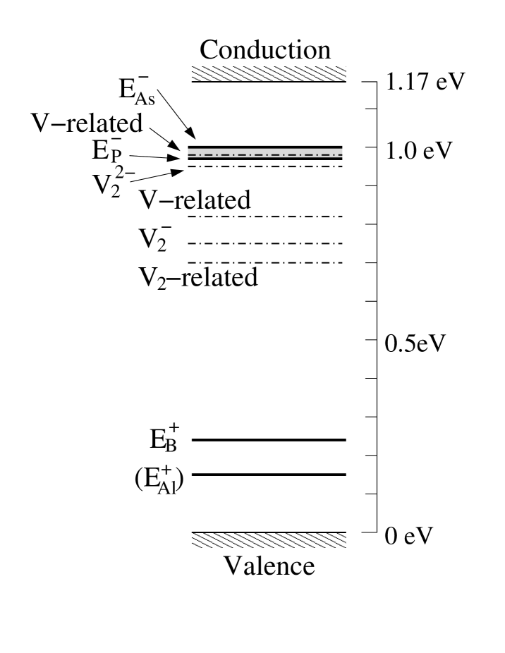
Figure 12 shows the energy levels of the defect responsible for the SPE process according to the GFLS model using a fixed degeneracy value expected of a dangling bond-type defect (0.5 and 1 for the negative and positive defect, respectively). The area between the and is shaded to indicate that we do not expect these levels to be different and therefore may lie somewhere in this range. To provide some reference point for these energy levels with respect to known defect levels in -Si the energy levels of some vacancy-related defects are also shown. These energy levels were measured in -type silicon using deep-level transient spectroscopy and their associated energy levels are: V-related ( eV),Palmetshofer and Reisinger (1992) V-related ( eV), V ( eV), V ( eV) and V2-related ( eV).Huppi (1990) The two vacancy related defects giving energy levels at eV and eV are very close to the levels of the negatively charged defect predicted by the GFLS model. Vacancy related defect levels are included here just to show that values for are consistent with band gap positions of some known defects. We do not know of the existence of any energy level values for DBs in -Si in the literature. Recently, McCallum mentioned that the GFLS model could be extended to predict the energy level of the SPE defect at the - interface by accounting for band bending between the amorphous and crystalline phases.McCallum (1999) A - interface band structure has been proposed by Williams and Elliman which is similar to a junction with the Fermi level on one side of the interface taking the -Si value.Williams and Elliman (1983) In intrinsic material the Fermi level on both the crystalline and amorphous side of the interface are close to mid-gap. When doped the Fermi level on the -Si side will shift in order to satisfy charge neutrality. In -Si, it will generally remain pinned to mid-gap due to the high density of localized states in the center of the band gap. The band structure at the position of the SPE defect residing at the interface can be varied with a weighting function of the form
| (4) |
where is the weighting factor and is the Fermi level of -Si. A value of would result in the Fermi level at the interface being equal to the bulk crystalline value. This is equivalent to the original GFLS model. A value of would result in the value at the interface being shared by the crystalline and amorphous phases. Finally, with a value of , the Fermi level is pinned to mid-gap in the amorphous phase and doping may have little effect.
Details of the band structure of -Si are relatively sparse and lacking in consistency. For hydrogen-free as-implanted intrinsic -Si Stolk et al. have determined the value of the band gap at room temperature to be eV.Stolk and Saris (1994) An empirical formula for thermal BGN in hydrogenated -Si has been reported by Bube et al.Bube et al. (1994) They estimate a decrease of about 50 meV in the band gap between temperatures of 300 and 400 K. Likewise, Premachandran et al. have reported the temperature dependence of the mobility edge of -Si to be eV/K and that both and contribute equally to the narrowing.Premachandran et al. (1984) The Fermi level shift was also found to be eV/K. There is also some evidence that the effective mass is larger in -Si than it is in -Si which would affect the effective DOS values.Chen et al. (1994) Data on doping effects in H-free -Si in the concentration range relevant to SPE are extremely sparse. In short, a complete and reliable picture of the amorphous band structure is lacking from the literature. Once known, the inclusion of Eq. 4 into the GFLS model calculations would be straight forward and may provide a more complete picture of the SPE process.
Figure 13a) shows a possible band structure diagram at the - interface for -type Si. The Fermi level remains constant across the interface region causing band bending to occur. The weighting factor scale is indicated above this band bending. The SPE defect level is placed at . Fig. 13b) shows the possible band structure of the same material if the Fermi level were to come unpinned on the amorphous side of the interface through the filling of mid-gap states as found for high dopant concentrations (1 at.%) by Coffa and co-workers.Coffa et al. (1993); Coffa and Poate (1993) H is also known to passivate defects in -Si and could also modify the band bending at the interface. In fact, the Fermi level has been shown to have a linear dependence on the defect density in -Si:H which can be controlled by the H concentration or the substrate temperature, at least in deposited -Si:H films.Bube et al. (1994) If the SPE defect resides within the band bending region and unpinning occurs the Fermi level shifts closer to this level. Consequently, the SPE defect population increases causing a further enhancement of the SPE rate. This suggests that the dopant concentration would be ‘effectively’ underestimated and that this underestimation increases with dopant concentration or as band bending becomes less pronounced. This may explain the concentration dependence of the SPE defect level, , in Fig. 11 that was found through fitting our SPE data.
V Conclusion
Dopant-enhanced SPE has been measured for buried -Si layers doped with P, B or Al over the concentration range and compared to As-enhanced SPE data published by McCallum in Ref. McCallum (1999). The GFLS model was extended by seeking the best values for temperature and concentration dependences of the parameters involved. A theoretical calculation of the Fermi level for extrinsic and degenerately doped Si fully justified the use of degenerate semiconductor statistics in the concentration and temperature range considered. Although there are relatively large differences in values predicted using various parameterisations we found that these only contribute a 3% error in values. Values of the energy level and the degeneracy of the defect level responsible for SPE obtained from our fits were: As(, ), P(, ), B(, ) and Al(, ). Apart from the Al data which showed anomalous SPE regrowth behaviour these values are remarkably similar to what one might expect for a DB type defect despite the complexity of the fitting procedure.
The GFLS model was extended to consider band bending at the - interface but the lack of a complete description of -Si prevented the extraction of any useful data at this time. However, it was reasoned that band bending could explain the concentration dependence of the defect level that was observed.
The calculation of the Fermi level in -Si for SPE studies could be made more self-consistent if the various parameterisations in the literature are avoided in favour of Monte-Carlo simulations from first principles. Advanced device simulations are often performed with the aid of programs such as TCAD.tca (www.ise.com) This work would also benefit from a similar calculation of the - interface growth process in order to link the band gap states reported in this paper with particular defects. Designing an independent experiment to support the results is difficult. However, the high quality of the data and fits and the extensive parameter review presented here should serve as a good starting point for such calculations.
Acknowledgements.
The Department of Electronic Materials Engineering at the Australian National University is acknowledged for their support by providing access to SIMS and ion implanting facilities.*
Appendix A
A.1 Fermi Level Equations
The carrier concentrations in the conduction and valence bands in an intrinsic semiconductor are commonly given bySze (1976)
| (5a) | |||
| and | |||
| (5b) | |||
where and are the effective DOS in the conduction and valence bands, respectively. For an intrinsic semiconductor these concentrations are equal so these equations can be solved for the Fermi level in intrinsic Si, given that energy levels of the conduction and valence band edges, and , and the associated effective DOS are known.
Likewise, Eq.5 can be solved for the Fermi level for an extrinsic semiconductor. For an -type semiconductor, if the donor concentration, is large compared to the intrinsic carrier concentration, then it is a reasonable approximation to set the carrier concentration, equal to the ionized donor concentration.
However, for highly doped semiconductors Eq. 5a is no longer valid as the expressions for the carrier concentrations are based on classical approximations to the Fermi distribution. These approximations deviate significantly from the Fermi distribution once the Fermi level lies within 3 of the band edges. In this regime degenerate semiconductor statistics must be used. Thus, Eq. 5a becomes
| (6) |
where is the Fermi-Dirac integral. The most accurate approximation to this intractable integral is the Bednarczyk approximation with an error of less than .Bednarczyk and Bednarczyk (1978) We can use this approximation to numerically solve the charge neutrality condition,
| (7) |
For an -type semiconductor we assume that . The concentration of charged donor ions, , is given by the Fermi-Dirac weighting function,
| (8) |
where is the energy level that the charged donor ions introduce into the band gap. According to Sze and Irvin has values of , and meV for As and P and acceptor energy levels of and meV for B and Al, respectively.Sze and Irvin (1968) The degeneracy factor, is equal to 2 for donor levels and 4 for acceptor levels.Sze (1976) In the analysis that follows we assume that every implanted dopant atom is electrically active and hence has the opportunity to become ionized. However, it has been reported that a saturation of the SPE regrowth rate is reached when the dopant concentrations of As, P or B exceed their respective solid solubility limits.Olson and Roth (1988) In this high concentration regime a fraction of the implanted ions do not become electrically active. For the dopants analysed in our study this limit generally represents the upper boundary of concentrations examined.
The concentration of holes in an -type semiconductor can be determined with Boltzmann statistics as per Eq. 5b since the Fermi level is far from the valence band edge. Eq. 7 for an -type semiconductor then becomes
| (9) |
The Fermi level of a degenerately doped semiconductor can then be solved numerically and substituted into Eq.3 if , and their temperature and dopant concentration dependences are known. An outline of the parameters used in this calculation is presented in the next section.
A.2 Si band structure
There are three main sets of parameters that can be used to construct a picture of the band gap structure. These are: expressions outlined by Sze, commonly referred to as the model;Sze (1976) numerical relations compiled by Green;Green (1990) and Monte Carlo simulations. Smith et al. (1999). It is well known that the model is inaccurate even in the device operation temperature regime. Green’s relations are valid only up to 500 K. However, these relations are often extrapolated for use in device simulations in the processing temperature regime given that measurements performed at elevated temperatures are lacking in the literature. Monte Carlo simulations do offer consistent and physical models but require sophisticated simulation software.
This section reviews our current understanding of the parameters used to describe the band structure of Si. It also aims to select a consistent and reliable parameter set for intrinsic and doped -Si between 460 and 660oC so that the expressions for the Fermi levels presented above can be calculated. Monte Carlo simulations are not considered at this time.
A.2.1 Band Gap Narrowing
The band gap width has a temperature dependence arising from the dilation of the lattice. At elevated temperatures, electron-phonon interactions also become important. Theory predicts that thermal band gap narrowing (BGN) should be linear at high temperatures and non-linear at low temperatures. This behaviour is well described by the semi-empirical formula given by Varshni,Varshni (1967)
| (10) |
where is the energy gap at K. It is usually assumed that this variation is distributed evenly between the conduction and valence bands so that each is shifted by an amount towards mid-gap. and are fitting parameters which have taken on a number of different values in the past depending on the availability of data. Recently, Alex et al. have performed photoluminescence experiments and determined the BGN in the temperature range 2 - 750 K.Alex et al. (1996) They have found and K with eV. Smith et al. have used these parameters to model transition metal defect behaviour between 1100 and 1400 K.Smith et al. (1999)
The band gap is also known to be reduced upon heavy doping (for a review see Ref. Jain et al. (1991)). The concentration dependence of BGN arises through the interaction of carriers created thermally with carriers introduced by the dopant and the dopant ion itself.Lindefelt (1998) An exact description of this narrowing has been controversial because optical and electrical measurements give different results with the latter yielding considerably higher BGN values. Klaassen has presented a unified apparent BGN function.Klaassen et al. (1992) This formulation has brought together the disparate data from optical and electrical measurements by correcting the transport equations used in models to interpret electrical data with new accurate values of the intrinsic carrier concentration reported by Green.Green (1990) This formulation also agrees fairly well for dopant concentrations between and to a recent theoretical model proposed by Schenk based on quantum mechanical principles using a full random phase approximation.Schenk (1998)
A.2.2 Effective DOS and the Intrinsic Carrier Concentration
The effective DOS is used to calculate the concentration of carriers in the conduction and valence bands in Eq. 5. Often, the effective DOS is calculated assuming that the bands are parabolic resulting in the model given by SzeSze (1976)
where is the number of equivalent minima in the conduction band and and are the effective electron and hole masses, respectively. To our knowledge there is no experimental data for the effective mass or the effective DOS in the processing temperature regime of interest in our SPE measurements. Therefore, an extrapolation of fits to data collected at lower temperatures is unavoidable.
The electron effective mass used by Green to calculate the effective DOS is valid up to a temperature of 300 K and was found to depend on the band gap width.Green (1990) Green’s electron effective mass values compare well with results by Hensel et al. at a temperature of 4.2 K.Hensel et al. (1965) Green’s values at room temperature are lower than the commonly used values of Barber.Barber (1967) However, the expected weak temperature dependence ensured that values would be accurate to within a few percent up to a temperature of 500 K.
The hole effective mass reported by Green is much greater than that reported by Barber and for temperatures above 230 K Green’s relations suggest that the hole effective mass becomes greater than the electron effective mass. However, this is justified by more recent and rigorous calculations performed by Humphreys,Humphreys (1981) Madarasz et al.,Madarasz et al. (1981) and indium ionisation data by ParkerParker (1983) for temperatures up to 500 K.
The intrinsic carrier concentration has been determined experimentally by Morin and Maita for temperatures between 10 and 1100 K.Morin and Maita (1954) We can therefore look for a consistent set of parameters that follow the trend in the Morin and Maita data by considering the law of mass action which relates the effective DOS and the intrinsic carrier concentration, :
| (12) |
Figure 14 shows the variation of the intrinsic carrier concentration according to several authors as a function of temperature over the range of our SPE data. The intrinsic carrier concentration by Morin and Maita is shown as a solid line. If we assume that the effective mass has no temperature dependence and that the effective DOS has only a dependence then we obtain the solitary curve (dot-dot-dash curve) in Fig. 14.
We have chosen to use the Varshni equation (Eq. 10) with parameters reported by AlexAlex et al. (1996) and the effective electron mass reported by Green et al..Green (1990); Lang et al. (1983) This results in a 3% variation relative to the Morin and Maita data.
Furthermore, we have also chosen to ignore the concentration dependence of the effective mass. The DOS of the conduction band edge is large in Si and the non-parabolicity is small so a change in effective mass is expected to only occur for extremely high fluences. Generally, the free carrier effective mass may increase significantly for concentrations in excess of .Miyao et al. (1981); Slaoui and Siffert (1985) However, no empirical formulations of the concentration dependence exists in the literature and the highest concentration used in the experiments reported in this paper is .
A.3 Fermi Level Calculations
Figure 15 shows the concentration at which degenerate semiconductor statistics become important. Here the Fermi level was calculated as a function of the dopant concentration using Eq. A.1 at a temperature of 460oC. This is the lowest temperature used in these experiments and, for a constant concentration, the Fermi level will be closest to the band edge at this temperature. Above a dopant concentration of the Fermi level crosses over the 3 window and into the degenerate regime. This is true for both As and P donor impurities as their defect levels lie relatively close together and are expected to have a similar effect on the Fermi level position.
Fig. 15 also shows the Fermi level of an extrinsic semiconductor calculated using Eq. 5. Both Fermi levels agree within a dopant concentration range of about . In the lower concentration range () the approximation that is no longer appropriate as carriers generated thermally will dominate the electrical properties of the semiconductor. In the high concentration regime () the classical distribution function cannot be used.
For a -type semiconductor the concentration at which the Fermi level crosses the 3 window will be different. This is mainly a result of the valence band effective DOS being about 40% greater than the conduction band effective DOS as calculated with Green’s relations. Therefore, we might expect the dopants to have less effect on the Fermi level position. Using the same method as above the concentration at which a boron doped semiconductor becomes degenerate is . For Al, having a deeper ionization level in the band gap, the concentration is .
Dopant concentrations at which dopant-enhanced SPE is observable are generally above so using a degenerate approach to calculate the Fermi level is totally justified for all dopant-enhanced SPE studies.
References
- Lu et al. (1990) G. Q. Lu, E. Nygren, M. J. Aziz, and D. Turnbull, Appl. Phys. Lett. 56, 137 (1990).
- Lu et al. (1991) G. Q. Lu, E. Nygren, and M. J. Aziz, J. Appl. Phys. 70, 5323 (1991).
- Csepregi et al. (1978) L. Csepregi, E. F. Kennedy, J. W. Mayer, and T. W. Sigmon, J. Appl. Phys. 49, 3906 (1978).
- Csepregi et al. (1977a) L. Csepregi, E. F. Kennedy, T. J. Gallagher, J. W. Mayer, and T. W. Sigmon, J. Appl. Phys. 48, 4234 (1977a).
- Roth et al. (1990) J. A. Roth, G. L. Olson, D. C. Jacobson, and J. M. Poate, Appl. Phys. Lett. 57, 1340 (1990).
- Suni et al. (1982a) I. Suni, G. Goltz, M. G. Grimaldi, and M.-A. Nicolet, Appl. Phys. Lett. 40, 269 (1982a).
- Williams and Elliman (1983) J. S. Williams and R. G. Elliman, Phys. Rev. Lett. 51, 1069 (1983).
- Lietoila et al. (1982) A. Lietoila, A. Wakita, T. W. Sigmon, and J. F. Gibbons, J. Appl. Phys. 53, 4399 (1982).
- Mosley and Paesler (1985) L. E. Mosley and M. A. Paesler, J. Appl. Phys. 57, 2328 (1985).
- Walser and Jeon (1992) R. M. Walser and Y.-J. Jeon, Mat. Res. Soc. Symp. Proc. 205, 27 (1992).
- Park et al. (1988) W. W. Park, M. F. Becker, and R. M. Walser, Appl. Phys. Lett. 52, 1517 (1988).
- Johnson and McCallum (2004) B. C. Johnson and J. C. McCallum, J. Appl. Phys. 95, 4427 (2004).
- McCallum (1996) J. C. McCallum, Appl. Phys. Lett. 69, 925 (1996).
- McCallum (1999) J. C. McCallum, Nucl. Inst. Meth. B 148, 350 (1999).
- Suni et al. (1982b) I. Suni, G. Goltz, and M.-A. Nicolet, Thin Solid Films 93, 171 (1982b).
- Csepregi et al. (1977b) L. Csepregi, R. P. Kullen, J. W. Mayer, and T. W. Sigmon, Solid State Commun. 21, 1019 (1977b).
- van Vechten and Thurmond (1976) J. van Vechten and L. D. Thurmond, Phys. Rev. B. 14, 3539 (1976).
- Spaepen (1978) F. Spaepen, Acta Metall. 26, 1167 (1978).
- Bourgoin and Germain (1975) J. C. Bourgoin and P. Germain, Phys. Lett. 54A, 444 (1975).
- Bourgoin and Lannoo (1983) J. Bourgoin and M. Lannoo, Point defects in semiconductors II (Springer, Berlin, 1983).
- Saito and Ohdomari (1981) T. Saito and I. Ohdomari, Philos. Mag. B 43, 673 (1981).
- Saito and Ohdomari (1984) T. Saito and I. Ohdomari, Philos. Mag. B 49, 471 (1984).
- Bernstein et al. (1998) N. Bernstein, M. J. Aziz, and E. Kaxiras, prb 58, 4579 (1998).
- Bernstein et al. (2000) N. Bernstein, M. J. Aziz, and E. Kaxiras, prb 61, 6696 (2000).
- Mattoni and Colombo (2004) A. Mattoni and L. Colombo, prb 69, 045204 (2004).
- Roth and Olson (1994) J. A. Roth and G. L. Olson, Handbook of Crystal Growth 3 (Elsevier, Amsterdam, 1994), 3rd ed.
- pro (.) Implant Sciences Corporation Profile (No. 5, 107 Audubon Road, Wakefield, Massachusetts, USA, 01880-1246, (617) 246-0700, .).
- Huppi (1990) M. W. Huppi, J. Appl. Phys. 68, 2702 (1990).
- Palmetshofer and Reisinger (1992) L. Palmetshofer and J. Reisinger, J. Appl. Phys. 72, 2167 (1992).
- Stolk and Saris (1994) P. A. Stolk and F. W. Saris, J. Appl. Phys. 75, 7266 (1994).
- Bube et al. (1994) R. H. Bube, L. Benatar, and D. Redfield, J. Appl. Phys. 75, 1571 (1994).
- Premachandran et al. (1984) V. Premachandran, K. L. Narasimhan, and D. R. Bapat, Phys. Rev. B. 29, 7073 (1984).
- Chen et al. (1994) K. H. Chen, Y. K. Fang, and K. H. Shieh, Appl. Phys. Lett. 65, 2815 (1994).
- Coffa et al. (1993) S. Coffa, F. Priolo, J. M. Poate, and S. H. Glarum, Nucl. Inst. Meth. B 80/81, 603 (1993).
- Coffa and Poate (1993) S. Coffa and J. M. Poate, Appl. Phys. Lett. 63, 1080 (1993).
- tca (www.ise.com) ISE Integrated Systems Engineering G, ISE TCAD software including (DESSIS), Release 4.0 (Zurich, www.ise.com).
- Sze (1976) S. M. Sze, Physics of Semiconductor Devices (John Wiley and Sons, 1976), 2nd ed.
- Bednarczyk and Bednarczyk (1978) D. Bednarczyk and J. Bednarczyk, Phys. Lett. 64A, 409 (1978).
- Sze and Irvin (1968) S. M. Sze and J. C. Irvin, Solid State Electron. 11, 599 (1968).
- Olson and Roth (1988) G. L. Olson and J. A. Roth, Mat. Sci. Rep. 3, 1 (1988).
- Green (1990) M. A. Green, J. Appl. Phys. 67, 2944 (1990).
- Smith et al. (1999) A. L. Smith, S. T. Dunham, and L. C. Kimerling, Physica B 273-274, 358 (1999).
- Varshni (1967) Y. P. Varshni, Physica 34, 149 (1967).
- Alex et al. (1996) V. Alex, S. Finkbeiner, and J. Weber, J. Appl. Phys. 79, 6943 (1996).
- Jain et al. (1991) S. C. Jain, R. P. Mertens, and R. J. V. Overstraeten, Advances in Electronics and Electron Physics (Edited by P. W. Hawkes) Vol 82, 197-275 (Academic Press, London, 1991).
- Lindefelt (1998) U. Lindefelt, J. Appl. Phys. 84, 2628 (1998).
- Klaassen et al. (1992) D. B. M. Klaassen, J. W. Slotboom, and H. C. D. Graaff, Solid State Electron. 35, 125 (1992).
- Schenk (1998) A. Schenk, J. Appl. Phys. 84, 3684 (1998).
- Hensel et al. (1965) J. C. Hensel, H. Hasegawa, and M. Nakayama, Phys. Rev. 138, A225 (1965).
- Barber (1967) H. D. Barber, Solid State Electron. 10, 1039 (1967).
- Humphreys (1981) R. G. Humphreys, J. Phys. C: Solid State Phys. 14, 2935 (1981).
- Madarasz et al. (1981) F. L. Madarasz, J. E. Lang, and P. M. Hemeger, J. Appl. Phys. 52, 4646 (1981).
- Parker (1983) G. J. Parker, J. Appl. Phys. 54, 3926 (1983).
- Morin and Maita (1954) F. J. Morin and J. P. Maita, Phys. Rev. 96, 28 (1954).
- Lang et al. (1983) J. E. Lang, F. L. Madarasz, and P. M. Hemeger, J. Appl. Phys. 54, 3612 (1983).
- Miyao et al. (1981) M. Miyao, T. Motooka, N. Natsuaki, and T. Tokuyama, Solid State Commun. 37, 605 (1981).
- Slaoui and Siffert (1985) A. Slaoui and P. Siffert, Phys. Status Solidi A 89, 617 (1985).