Anomalously large capacitance of a plane capacitor with a two-dimensional electron gas
Abstract
In electronic devices where a two-dimensional electron gas (2DEG) comprises one or both sides of a plane capacitor, the resulting capacitance can be larger than the “geometric capacitance” determined by the physical separation between electrodes. This larger capacitance is known to result from the Coulomb correlations between individual electrons within the low density 2DEG, which lead to a negative thermodynamic density of states. Experiments on such systems generally operate in the regime where the average spacing between electrons in the 2DEG is smaller than , and these experiments observe by only a few percent. A recent experiment Ashoori , however, has observed larger than by almost 40% while operating in the regime . In this paper we argue that at correlations between the electronic charge of opposite electrodes become important. We develop a theory of the capacitance for the full range of . We show that, in the absence of disorder, the capacitance can be times larger than the geometric value, where is the electron Bohr radius. Our results compare favorably with the experiment of Ref. Ashoori, without the use of adjustable parameters.
I Introduction
In a standard parallel-plate capacitor, the capacitance is equal to the “geometric capacitance” (in Gaussian units), where is the dielectric constant of the medium separating the two plates, is the area of each plate, and is the separation between them. The expression is correct when both electrodes are made from a “perfect” metal, which by definition screens electric field with a vanishing screening radius, so that the charge of a given electrode is located exactly on the electrode surface and the electric field from the opposite electrode does not penetrate into the metal. If one of the electrodes is made from a material with finite (positive) Debye screening radius (for example, a doped bulk semiconductor), then the imperfect charge screening at this electrode allows the electric field to penetrate a distance into the electrode and the capacitance decreases. If one describes the capacitance by the effective capacitor thickness , then the effect of positive screening radius is to increase the effective capacitor thickness from to .
On the other hand, capacitors with , or in other words with effective three-dimensional electrode screening radius , are known in semiconductor physics BLES1981 ; Luryi ; KRAV1990 ; Eis1992 ; Eis-long ; Sivan ; Jiang ; Yacoby ; Allison ; SE ; Efros92 ; Pikus92 ; Pikus93 ; Shi ; Fogler ; Efros08 ; Kopp . Examples include Si MOSFETs and gated GaAs-AlGaAs heterostructures, where one electrode consists of a clean, low density, two-dimensional electron gas (2DEG) KRAV1990 ; Eis1992 ; Eis-long ; Sivan ; Jiang ; Yacoby ; Allison . In these devices, the total capacitance can be written as
| (1) |
where is the electron area density, is the chemical potential of the 2DEG, and is the elementary charge. In terms of the effective thickness , Eq. (1), implies
| (2) |
where is the Debye screening radius of the 2DEG. Capacitance larger than the geometric value, or , is possible when the thermodynamic density of states of the 2DEG is negative (or, equivalently, when the compressibility ).
In the limit of low electron density, such that the average distance is much larger than the effective Bohr radius of the electrons, or in other words the dimensionless parameter , a 2DEG is a classical system whose physics is dominated by the Coulomb interaction between electrons. This interaction leads to a Wigner crystal-like strongly-correlated liquid state with negative chemical potential . The corresponding Debye screening radius produces a negative correction BLES1981 ; foot to :
| (3) |
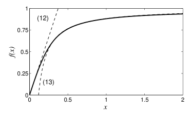
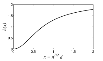
What happens to when ? This is the main question addressed in this paper. Thermodynamic stability criteria ensure that the capacitance cannot be negative LL8 , so Eq. (3) must not apply at such low densities. In Sec. II of this paper we find the function , valid over the whole range of . The dimensionless function is shown in Fig. 3. We show that in the limit the effective thickness becomes very small:
| (4) |
This dramatic capacitance growth is due to the coupling of each electron in the 2DEG to its image charge in the metal electrode. At low density, compact electron-image dipoles are separated from each other by a distance much larger than their dipole arm. These dipoles interact weakly with each other, providing only a small resistance to capacitor charging.
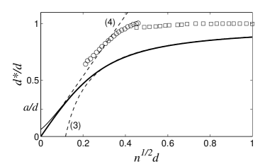
Until recently, only relatively small corrections to the geometrical capacitor thickness were observed experimentally KRAV1990 ; Eis1992 ; Eis-long ; Sivan ; Jiang ; Yacoby ; Allison . The most recent paper on this subject Ashoori , however, claims a much larger correction for a YBa2Cu3O7/LaAlO3/SrTiO3 (YBCO/LAO/STO) capacitor with a 2DEG at the LAO/STO interface separated by nm of LAO insulator from the metallic YBCO gate. Theoretical estimates show that nm is by far the smallest length scale in the problem, so that as a zero-order approximation one can use a classical description of the 2DEG. This measurement calls for a comparison of our function with the experimental data of Ref. Ashoori, . Such a comparison is shown in Fig. 1 and looks quite good without the use of adjustable parameters. We return to a more detailed discussion of this comparison in Sec. IV.
In Sec. III we study the case where both sides of the capacitor are made from 2DEGs with equal electron density . Such a capacitor in principle can be realized in devices with two parallel quantum wells with tunable concentrations of electrons Eis-long , but we do not know of any published results. The capacitance of such devices was addressed theoretically in Ref. Kopp, . In the limit , the authors of Ref. Kopp, arrive at a small correction to which is twice larger than for that of one 2DEG: . In the classical limit , this gives . The authors of Ref. Kopp, assume that this equation remains valid even at , which leads them to the prediction that diverges and becomes negative at a finite value of . As the authors themselves recognized, however, their assumption ignores correlations between the two 2DEGs. In Sec. III we account for these correlations and demonstrate that they dramatically alter the results of Ref. Kopp, for . Namely, vanishes and diverges only in the limit , as in the case of a single 2DEG. The transition from large to small for two 2DEGs is described by the equation , where is the same function as for the single 2DEG case. Also similar to the single 2DEG case, the diverging capacitance can be explained by strong correlations between the Wigner crystals of the two 2DEGS, so that an electron transferred from one 2DEG to the other is still bound to its image charge (the hole left behind in the opposite electrode, see Fig. 5). Thus, at only the weak dipole-dipole repulsion between two electron-hole dipoles is responsible for resistance to charging of the 2DEGs capacitor.
Of course, the divergence of the capacitance at takes place only at simultaneously vanishing Bohr radius , temperature, disorder, and, in the case of two 2DEGs, probability of tunneling through the insulator. At some strength these factors destroy the Coulomb correlations between electrons at a particular value of and truncate the capacitance growth, so that at the capacitance remains finite. Such a behavior is shown schematically by the thin line in Fig. 1, which assumes vanishing temperature and disorder but finite . We see that the capacitance can grow as much as 16 times from the geometrical value.
Usually, disorder is so severe that it closes the window of in which is substantially smaller than . Nonetheless, the experiment of Ref. Ashoori, shows a large correction, so that apparently such a window is open. In Sec. IV we discuss this experiment in greater detail in an attempt to understand why it represents a special case where large capacitance can be observed. We also discuss the effects of the quantum kinetic energy of electrons in the 2DEG, and show that in the absence of disorder it provides an upper limit for the capacitance at .
We note that this paper represents an extension of an approach we have previously used to study large capacitance at the interface between a metal and an ionic conductor (an ion-conducting glass us-PRL ; us-longer or an ionic liquid Loth ). Such interfaces block both ionic and electronic current, thereby forming a capacitor even in the absence of an insulating layer. The binding of discrete ions to their image charges in the metal results in a weaker, dipole-dipole repulsion between counterions and therefore in large capacitance of the interface. The resulting effective thickness of the capacitor can, surprisingly, be even smaller than the ion radius. This paper describes a similar effect for systems where the countercharge consists of a 2DEG separated from the metal by an insulator. Over a certain range of the electron density , the capacitance in such systems is dominated by the strong Coulomb interactions between discrete charges and can therefore be described using a classical analysis similar to that of Refs. Loth, ; us-PRL, ; us-longer, . A very brief report about the first part of this work was published in our recent preprint Loth .
Our general approach to calculating the capacitance in the sections below is as follows. We first describe the total electrostatic energy associated with the ground state configuration of electrons per unit area. If the two sides of the capacitor are coupled through a voltage source with voltage , then the value of the charge of the capacitor is that which minimizes the total energy , where the term represents the work done by the voltage source relative to the situation . Using the (zero-temperature) equilibrium condition along with gives
| (5) |
The differential capacitance (or “charge susceptibility”) of the system can therefore be written
| (6) |
We can solve for the capacitance as a function of voltage, , by combining this relation with Eq. (5). Finally, the effective capacitor thickness is also defined by the total energy as
| (7) |
In this way a description of the total energy is sufficient to determine the capacitance, and it is not necessary to invoke the Poisson equation or to make mean-field approximations of the electric potential.
II Capacitor with a classical 2DEG and a metal electrodes
In this section we describe a 2DEG with area density separated from a perfect metal electrode by an insulator of thickness . This can be, for example, a Si MOSFET or a gated GaAs-AlGaAs heterostructure, where a 2DEG is created at the semiconductor-insulator interface and connected to one terminal of a voltage source by ohmic contacts. The metal electrode is connected to the opposite terminal of the voltage source. For simplicity, we assume that the dielectric constant is uniform everywhere. We treat the 2DEG in the classical limit .
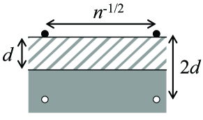
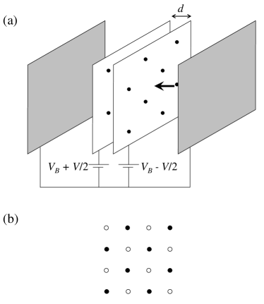
In the ground state for low electron density , the repulsion between electrons within the 2DEG causes them to form a strongly-correlated liquid, reminiscent of a two-dimensional Wigner crystal, in which electrons are separated from their nearest neighbors by a distance . Each electron, of charge , also induces an image charge, , in the metal surface, which is effectively located a distance from the 2DEG. This situation is shown schematically in Fig. 2. We suppose that the 2DEG is connected to some voltage source which maintains a difference in electric potential between the 2DEG and the metal electrode. The charge of the capacitor is defined as the amount of charge that has moved through the voltage source relative to the state .
A given electron within the 2DEG and its image charge effectively form an electron-image dipole, with dipole moment , which repels an adjacent electron. In the limit , we can use the point-dipole approximation and the repulsive energy between two adjacent electrons is . More generally, we can write the total electrostatic energy of the electrons in the 2DEG by first calculating the electrostatic potential experienced by each electron relative to infinity. Specifically, for an electron located at the origin
| (8) |
where the indices label the set of electron locations and is the distance between the electron and the origin. The term outside the sum in Eq. (8) indicates the potential contributed by the electron’s own image charge, which is added in place of the self-interaction term . can be estimated by assuming that the electrons occupy a regular square lattice with lattice constant , in which case
| (9) |
where is a dimensionless function
| (10) |
The sum in Eq. (10) is convergent for all . We note that while the true lowest energy configuration for the electrons is to occupy a triangular lattice, the energy per unit area of a square lattice of dipoles differs from that of a triangular lattice by less than Topping , so for computational simplicity we use a square lattice for all calculations.
The total energy of the configuration of electrons is
| (11) |
Combining Eqs. (11) and (7) gives
| (12) |
where .
The dimensionless function is plotted in Fig. 3. At , one can expand the summand in Eq. (10) to lowest order in and arrive at the point-dipole approximation for the interaction among electron-image pairs, which after summation gives . The resulting effective capacitor thickness approaches zero linearly with , and the function is described by
| (13) |
which is equivalent to Eq. (4). This vanishing of at implies that the capacitance diverges when the electron gas is very sparse. Such diverging capacitance is the result of a vanishing dipole-dipole repulsion between adjacent electron-image pairs as the electron density goes to zero.
At large electron density , the effective thickness approaches the geometric thickness . In other words, approaches . In the region , the difference between and can be viewed as a small correction associated with a finite negative screening radius of the 2DEG. In this case approaches
| (14) |
which is equivalent to Eq. (3). It is only at much larger density , that quantum effects cause the 2DEG screening radius to become positive, so that becomes larger than .
We can also derive a relation between the voltage of the capacitor and the electron density by using Eq. (5). If we define to be the “threshold voltage” at which the electron gas is completely depleted (), then the derivative of Eq. (11) implies that
| (15) |
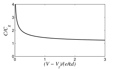
Combining the results of Eqs. (12) and (15) allows us to create a plot of the capacitance as a function of . The result is shown in Fig. 4, with the capacitance and voltage plotted in the dimensionless forms and , respectively. At small voltages , the capacitance diverges as . At large voltages , the capacitance approaches its geometric value.
III Capacitor made from two 2DEGs
One can also imagine a capacitor where 2DEGs comprise both electrodes, as was treated theoretically in Ref. Kopp, . Such a situation is possible in devices with two parallel quantum wells with tunable concentrations and separate contacts. This can be, for example, a GaAs-AlGaAs-GaAs heterostructure, where 2DEGs are formed at both heterojunctions. The densities of the two 2DEGs can be tuned by applying a large bias voltage above each of them. If a small additional voltage is applied between the two 2DEGs, then the response to this small voltage can be used to determine the capacitance of the two-2DEG system. This setup is shown schematically in Fig. 5(a).
In this section we consider the case of two identical 2DEGs oriented parallel to each other and separated by a distance . They are connected to opposite terminals of a voltage source maintained at a particular voltage . We assume that at both 2DEGs have the same density of electrons and that charge neutrality is maintained by a uniform plane of surface charge with density that coincides with the plane of each 2DEG. We also assume, for simplicity, that the dielectric constant is uniform everywhere.
At zero temperature, the electron positions are strongly correlated, with electrons in a 2DEG seeking to maximize their separation both from each other and from electrons in the opposite plane. As a result, at electrons form interlocking lattices of electron positions on the two electrodes, as shown schematically in Fig. 5(b). The exact configuration of the two lattices can take on one of three arrangements, depending on the value of the parameter Goldoni . However, the energy of these different lattice types differs by only a few percent, so for illustrative purposes we have shown the simplest case of two interlocking square lattices.
In order to give the two-2DEG capacitor a finite charge , some number of electrons must be transferred from one 2DEG to the other. For one electron, this process requires a finite amount of energy , associated with creating a defect in the two lattices. While a careful calculation of is not a major goal of this paper, we make an estimate of its value at the end of this section.
When the voltage applied between the two 2DEGs is smaller than , no charge transfer is possible and the capacitance . At , some finite area density of electrons is transferred from one 2DEG to the other and the corresponding capacitor charge is . These “excess electrons” also repel each other, and they seek to maximize their distance from each other by forming a Wigner crystal-like lattice of defects in the ground state “checkerboard” of electrons. At low temperature, excess electrons remain coupled to the “holes” they leave behind in the opposite 2DEG and therefore they repel each other by a dipole-dipole repulsion. The form of this repulsion is identical to that of the previous section, where the image charge was formed in the metal electrode, except that in the present case the dipole arm is rather than and there is an overall factor associated with the presence of a repulsive force at both positive and negative sides of the dipole. This similarity allows us to use previous results in writing the total electrostatic energy of the system relative to the ground state. Namely,
| (16) |
where is the same function defined in Eq. (10).
The density of excess electrons can be related to the voltage by . If we define , then this relation gives
| (17) |
As in Eq. (7), the corresponding effective thickness is , which gives
| (18) |
where , plotted in Fig. 3, is the same function as in Eq. (12).
Eq. (18) is correct when the applied voltage is low enough in absolute value that neither 2DEG is depleted. At some critical voltage , however, no additional charge transfer is possible between the two 2DEGs and the capacitance collapses. The value of can be estimated by setting , which corresponds to substituting for in Eq. (17).
We now comment on the threshold energy required to transfer a single electron from one 2DEG to the other at zero voltage. A rough estimate of can be made by imagining that an electron is transferred to the site directly across from it in the opposite 2DEG and that all other electrons remain in their ground state positions. In this case can be evaluated as
| (19) |
where is a dimensionless function
| (20) |
Here, for simplicity, we have again assumed a square lattice of electron positions, as in Fig. 5. The function , which is convergent for all , is plotted in Fig. 6. The estimate of Eqs. (19) and (20) assumes that the lattice of electron positions is undisturbed by the transfer of one electron, which is valid when the 2DEGs are relatively sparse, , which is the major focus of this paper. At larger the lattice is more easily deformed and Eq. (19) represents an upper bound for .
IV Discussion
In this section we discuss the truncation of the capacitance divergence of a classical 2DEG, concentrating primarily on the case of a single 2DEG parallel to a metal electrode. So far we have dealt only with a clean, classical 2DEG. Of course, at zero temperature and in the absence of disorder the capacitance cannot diverge without bound in the limit because of the effects of quantum kinetic energy. This conclusion can be reached by considering that each electron within the 2DEG sits in a potential well created by neighboring electron-image dipoles. If this potential is expanded to second order in the electron’s displacement from the potential well minimum, then we get , where is a numerical coefficient and is the electrostatic potential described by Eq. (9). This potential is that of a two-dimensional harmonic oscillator, and therefore it has a ground state energy , where is defined so that . When , the 2DEG retains its strongly-correlated, Wigner crystal-like structure and the contribution of the quantum kinetic energy to the capacitance is small. At , however, the quantum kinetic energy becomes larger than and the 2DEG loses its electrostatic correlations. This point corresponds to . At vanishingly small values of , the energy of the 2DEG is that of a noninteracting fermion gas, which produces . For the experiments of Ref. Ashoori, , nm and nm, so that apparently in this system a capacitance is possible (see Fig. 1).
The analysis above has also ignored disorder, which can truncate the divergence of the capacitance by destroying dipole-dipole correlations. The presence of disorder modulates the density of the correlated dipole liquid with some characteristic amplitude . At small enough average density , the overall electron density becomes smaller than . This means that screening becomes nonlinear SE and multiple pores open in the 2DEG. Electric field lines starting at the metal gate electrode leak through these pores. As a result, the Debye screening radius changes its sign Eis1992 ; Eis-long ; Sivan ; Jiang ; Yacoby ; Allison ; SE ; Efros92 ; Pikus92 ; Pikus93 ; Shi ; Fogler from negative to positive at some . At smaller the effective thickness grows sharply. In a 2DEG with moderate mobility and large distance to the gate, and the minimum of is very shallow. For example, for the classical 2D hole gas (with large ) in GaAs/GaAlAs heterojunctions studied in Ref. Allison , , while as we see in Fig. 3 the crossover between the and asymptotic dependencies happens only around or .
Larger deviations from the geometrical capacitance can be observed in the cleanest p-GaAs/GaAlAs heterojunction-insulated-gate field-effect transistors (HIGFETs) Huang . In such devices a 2D hole gas is created with concentration as small as cm-2 by a metallic gate at a distance from the 2D gas which can be as small as nm. This gives , so that if disorder permits can be reached. There is no published data on capacitance for this case, but there are indications that screening of the Coulomb interaction between 2D holes by the gate (hole images) plays an important role for transport properties Huang .
One may be able to reach even larger for the capacitance between two 2DEGs residing in two parallel quantum wells, because in this case can be as small as nm Eis1992 ; Eis-long so that already at cm-2. We are not aware of any such measurements.
Another system which may provide a good opportunity for studying capacitance larger than is that of a very low density 2DEG which floats on the top of a thin liquid helium film covering a metallic electrode Grimes ; Konstantinov .
Let us now turn to the most spectacular data, obtained from a YBCO/LAO/STO capacitor Ashoori . We see from Fig. 1 that in this case a much smaller value has been reached than in other cases, resulting in the record for larger-than-geometrical capacitance . This became possible because of the very small distance between the 2DEG and the gate nm. Even at relatively large concentration cm-2, such small thickness leads to . In Fig. 1 the agreement of our theory (which has no adjustable parameters) with the experimental data of Ref. Ashoori looks so good that disorder apparently plays a minor role. The relatively large concentration of electrons may result in a significant resistance to disorder, but the relative unimportance of disorder is nonetheless difficult to understand. No independent estimates of disorder effects in YBCO/LAO/STO capacitor are currently available in literature.
Our comparison with the data of Ref. Ashoori assumes that the 2DEG is localized within a very narrow layer of STO, on the order of one lattice constant, as was shown in Refs. Sing ; Zhong . There are arguments that the electron layer is actually much wider Siemons ; Copie , but these are based on calculations of the nonlinear screening radius of STO using its huge low-temperature dielectric constant . We disagree with using the dielectric constant of STO as measured in uniform crystals when describing nonlinear screening. Indeed, the large dielectric constant of STO (as well as that of displacement ferroelectric crystals) has a strong spatial dispersion. Below we discuss the origin of this dispersion following Ref. Bursian .
The large, low-temperature, zero-frequency dielectric constant of STO is related to the anomalously small frequency of the transverse optical mode at . At , the dielectric constant . For finite , the dielectric constant . The soft mode is known to have very strong dispersion, so that at large it returns to the normal optical mode frequency. This dispersion has the form , where and is the lattice constant Bursian . Using such a strongly dispersive dielectric constant for the description of nonlinear screening by electrons in STO self-consistently leads to the conclusion that the nonlinear screening radius, or in other words the width of the 2DEG, is of the order of the lattice constant . (This same dispersion also explains why the large dielectric constant of STO does not lead to strong electron-phonon coupling and a large increase of the critical temperature of superconductivity Meevasana .)
V Conclusion
In this paper we have shown that in devices where a 2DEG comprises one or both electrodes of a plane capacitor the correlations between electronic charge in opposite electrodes dramatically affect the capacitance at low electron density . In the absence of disorder, this leads to a capacitance that grows strongly with decreasing , with a maximum value corresponding to at . We have presented a prediction for the effective capacitor thickness which is valid over the entire range of and which is based on the Coulomb correlations between electrons and their image charges. The cases of a 2DEG parallel to a metal electrode and of two parallel 2DEGs were considered separately. Our results compare favorably to the recent experiments of Ref. Ashoori, , which operate at and report larger than by as much as 40%, without the use of adjustable parameters.
The experiments of Ref. Ashoori, , which use a 2DEG created at the an LAO/STO interface, are consistent with the 2DEG occupying a very thin layer of STO on the order of one lattice constant, so that the 2DEG can indeed be treated as a two-dimensional system up to fairly high electron density. Further studies on such systems with low disorder and small LAO thickness may provide even better insight into the behavior of the capacitance at small . Systems of very clean HIGFETs, parallel quantum wells, and electrons floating on liquid helium may also provide good opportunities for studying larger-than-geometrical capacitance.
Acknowledgments.
We are grateful to R. C. Ashoori, A. L. Efros, J. Eisenstein, M. M. Fogler, T. Kopp, L. Li, M. S. Loth, and B. Z. Spivak for helpful discussions. B. S. acknowledges the support of the NSF Graduate Research Fellowship.
References
- (1) Lu Li, C. Richter, S. Paetel, T. Kopp, J. Mannhart, and R. C. Ashoori, arxiv:cond-mat/1006.2847 (2010).
- (2) M.S. Bello, E.I. Levin, B.I. Shklovskii, A.L. Efros, Sov. Phys.-JETP 53, 822 (1981)
- (3) S. Luryi, Appl. Phys. Lett. 52, 501 (1988).
- (4) S. V. Kravchenko, D. A. Rinberg, S. G. Semenchinsky, and V. M. Pudalov, Phys. Rev. B 42, 3741 (1990).
- (5) J. P. Eisenstein, L. N. Pfeiffer, and K. W. West, Phys. Rev. Lett. 68, 674 (1992).
- (6) J. P. Eisenstein, L. N. Pfeiffer, and K. W. West, Phys. Rev. B 50, 1760 (1994).
- (7) S. Shapira, U. Sivan, P. M. Solomon, E. Buchstab, M. Tischler, G. Ben Yoseph, Phys. Rev. Lett. 77, 3181 (1996).
- (8) S. C. Dultz, H. W. Jiang, Phys. Rev. Lett. 84, 4689-4692 (2000).
- (9) S. Ilani, A. Yacoby, D. Mahalu, and H. Shtrikman, Phys. Rev. Lett. 84, 3133 (2000).
- (10) G. D. Allison, E. A. Galaktionov, A. K. Savchenko, S. S. Safonov, M. M. Fogler, M. Y. Simmons, D. A. Ritchie, Phys. Rev. Lett. 96, 216407 (2006).
- (11) B. I. Shklovskii and A. L. Efros, JETP Lett. 44, 669 (1987).
- (12) A. L. Efros, Phys. Rev. B 45, 11354 (1992)
- (13) A. L. Efros, F. G. Pikus, and V. G. Burnett, Solid State Comm. 84, 91 (1992).
- (14) F. G. Pikus and A. L. Efros, Phys. Rev. B 47, 16395 (1993).
- (15) J. Shi, X. C. Xie, Phys. Rev. Lett. 88, 086401 (2002).
- (16) M. M. Fogler, Phys. Rev. B 69, 121409(R) (2004).
- (17) A. L. Efros, Phys. Rev. B, 78, 155130 (2008).
- (18) T. Kopp and J. Mannhart, J. Appl. Phys. 106, 064504 (2009).
- (19) Ref. BLES1981, dealt with the case of a small number of repelling holes in the almost filled Na impurity band of a Si MOSFET. In this case the kinetic energy is frozen and the Coulomb repulsion of holes creates Wigner crystal-like order. For a free electron gas it is known that becomes negative Ceperley at , while classical formulas for energy and chemical potential become accurate only at large enough . In the intermediate range one can use quantum mechanical expressions for the energy of the 2DEG, Luryi ; KRAV1990 ; Eis1992 ; Eis-long ; Sivan ; Jiang ; Yacoby ; Allison ; Efros92 ; Pikus92 ; Pikus93 ; Efros08 ; Kopp . leading to qualitatively similar conclusions.
- (20) L. D. Landau, E. M. Lifshitz, and L. P. Pitaevskiĭ, Electrodynamics of Continuous Media, 2nd ed.; Pergamon Press: Boston, 1996, Ch. 1.
- (21) Brian Skinner, M. S. Loth, and B. I. Shklovskii, Phys. Rev. Lett. 104, 128302 (2010).
- (22) M. S. Loth, Brian Skinner, and B. I. Shklovskii, Phys. Rev. E 82, 016107 (2010).
- (23) M. S. Loth, Brian Skinner, and B. I. Shklovskii, arXiv:1005.3065.
- (24) Jian Huang, D. S. Novikov, D. C. Tsui, L. N. Pfeiffer, and K. W. West, Phys. Rev. B 74, 201302(R), (2006); arXiv:cond-mat/0610320.
- (25) J. Topping, Proc. Roy. Soc. Lond. A 114, 67 (1927).
- (26) G. Goldoni and F. M. Peeters, Phys. Rev. B 53, 4591 (1996).
- (27) C. C. Grimes, G. A. Adams, Phys. Rev. Lett. 42, 795 (1979).
- (28) D. Konstantinov, K. Kono arXiv:1006.0349.
- (29) M. Sing, G. Berner, K. Goß, A. Müller, A. Ruff, A. Wetscherek, S. Thiel, J. Mannhart, S. A. Pauli, C. W. Schneider, P. R. Willmott, M. Gorgoi, F. Schäfers, R. Claessen Phys. Rev. Lett. 102, 176805 (2009).
- (30) Z. Zhong, P. X. Xu, P. J. Kelly, arXiv 1006.5146.
- (31) W. Siemons, M. Huijben, G. Rijnders, D. H. A. Blank, T. H. Geballe, M. R. Beasley, G. Koster, Phys. Rev. B 81, 241308(R)(2010).
- (32) O. Copie, V. Garcia, C. Bodefeld, C. Carretero, M. Bibes, G. Herranz, E. Jacquet, J.-L. Maurice, B. Vinter, S. Fusil, K. Bouzehouane, H. Jaffres, A. Barthelemy, Phys. Rev. Lett. 102, 216804 (2009).
- (33) E. V. Bursian, Ya. G. Girshberg, J. de Physique, Colloque C2, suppl. 4, Tome 33, page C2-69 (1972)
- (34) W. Meevasana, X. J. Zhou, B. Moritz, C-C. Chen, R.H. He, S.-I. Fujimori, D.H. Lu, S.-K. Mo, R.G. Moore, F. Baumberger, T.P. Devereaux, D. van der Marel, N. Nagaosa, J. Zaanen, Z.-X. Shen, New Journal of Physics 12 (2010) 023004
- (35) D. Ceperley, Phys. Rev. B 18, 3126 (1978).