Rectification in three-terminal graphene junctions
Abstract
Nonlinear electrical properties of graphene-based three-terminal nanojunctions are presented. Intrinsic rectification of voltage is observed up to room temperature. The sign and the efficiency of the rectification can be tuned by a gate. Changing the charge carrier type from holes to electrons results in a change of the rectification sign. At a bias mV and at a temperature below 4.2 K the sign and the efficiency of the rectification are governed by universal conductance fluctuations.
Graphene has attracted a lot of attention due to its unique properties and a wide field of possible applications. One class of graphene-based devices which has a realistic chance to reach the market is ballistic switches and rectifiers that can operate at ultrahigh-frequencies geim2009 . The main idea of such devices is that the charge carriers move without scattering through the active area of the device or are scattered only by the designed geometry. Typical examples of such nanodevices are three-terminal ballistic junctions (TBJs) xu2001 ; worschech2001 ; shorubalko2001 ; jordan2008 , ballistic rectifiers song1998 ; song2001 , and artificial nanomaterials song2001b . Three-terminal nanojunctions exhibit robust nonlinear rectifying behavior in different material systems: III-V semiconductor heterostructures worschech2001 ; shorubalko2001 ; shorubalko2003 , InAs nanowires suyatin2008 and in carbon nanotubes papadopoulos2000 . A number of devices have been demonstrated based on nonlinear electrical properties of TBJs: frequency multiplier shorubalko2002 , logic gates xu2004 ; muller2007 , set-reset latch device sun2008 , half and full adders reitzensein2004 ; lau2006 . The operation speed of such devices is predicted to be in the THz range mateos2003 .
Ballistic switches and rectifiers in graphene represent another fascinating possibility to realize high quality electronic nanostructures. High charge carrier mobilities are promising for graphene-based ballistic electronics bolotin2008 and the possibility to electrically or environmentally tune graphene from p- to n-type and vice versa schedin2007 gives the opportunity to design adaptive electronic devices yu2009 . Although theoretical proposals have been made for building blocks for integrated graphene circuits areshikin2007 , to the best of our knowledge none of the nanodevices mentioned above has been realized in graphene yet.
Here we set out to realize three-terminal nanojunctions in graphene and investigate their nonlinear electrical properties. Intrinsic rectification of voltage with a switchable sign is observed up to room temperature. The possible mechanisms of rectification and limitations of its efficiency are discussed.
The samples are fabricated by mechanical exfoliation of natural graphite powder followed by the deposition onto a highly doped silicon substrate covered by 285 nm of silicon dioxide novoselov2004 . The doped silicon substrate is used as a global backgate to change the overall Fermi energy of the device. Single layer flakes are identified by optical microscopy and Raman spectroscopy ferrari2006 ; graf2007 . The Ohmic contacts are defined by electron beam lithography followed by the evaporation of Cr/Au (2 nm/40 nm), and the structure is patterend in a second electron beam lithography step followed by reactive ion etching.
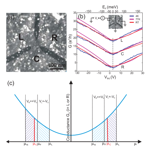
In Fig. 1(a) a scanning force micrograph (SFM) of the center part of the device is depicted. The leads, labeled L (left), R (right) and C (center) are separated by three constrictions which are 200 nm wide. The angle between each branch of the junction is approximately 120 degrees which makes the device rotationally symmetric and it can be measured in three comparable configurations in the non-linear transport regime (see measurement configuration below). To characterize the junction the conductance () of each constriction is measured as a function of the applied backgate voltage () at 4 K, 77 K and room temperature in the linear response regime as shown in Fig. 1(b) (The electrical measurement configuration can be seen in the inset). The Fermi energy calculated from the backgate voltage by assuming a density of states linear in energy is plotted as the upper horizontal axis. The point of minimum conductance, the Dirac point, is located at approximately +3V in backgate (see the dashed line in Fig. 1(b)) and we set the Fermi energy to be zero at this point. To the left of the Dirac point the charge carriers are holes and to the right we have electron transport. Thus, by changing we can tune the device from p-type to n-type. At 4 K reproducible universal conductance fluctuations (UCFs) are visible. At 77 K and room temperature the UCFs are smeared out and the conductance curves are smooth. The conductance of each of the constrictions is similar suggesting that the device is close to symmetric. From the conductance curves we estimate the mobility of the junction to be cm2/Vs and the corresponding mean free path to be nm. Thus, the device can be considered to be diffusive.
In previous measurements and calculations it has been shown that for a symmetric III-V-based three-terminal ballistic junction in the non-linear regime the voltage on the center branch () is always negative when the bias voltages at the left and the right branches are applied in a push-pull fashion with shorubalko2001 ; worschech2001 ; xu2001 . For a graphene three terminal junction we expect the voltage on the center branch to always be negative for electron transport and always be positive for hole transport, independent of the relative signs of and . This is schematically explained in Fig. 1(c). The conductance from the left branch to the central branch and the conductance from the central branch to the right branch increase with increasing chemical potential . When a push-pull bias is applied the chemical potential of the right branch is and the chemical potential of the left branch is . For electron transport the area under the conductance curve between and represents the electron flow from the left branch into the central branch and correspondingly the area between and represents the electron flow from the central branch to the right branch. Since the current flowing into the junction has to equal the current flowing out, and there is no net current flowing into or out of the central branch, and have to be equal. As a result the voltage at the center branch will always be negative. Correspondingly it can be seen that for holes the voltage at the center branch will always be positive. Following the same arguments we expect as a function of applied push-pull voltage to bend down for electrons and up for holes. It should be noted that in this model the rectification effect is a result of the change in conductance of the device when the Fermi energy is changed. Therefore we expect the rectification to be visible in graphene also for diffusive transport.
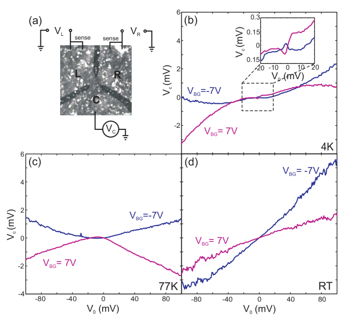
The measurement circuit used to investigate the voltage rectification properties of the three-terminal junction in the non-linear response regime is shown in Fig. 2(a). In order to avoid contact resistances and to ensure that the bias voltages are applied symmetrically to the device we have two Ohmic contacts at each branch of the junction and use the sense function of the DC voltage source to monitor the potential at one contact and apply the potential at the second contact. The voltages plotted in Figs. 2(b)-(d) are the measured voltages and not the applied voltages, which are larger since they partially drop across the contacts. With this setup we also eliminate possible non-linearities of the contacts themselves.
Figs. 2(b)-(d) shows the measurement of as a function of for backgate voltages +7 V (electrons) and -7 V (holes) at 4 K, 77 K and room temperature, respectively. As a general trend we see that as a function of always bends down for V and always bends up for V. At 4 K additional kinks can be seen in the curves for mV (see the inset in Fig. 2 (b)). This is due to universal conductance fluctuations (UCFs) and has been theoretically predicted csontos2003 . The linear part of as a function of is due the asymmetry of the device, which strongly depends on .
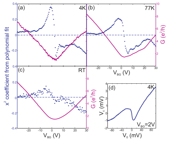
In the following we will have a closer look at the backgate dependence of the rectification signal. From the simple model shown in Fig. 1(c) it is expected that the vs curves always bend down for electrons and bend up for holes as confirmed in Figs. 2(b)-(d). However, it is also expected that the magnitude of curvature will decrease with increasing Fermi energy, meaning that the further the device is tuned away from the Dirac point the weaker the curvature is since the relative difference between the conductances left and right of the junction is small compared to the overall conductance. In Figs. 3(a)-(c) the magnitude of curvature (blue dots) and the conductance from the left lead to the right lead (pink curve) is plotted as a function of at 4 K, 77 K and room temperature, respectively. Here we have defined the magnitude of curvature as the second-order coefficient obtained from fitting the vs curve with a third order polynomial. It can be clearly seen that for holes the curvature is positive and for electrons it is negative, in agreement with the individual measurements shown in Figs. 2(b)-(d). Measuring the device in any of the two other possible measurement configurations gives qualitatively the same results. For holes it can be seen that the magnitude of curvature decreases while going to higher charge carrier densities as expected, however for electrons the curvature first decreases and then increases with increasing charge carrier density. We attribute this to inhomogenities in the sample leading to different charge neutrality points at different locations in the sample and therefore a mixture of electron and hole transport. This is supported by the kinks seen in the vs curves, for instance the kink at approximately +20 V backgate in Fig. 3(b). In addition it can be seen that as a general trend the magnitude of curvature decreases with increasing temperature, which is due to thermal smearing around the Fermi energy. Close to the Dirac point the vs curves cannot be fitted well presumably because of electron-hole puddles and strong disorder (see the example depicted in Fig. 3(d)) martin2008 .
For the measurements presented in this paper a voltage rectification of a few percent is obtained. According to our model the amount of rectification increases when the Fermi energy decreases and the difference in relative conductance between the left and the right constriction increases. To improve the rectification properties of the nanojunctions one possibility is therefore to make the devices smaller in order to open a transport gap and then tune the Fermi energy to a point close to the gap.
To conclude, we have observed voltage rectification up to room temperature in a diffusive graphene nanojunction when operated in the non-linear transport regime. Tuning the device from electron to hole transport the sign of rectification is switched.
We thank T. Ihn for helpful discussions and the Swiss National Science Foundation (SNF) for financial support.
References
- (1) A. K. Geim, Science 324, 1530 (2009)
- (2) H. Q. Xu, Appl. Phys. Lett. 78, 2064 (2001)
- (3) L. Worschech, H. Q. Xu, A. Forchel, and L. Samuelson, Appl. Phys. Lett. 79, 3287 (2001)
- (4) I. Shorubalko, H. Q. Xu, I. Maximov, P. Omling, L. Samuelson, and W. Seifert, Appl. Phys. Lett. 79, 1384 (2001)
- (5) Andrew N. Jordan and Markus B ttiker, Phys. Rev. B 77, 075334 (2008)
- (6) A. M. Song, A. Lorke, A. Kriele, J. P. Kotthaus, W. Wegscheider, M. Bichler, Phys. Rev. Lett. 80, 3831 (1998)
- (7) A. M. Song, P. Omling, L. Samuelson, W. Seifert, I. Shorubalko, and H. Zirath, Jap. J. of Appl. Phys. 40, L909, (2001)
- (8) A. M. Song, P. Omling, L. Samuelson, W. Seifert, I. Shorubalko, H. Zirath, Appl. Phys. Lett. 79, 1357 (2001)
- (9) I. Shorubalko, H. Q. Xu, P. Omling, L. Samuelson, Appl. Phys. Lett. 83, 2369 (2003)
- (10) D. B. Suyatin, J. Sun, A. Fuhrer, D. Wallin, L. E. Fr berg, L. S. Karlsson, I. Maximov, L. R. Wallenberg, L. Samuelson, and H. Q. Xu, Nano Lett. 8, 1100 (2008)
- (11) C. Papadopoulos, A. Rakitin, J. Li, A. S. Vedeneev, J. M. Xu, Phys. Rev. Lett. 85, 3476 (2000)
- (12) I. Shorubalko, H. Q. Xu, I. Maximov, D. Nilsson, P. Omling, L. Samuelson, W. Seifert, IEEE Electron Device Lett. 23, 377 (2002)
- (13) H. Q. Xu, I. Shorubalko, D. Wallin, I. Maximov, P. Omling, L. Samuelson, W. Seifert, IEEE Electron Device Lett. 25, 164 (2004)
- (14) C. R. Muller, L. Worschech, P. Hopfner, S. Hofling, A. Forchel, IEEE Electron Device Lett. 28, 859 (2007)
- (15) H. Sun, D. Wallin, I. Maximov, H. Q. Xu, IEEE Electron Device Lett. 29, 540 (2008)
- (16) S. Reitzenstein, L. Worschech, A. Forchel, IEEE Electron Device Lett. 25, 462 (2004)
- (17) B. Lau, D. Hartmann, L. Worschech, A. Forchel, IEEE Trans. on Electron Devices 53, 1107 (2006)
- (18) J. Mateos, B. G. Vasallo, D. Pardo, T. Gonzalez, J. S. Galloo, Y. Roelens, S. Bollaert, A. Cappy, Nanotechnology 14, 117 (2003)
- (19) K. I. Bolotin, K. J. Sikes, J. Hone, H. L. Stormer, and P. Kim, Phys. Rev. Lett. 101, 096802 (2008)
- (20) F. Schedin, A. K. Geim, S. V. Morozov, E. W. Hill, P. Blake, M. I. Katsnelson, and K. S. Novoselov, Nat. Mat. 6, 652 (2007)
- (21) W. J. Yu, U. J. Kim, B. R. Kang, I. H. Lee, E. H. Lee, and Y. H. Lee, Nano Lett. 9, 1401 (2009)
- (22) D. A. Areshkin and C. T. White, Nano Lett. 7, 3253 (2007)
- (23) K. S. Novoselov, A. K. Geim, S. V. Morozov, D. Jiang, Y. Zhang, S. V. Dubonos, I. V. Grigorieva, and A. A. Firsov, Science 306, 666 (2004)
- (24) A. C. Ferrari, J. C. Meyer, V. Scardaci, C. Casiraghi, M. Lazzeri, F. Mauri, S. Piscanec, D. Jiang, K. S. Novoselov, S. Roth, and A. K. Geim, Phys. Rev. Lett. 97, 187401 (2006)
- (25) D. Graf, F. Molitor, K. Ensslin, C. Stampfer, A. Jungen, C. Hierold, and L. Wirtz, Nano Lett. 7, 238 (2007)
- (26) D.Csontos and H. Q. Xu, Phys. Rev. B 67, 235322 (2003)
- (27) J. Martin, N. Akerman, G. Ulbricht, T. Lohmann, J. H. Smet, K. von Klitzing and A. Yacoby, Nat. Phys. 4, 144 (2008)