Resonant tunneling through superconducting double barrier structures in graphene
Abstract
We study resonant tunneling through a superconducting double barrier structure in graphene as a function of the system parameters. At each barrier, due to the proximity effect, an incident electron can either reflect as an electron or a hole (specular as well as retro Andreev reflection in graphene). Similarly, transport across the barriers can occur via electrons as well as via the crossed (specular and/or retro) Andreev channel, where a hole is transmitted nonlocally to the other lead. In this geometry, in the subgap regime, we find resonant suppression of Andreev reflection at certain energies, due to the formation of Andreev bound levels between the two superconducting barriers, where the transmission probability for electrons incident on the double barrier structure becomes unity. The evolution of the transport through the superconducting double barrier geometry as a function of the incident energy for various angles of incidence shows the damping of the resonance as normal reflection between the barriers increases.
pacs:
73.23.-b,72.80.Vp,74.45.+cI Introduction
The discovery of graphene, a two dimensional single layer of graphite, by K. S. Novoselov et al. novoselovetal1 a few years ago, has led to an upsurge in the study of its transport properties, both theoretically and experimentally geimreview ; castronetoreview ; sdsharmareview . In graphene, there are six discrete points at the edges of the hexagonal Brillouin zone where the energy bands touch the Fermi energy, out of which, only two are inequivalent and are commonly known as the and valleys. The low energy quasiparticle excitations about the and valleys behave like massless relativistic Dirac fermions. The presence of such quasiparticles in graphene provide us with an experimental test bed for observing many well-known phenomena in relativistic quantum mechanics, such as the Klein paradox katsnelson at low energies.
The existence of Dirac-like quasiparticles in graphene has also motivated a lot of research work in exploring the effects due to the proximity of a superconductor. Graphene is not a natural superconductor by itself. However superconductivity in a graphene layer can be induced in the presence of a superconducting electrode near it via the proximity effect hubert . A direct manifestation of proximity effect is the phenomenon of Andreev reflection (AR) andreev in which an electron like quasi-particle incident on a normal metalsuperconductor (NS) interface is reflected back as a hole along with the transfer of two electrons into the superconductor as a Cooper pair. Recently it has been predicted that a graphene NS junction, due to the presence of the Dirac-like energy spectrum of its quasiparticles, can exhibit specular Andreev reflection (SAR) beenakker1 ; beenakkerreview , in addition to the usual retroreflection observed in conventional NS junctions blonder . The presence of the SAR process in graphene leads to qualitatively different behaviour in the tunneling conductance subhro ; moitri1 ; linder1 ; linder2 , the Josephson current beenakker2 ; moitri2 and the spin current greenbaum as compared to those in conventional superconducting hybrid junctions.
An even more intriguing example where the proximity effect manifests itself is the phenomenon of crossed Andreev reflection (CAR) which can only take place in a normal metalsuperconductornormal metal (NSN) junction, provided the distance between the two normal metals is less than or equal to the phase coherence length of the superconductor. This is a nonlocal process where an incident electron from one of the normal leads pairs up with an electron from the other lead to form a Cooper pair and jumps into the superconductor. Due to the presence of the Dirac-like energy spectrum, like SAR , graphene can also exhibit specular crossed Andreev reflection (SCAR) in a proximity induced graphene NSN junction. The effect of CAR in graphene has been studied earlier in Refs. cayssol, ; cbenjamin, in the context of detecting entangled states in graphene. However, transport properties of a superconducting double barrier (SDB) geometry in graphene, i.e. graphene NSNSN junctions, have not been studied so far, where resonance effects can be more important.
In general, electronic confinement in graphene is experimentally challenging due to the effect of Klein tunneling. In the recent past, resonant tunneling has been considered in doped graphene (single barrier) -- junctions vfalko1 and in normal double barrier structures peeters ; baizhang where resonance effects on the transmission have been investigated. But here again, the problem of resonant transmission through doped double barriers in graphene has not been investigated. Motivated by this, in this article, we study resonant tunneling through a SDB structure in graphene, which, because of the correspondence between AR and Klein tunneling beenakker3 would also be valid for a doped graphene ---- junction.
The paper is organized as follows. In Sec. II, we describe the set-up for our system, where two superconducting patches have been deposited on top of a clean graphene sheet to form the graphene SDB structure and discuss its theoretical modeling. In Sec. III, we obtain the resonance condition analytically (the Andreev bound state condition) by considering multiple (retro) Andreev reflections between the barriers. Then in Sec. IV, we discuss the effect of normal reflection and SAR between the barriers on the resonances for angles of incidence other than normal incidence. In Sec. V, we discuss the numerical results of our study and show how the resonances behave as a function of the various parameters in the theory and also how the resonances evolve as a function of the energy for various values of the incident angle. Finally in Sec. VI, we present our summary and conclusions.
II Graphene SDB structure
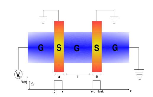
In our analysis, we consider a clean graphene sheet occupying the - plane. The SDB structure is formed by depositing thin strips of superconducting material on top of the graphene sheet at two places. This induces a finite superconducting gap () in the barrier regions as a result of the proximity effect of the superconducting patches. Here and are the pair potentials and order parameter phases on the two patches respectively ( refers to the index of the strips). The geometry is shown in Fig. 1. The space dependence of the order parameter (which also acts as a scattering potential for the incident electron) can be expressed as
| (1) | |||||
where is the width of the superconducting barrier in graphene and is the distance between the two barriers. Here we assume that the spatial variation of potential steps is slow on the scale of the lattice spacing so that inter-valley scattering is suppressed. Also here is the Heaviside -function, and we have taken , since we will not be looking at supercurrents (Josephson effect) in this work.
If the width of the superconducting strips is of the order of the phase coherence length of the superconductors, the normally incident electron can be transmitted across the barriers both as an electron (electron cotunneling (CT)) and as a hole, via the retro crossed Andreev reflection (CAR) process which is nonlocal and occurs between the same bands. Importantly, besides local retro AR and nonlocal retro CAR, graphene can also exhibit local specular Andreev reflection (SAR) and nonlocal specular crossed Andreev reflection (SCAR) cbenjamin which can switch the valley bands. In the process of retro CAR, an electron incident on the barriers is transmitted as a hole which retraces the trajectory of the incident electron. On the other hand, in SCAR, a hole is transmitted nonlocally but in a specular fashion. Here, we restrict ourselves to spin singlet (-wave) superconductors so that the electron and the hole are taken from opposite spin bands in order to allow the Cooper pair to jump into the superconductor with net spin zero.
Because of the pseudo spin and valley degeneracies present in graphene, it suffices to use a four dimensional version of the Dirac-Boguliobov-de Gennes equation (DBDG) beenakker1 for electrons and holes which is given by
| (8) |
where, , and the energy is measured from the Fermi level of the superconductor. We assume that in the normal graphene region and , a constant, independent of in the proximity induced superconducting region. Note that we have defined dimensionless variables
| (9) |
to replace the original ones.
The solution of the DBDG equations beenakker1 , describing electrons and holes with incident energy inside the normal graphene regions (), can be written as
| (14) |
| (19) |
where , and . is the angle of incidence of the incoming electron (with wave-vector ) and is the angle of reflection of the Andreev reflected hole (with wave-vector ). For retro AR, have opposite signs from whereas for SAR, they have the same signs. The change from retro () to SAR () occurs at (in our dimensionless units).
Similarly for the superconducting barrier regions, the four component spinor solutions contain electron wave-functions of one valley and hole wave-functions of the other valley. The DBDG equation can now be solved for any arbitrary energy and the four solutions inside the superconducting barriers are given in the preprint version of Ref. beenakker1,
| (24) |
| (29) |
where the subscripts refers to the upper and lower signs on the RHS respectively, and similarly for and
| (30) |
and
| (31) | |||||
Here, we have not taken the limit . We have also obtained the solution for both right-moving and left-moving electrons and holes.
Our aim now is to obtain the net quantum mechanical amplitudes for reflection, transmission, AR (and SAR) and CAR (and SCAR) of an electron incident on the SDB structure, after it has traversed both the barriers. A double barrier structure can always lead to resonances and this can affect the transmissions and the reflections through the system. For non-relativistic electrons, this scenario has been studied before morpurgo ; arijitkundu . For relativistic electrons, the standard paradigm is that one cannot obtain confined carrier states for normal incidence katsnelson ; beenakker1 due to Klein tunneling. However, discrete energy levels can be found for carriers in graphene based quantum wires, as long as they have a non-zero component parallel to the barrier peeters . Moreover, for normal incidence, discrete Andreev bound levels are also found between two superconductors in graphene beenakker2 ; moitri2 . These levels can clearly lead to resonant transmissions in a SDB structure in graphene.
We now follow the procedure set up in Ref. arijitkundu, and write a -matrix whose elements denote the various net reflection and transmission amplitudes, except that now the electron and hole wave-functions, and consequently, the transmission and reflection matrices are each of them also 4-component. Hence, the -matrix for the SDB structure in graphene for an incident electron with energy can be written as
| (32) |
where stands for normal reflection of electrons or holes and represents AR (and SAR), which is the reflection of an electron as a hole or vice-versa, from both the barriers combined. Similarly, represents CT or normal transmission amplitude of electrons or holes while corresponds to the non local CAR (and SCAR) amplitude for electron to hole conversion across the SDB structure. As mentioned earlier, each of these amplitudes are themselves matrices. The numerical results for these amplitudes can be obtained by matching the electron and hole wave-functions between the normal and proximity induced superconducting graphene at each of the four interfaces and the numerical results for the resonances are discussed in Sec. V.
III Andreev bound levels
Andreev bound states are formed due to multiple Andreev reflections (for non zero incidence angle, by multiple retro andreev reflections only). Let us first consider the AR matrices which converts electrons to holes at each interface. The elements of the AR matrix can be derived using
| (33) |
Each of this conditions gives two equations, and we have only 8 non zero elements in the matrix if there is no reflection. More explicitly, the matrix elements are:
| (34) |
The other elements of the matrix are found by interchanging , and also changing their positions to the other off-diagonal block. In particular, for , the matrix is much more simple and can be written as:
| (39) |
Note that needs to be small in order to ensure that the reflection is mainly retro-reflection. We will consider the effect of specular reflection (along with SAR) in the next section. In our analysis we have used left-right symmetry, but we have been careful to maintain the distinction between electron and hole parameters, since exact electron-hole symmetry only exists at . At any finite energy, the symmetry is broken.
We can also write down the transmission matrix which allows for both normal transmission and CAR through a single barrier. This matrix is defined by
| (40) |
and we find that the matrix elements are given by
| (41) |
Clearly includes both normal transmission and CAR. It is also clear that can be written as where is a matrix with two non-zero diagonal blocks and is a matrix with two non-zero non-diagonal blocks.
The phase matrix relating the electron and hole wave-function when it traverses the normal graphene region through a distance (the distance between the two superconductors) is given by
| (42) |
where
| (43) |
and is a diagonal matrix with the entries () denoting the phases picked up by the left and right moving electrons and holes respectively. The and matrices which rotate the momentum operator to an arbitrary basis are given by
| (44) |
with
| (45) |
The condition for resonance or for a bound state in the normal graphene region between the two superconductors is now just the condition that the total transmission computed as
| (46) | |||||
has a vanishing denominator. This is precisely the condition for the Andreev bound states formed by retro ARs without the presence of reflection. From this condition, one can find the corresponding Andreev bound state energy levels. Note that if we want the total transmission of electrons, we just need to replace by and if we want the total CAR of holes, we need to replace by . Both of them show the effect of the resonances.
IV Effect of reflection and SAR
For normal incidence in graphene, due to pseudo-spin symmetry, normal reflection is prohibited and we have pure Andreev bound states between the two superconductors. Normal bound states (formed by multiple ordinary reflections) are, in any case, not possible in graphene even at any other incident angle, when ordinary reflection is allowed. This is because multiple ordinary reflections are specular in nature and lead to a mode running along the -axis, rather than a bound state. This is also true even if we have SAR, which leads to a specular Andreev mode running along the -axis beenakkerreview .
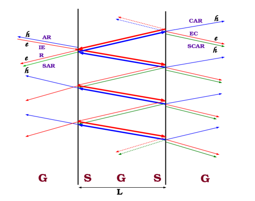
However, at a non-zero angle of incidence, if we have specular reflection present (Andreev as well as normal) at each graphene NS interface, we can still have Andreev bound states formed by multiple retro AR in between the two superconducting barriers. However, due to the specular nature of the reflection and the SAR, they are no longer localised. This is shown in Fig. 2. The incident electron can transmit through the first superconducting barrier as an electron and then have multiple retro AR. It can also have either ordinary reflection or SAR from the interface. The transmitted electron once again (in fact, for several times, depending on the length of the graphene sheet in the -direction) can have multiple retro AR before it is finally transmitted (or reflected) as an electron or a hole through the graphene SDB structure. The electron can also cross the first superconductor as a hole by retro CAR and then have multiple retro-reflections from the two interfaces and then this process can continue as well. The number of reflections (or SAR ’s) that can occur in a given sample is controlled by the length of the graphene sheet in the -direction and the angle of incidence of the electron. Naively, the number should go as , where is the length of the sheet in the -direction and and have already been defined earlier. In Fig. 2, we have only shown some of the possible quantum mechanical paths to emphasize how the Andreev bound states can form between the two barriers. We have also shown only a single incident electron, but the incident electron can also be at any point along the -axis. Hence, if we measure the total output current collected throughout the -length of the graphene sample, we should to able to get the signature of the many Andreev bound states present between the two superconducting barriers. In fact, the signatures of the Andreev bound states should be present in all the four amplitudes , , and , where these four amplitudes denote the quantum mechanical amplitudes for reflection, AR (SAR), transmission and CAR (SCAR) across the SDB structure for an incident electron. They should show either a maximum or a minimum precisely at the Andreev levels obtained in Eq. 46. This is the main point that we wish to emphasize in this paper. The Andreev levels can be obtained by measuring the transmissions and reflections through a SDB system even for large enough ; it does not require an effective ‘one-dimensional’ system. Furthermore, the signature of the resonances occurs in all the four amplitudes.
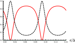
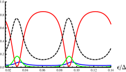
To illustrate the above argument, in Fig.3, we compare the positions of the resonances as a function of obtained by the vanishing of the denominator of Eq.46, the analytically obtained Andreev levels, (which do not include the effects of reflection) with the numerically obtained values of the conductance (by solving the scattering problem in the next section) for the same parameter values. Note that the numerical results do include reflection since we have chosen . Moreover, the numerical results include transmission throughout all points along the -axis (width of the graphene sheet). But as can be seen from the figure, the resonances still fall on top of each other. This clearly shows that the presence of specular reflection (and SAR) has no effect on the position of the resonances which simply occur due to the formation of the Andreev bound states discussed in the earlier section.
V Numerical results
In this section we describe the consequences of all the allowed quantum mechanical processes across the SDB geometry in graphene. To the left of the SDB structure, with an incident electron from the left, the wave-function can be written as
| (47) |
and to the right of the SDB structure, the wave-function can be written as
| (48) |
Here we use the standard wave-function matching technique to solve such scattering problems to obtain all the four quantum mechanical amplitudes. Hence matching the wavefunctions for the normal and proximity induced superconducting regions (Eq.(14-29)) at the four NS interfaces in graphene () forming the SDB structure, we obtain sixteen linear equations. Numerically solving these sixteen equations, we obtain the four amplitudes , , and , for the SDB structure, for an incident electron with energy below the gap . Note that we distinguish between electron and hole parameters, and hence the four amplitudes will be different for incident electrons and holes.
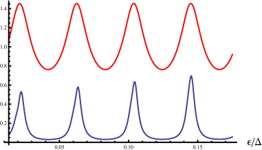
In our numerical analysis we do not distinguish between the specular and retro Andreev reflections and we also allow for normal reflection at each NS interface in graphene, besides normal transmission and CAR (specular and retro). The numerical results clearly show that for normal incidence of electron (), the net normal transmission (CT) and the net AR show resonant behaviour in the subgapped () regime. This is shown in the first panel in Fig. 4 and is precisely what one would expect, because for normal incidence due to the pseudo-spin symmetry, and this also leads to . For normally incident electrons, this kind of resonant behaviour is completely forbidden in a normal double barrier (DB) structure in graphene due to the phenomenon of Klein tunneling. This is the striking difference between a normal DB and a SDB in graphene.
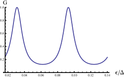
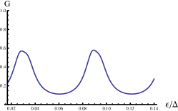
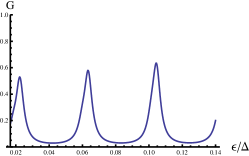
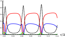
We also vary the momentum or equivalently the angle of incidence, and study the resonances in Fig. 3. As we have already mentioned, at or normal incidence, we have non-zero values only for and , and strong resonant behaviour for the transmission . As soon as the angle of incidence changes, we see the evolution of the and in the panels in Fig. 3. As we increase the angle of incidence, due to finite , normal reflection between the barriers increases, and due to the presence of both and between the barriers the amplitude of the transmission resonances decreases. However, at very large , the roles of reflection and Andreev reflection switch; this is true even for a single NS junction in graphene, since is proportional to and is proportional to beenakker1 . Hence, for large , we find large values of , but very small values of and once again, strong transmission resonances emerge.
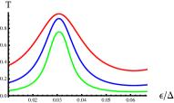
These resonances can also be tuned by varying parameters such as the ratio of the width of the superconductor to the length between the two superconducting barriers . As increases, we find that the resonances become sharper, and the distance between consecutive resonances increases. The behaviour of the resonances as a function of is shown in Figs 4(a) and 4(b).
The net angle-resolved differential conductance through the SDB system is now given by
| (49) |
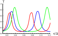
where is the number of input channels or transverse modes in a graphene sheet of width , is the unit of conductance and the factor of 4 comes from the pseudo-spin and valley degeneracies present in graphene. In our numerical analysis we have considered the temperature to be zero and also assumed linear bias. We again wish to emphasise the fact that since multiple Andreev reflections between the two superconducting barriers not only include both specular and retro AR, but also normal reflections, the exit point from the second superconductor can be anywhere along the width (-axis) of the graphene sheet. Therefore, both normal reflection as well as SAR can change the position of the transmitted beam along the -axis at each reflection. Hence, the total transmission here includes transmission at all points along . In other words, the output lead has also to be as wide as the graphene sheet. In Fig. 5, we show the net angle resolved Landauer-Buttiker conductance, given in Eq. 49, (for ) as a function of the energy of the incident electron , where again, the resonant behaviour can be seen for different values of or the incident angle. The behaviour of the conductance, also shows how the Andreev levels evolve as a function of the incident angle, showing that the height of the resonances is large when the multiple reflection between the barriers is either dominated by retro AR (small angles) or normal reflection (large angles).
VI Summary and Discussions
To summarize, in this paper, we have computed the transmission of an electron through a SDB structure in graphene and shown the resonant suppression of Andreev reflection at certain energies below the superconducting gap where normal transmission becomes unity. This resonant behaviour is absent in a normal double barrier in graphene due to Klein tunneling. We also show that the resonant suppression is due to the formation of Andreev bound states between the two superconducting barriers. Even at finite incident angles, the position of these Andreev bound levels remain unchanged in presence of reflection and SAR. Although, the transmission resonances get damped as the incident angle increases due to reflection and SAR. However, at large angles, the roles of AR and ordinary reflection get reversed, and once again, we see strong transmission resonances. The point that we wish to emphasize is that at any angle of incidence, all four transmission and reflection amplitudes, as well as the total conductance, shows strong signals of the Andreev bound states. We have also studied the resonances as a function of the ratios of the width of the superconducting barriers and the length of the normal graphene region between the two superconducting barriers. The most interesting study is the evolution of the resonances as a function of , the momentum in the -direction or equivalently the angle of incidence of the incoming electron.
As far as the practical realization of such a SDB structure in graphene is concerned, it should be possible to fabricate such a geometry by depositing thin strips of a spin singlet superconductor (like or ) on top of a graphene sheet hubert at two places. The width of the strips should be of the order of the superconducting phase coherence length ( in case of ) for CT and CAR (and SCAR) to take place. For a given ratio, the resonance in this SDB geometry can be tuned by varying the energy of the incident electron (which can be done by applying a small bias voltage between the two reservoirs keeping within linear response, so that our calculations are valid). In Fig. 4(a) and 6(a), the equivalent temperature at which the first resonance occurs is approximately (critical temperature in case of ) for and .
Note also that, experimentally, it is not easy to control the angle of incidence of the electrons that impinge on the SDB structure. In fact, for a given sample what can possibly be done is to grow the barriers at different tilted positions by lithographic techniques which allows the electrons to be incident on the barriers at different angles. However, in a given experiment, the angle of the incident electron is fixed, since the incident electrons are collimated. Therefore different experiments need to be performed with ballistic graphene samples to obtain results at different angles of incidence. In a given experiment, the angular spread of the incident electrons which would exist due to lack of perfect collimation is actually quite small, hence even after angular averaging our results at a given angle should qualitatively remain the same.
We also expect the features of the resonances to be qualititavely unaffected by long-ranged impurities (slow on the scale of the lattice spacing i.e. where , is the lattice spacing and is the mean-free path of electron in graphene), because such impurities in graphene can only cause intra-valley scattering. On the other hand, short range impurities () can cause intervalley scattering which can destroy the resonance. Also, strong disorder can localize electron/hole states between the two barriers which always can destroy the resonance. Another experimental variable which is expected to destroy the resonance is the presence of a magnetic field which bends the electron paths between the two barriers. Hence, it prevents the multiple retracing of the path, which is needed for resonance. Therefore, we do not expect resonances in the presence of strong disorder or even weak magnetic fields.
In this work, we have restricted ourselves to rectangular barriers, whereas experimentally, the barriers are expected to be smoother phillipkim . As shown in the references by Cayssol et al. cayssol1 and Sonin sonin , the transmissions are affected by the shape of the potential, and it is shown that the resonances for normal double barriers in graphene are sharpened by smoother barriers. By analogy, we expect our resonances to be sharpened if we make the barriers smooth instead of using rectangular barriers. Nevertheless, to check it explicitly, we need to repeat the calculations for other shapes of barriers which is beyond the scope of this paper.
From the application point of view, this SDB geometry also can be used to confine electrons in graphene which is experimentally very challenging due to Klein tunneling. The resonant structure of as a function of is analogous to the Coulomb blockade peaks of a quantum dot. Hence, this kind of SDB geometry can be used to form quantum dots in graphene. Another interesting point which can be mentioned is that this kind of proximity induced SDB geometry can also be obtained by replacing the graphene sheet by a 2D Quantum Spin Hall topological insulator. The only difference will be the replacement of the factor of in the Landauer-Buttiker conductance formula by unity, since there are no pseudo-spin or valley degeneracies present in such quantum spin Hall insulator.
Acknowledgements.
The work of A.S. was supported by the Feinberg fellowship programme at WIS, Israel. One of us (A.S.) acknowledge Anindya Das for useful discussions and comments. One of us (S.R.) would also like to acknowledge hospitality at the Perimeter Institute for Theoretical physics, Canada, where this work was completed.References
- (1) K. S. Novoselov, A. K. Geim, S. V. Morozov, D. Jiang, Y. Zhang, S. V. Dubonos, I. V. Grigorieva, and A. A. Firsov, Science 306, 666 (2004).
- (2) A. K. Geim and K. S. Novoselov, Nat. Materials 6, 183 (2007).
- (3) A. H. Castro Neto, F. Guinea, N. M. R. Peres, K. S. Novoselov, and A. K. Geim, Rev. Mod. Phys. 81, 109 (2009).
- (4) S. D. Sarma, S. Adam, E. H. Hwang, and E. Rossi, Electronic transport in two dimensional graphene (2010), arXiv:1003.4731 [cond-mat.mes-hall].
- (5) M. I. Katsnelson, K. S. Novoselov, and A. K. Geim, Nat. Phys. 2, 620 (2006).
- (6) H. B. Heersche, P. J. Herrero, J. B. Oostinga, L. M. K. Vandersypen, and A. F. Morpurgo, Nature 446, 56 (2007).
- (7) A. F. Andreev, Sov. Phys. JETP 19, 1228 (1964).
- (8) C. W. J. Beenakker, Phys. Rev. Lett. 97, 067007 (2006).
- (9) C. W. J. Beenakker, Rev. Mod. Phys. 80, 1337 (2008).
- (10) G. E. Blonder, M. Tinkham, and T. M. Klapwijk, Phys. Rev. B 25, 4515 (1982).
- (11) S. Bhattacharjee and K. Sengupta, Phys. Rev. Lett. 97, 217001 (2006).
- (12) S. Bhattacharjee, M. Maiti, and K. Sengupta, Phys. Rev. B 76, 184514 (2007).
- (13) J. Linder and A. Sudbø, Phys. Rev. Lett. 99, 147001 (2007).
- (14) J. Linder and A. Sudbø, Phys. Rev. B 77, 064507 (2008).
- (15) M. Titov and C. W. J. Beenakker, Phys. Rev. B 74, 041401(R) (2006).
- (16) M. Maiti and K. Sengupta, Phys. Rev. B 76, 054513 (2007).
- (17) D. Greenbaum, S. Das, G. Schwiete, and P. Silvestrov, Phys. Rev. B 75, 195437 (2007).
- (18) J. Cayssol, Phys. Rev. Lett. 100, 147001 (2008).
- (19) C. Benjamin and J. K. Pachos, Phys. Rev. B 78, 235403 (2008).
- (20) V. V. Cheianov and V. I. Falko, Phys. Rev. B 74, 041403(R) (2006).
- (21) J. M. Pereira, P. Vasilopoulos, and F. M. Peeters, Appl. Phys. Lett. 90, 132122 (2007).
- (22) C. Bai, Y. Yang, and X. Zhang, Physica E 42, 1431 (2009).
- (23) C. W. J. Beenakker, A. R. Akhmerov, P. Recher, and J. Tworzydlo, Phys. Rev. B 77, 075409 (2008).
- (24) A. F. Morpurgo and F. Beltram, Phys. Rev. B 50, 1325 (1994).
- (25) A. Kundu, S. Rao, and A. Saha, Euro. Phys. Lett. 88, 57003 (2009).
- (26) A. F. Young and P. Kim, Nat. Phys. 5, 222 (2009).
- (27) J. Cayssol, B. Huard, and D. Goldhaber-Gordon, Phys. Rev. B 79, 075428 (2009).
- (28) E. B. Sonin, Phys. Rev. B 79, 195438 (2009).