Photonic circuits for generating modal, spectral, and polarization entanglement
Abstract
We consider the design of photonic circuits that make use of Ti:LiNbO3 diffused channel waveguides for generating photons with various combinations of modal, spectral, and polarization entanglement. Down-converted photon pairs are generated via spontaneous optical parametric down-conversion (SPDC) in a two-mode waveguide. We study a class of photonic circuits comprising: 1) a nonlinear periodically poled two-mode waveguide structure, 2) a set of single-mode and two-mode waveguide-based couplers arranged in such a way that they suitably separate the three photons comprising the SPDC process, and, for some applications, 3) a holographic Bragg grating that acts as a dichroic reflector. The first circuit produces two frequency-degenerate down-converted photons, each with even spatial parity, in two separate single-mode waveguides. Changing the parameters of the elements allows this same circuit to produce two nondegenerate down-converted photons that are entangled in frequency or simultaneously entangled in frequency and polarization. The second photonic circuit is designed to produce modal entanglement by distinguishing the photons on the basis of their frequencies. A modified version of this circuit can be used to generate photons that are doubly entangled in mode number and polarization. The third photonic circuit is designed to manage dispersion by converting modal, spectral, and polarization entanglement into path entanglement.
Mohammed F. Saleh,1 Giovanni Di Giuseppe,2,3 Bahaa E. A. Saleh,1,2
and Malvin Carl Teich,1,4,5
1Quantum Photonics Laboratory, Department of Electrical & Computer Engineering, Boston University, Boston, MA 02215 USA
2Quantum Photonics Laboratory, College of Optics and Photonics (CREOL), University of Central Florida, Orlando, FL 32816 USA
3School of Science and Technology, Physics Division, University of Camerino, 62032 Camerino (MC), Italy
4Department of Physics, Boston University, Boston, MA 02215 USA
5Department of Electrical Engineering, Columbia University, New
York, NY 10027 USA
1 Introduction
Entanglement in a pair of photons can be manifested in degrees of freedom that are discrete, such as polarization [1], or in degrees of freedom that are continuous, such as spectral or spatial [2, 3, 4, 5]. However, a continuous degree of freedom may be binarized by selection of a pair of values, as in path entanglement [6, 7], or, as in orbital-angular-momentum entanglement [8], by expansion in some basis while retaining only two basis functions [9]. Alternatively, in place of truncation, the space of continuous functions of position may be mapped onto a binary set of even and odd functions, as in spatial-parity entanglement [10, 11, 12]. We recently investigated the possibility of using spontaneous parametric down-conversion (SPDC) in two-mode planar and circular waveguides to generate guided-wave photon pairs entangled in mode number [13]. If the photons are confined in this manner, the spatial variables are naturally binarized and can be used to represent a modal qubit [14].
In this paper, we consider the design of photonic circuits, based on Ti:LiNbO3 diffused channel waveguides, that generate photon pairs endowed with various combinations of modal, spectral, and polarization entanglement. The on-chip generation of such photon pairs can serve as a basic resource for one-way quantum computation [15], as well for linear optical quantum computing [16]. Down-converted photon pairs are generated via spontaneous parametric down-conversion (SPDC) in a two-mode waveguide using a CW pump source. The waveguide configuration confines the photons to a single direction of propagation. Any of the available degrees of freedom — mode number, frequency, or polarization — can be used to distinguish the down-converted photons while the others can serve as carriers of entanglement. We study a class of photonic circuits that comprises: 1) a nonlinear periodically poled two-mode waveguide structure; 2) a set of single- and two-mode waveguide-based couplers arranged in such a way that they suitably separate the three photons comprising the SPDC process; and, for certain applications, 3) a holographic Bragg grating.
A good deal of effort has been devoted to examining the properties of single-mode silica-on-silicon waveguide quantum circuits [17, 18], with an eye toward applications in quantum-information processing [19, 20, 21, 22, 23, 24]. For these materials, the photon-generation process necessarily lies off-chip, however. Single- and multi-mode potassium titanyl phosphate (KTiOPO4, KTP) waveguide structures have also been extensively studied for producing pulsed spontaneous parametric down-conversion [25, 26, 27, 28, 29], but it appears that only the generation process has been incorporated on-chip. Earlier, periodically poled lithium niobate (PPLN) waveguide structures were suggested for producing spontaneous parametric down-conversion [30] and the conditions required for generating counterpropagating entangled photons from an unguided pump field were established [31]. Furthermore, the generation of non-collinear and non-degenerate polarization-entangled photons via concurrent Type-I parametric down-conversion was demonstrated in a PPLN crystal [32].
The use of lithium niobate photonic circuits has a number of merits: 1) the properties of the material are well-understood since it has low loss and has long been the basis of integrated-optics technology [33], [34, Chap. 8]; 2) the material can easily be periodically poled [35, 36] for the purpose of phase matching parametric interactions. And, as we show in this paper: 3) circuit elements such as mode-separation components can readily be designed for two-mode waveguides; and 4) the generation, separation, and processing of entangled photons can all be accommodated on a single chip. Moreover, consistency between simulation and experimental measurement has been demonstrated in a whole host of configurations [37, 38, 39, 40, 41]. To enhance tolerance to fabrication errors, photonic circuits can be equipped with electro-optic adjustments. For example, an electro-optically switched coupler with stepped phase-mismatch reversal serves to maximize coupling between fabricated waveguides [42, 43].
The paper is organized as follows. In Sec. 2, the theory of modal entanglement in two-mode waveguides is reviewed. Section 3 is dedicated to examining the operation of a photonic circuit that produces a pair of frequency-degenerate photons at its output. As explained in Sec. 4, changing the parameters of the elements comprising the circuit considered in Sec. 3 allows it to produce nondegenerate down-converted photons that are entangled in frequency, or simultaneously entangled in frequency and polarization. The second photonic circuit, examined in Sec. 5, distinguishes the photons on the basis of their frequencies and provides means for generating modal entanglement and, with some modifications, modal and polarization double entanglement. The third photonic circuit, considered in Sec. 6, is designed to manage the deleterious effects of dispersion. The conclusion is provided in Sec. 7.
2 Generating modal entanglement in two-mode waveguides
The theory underpinning the generation of modal entanglement in waveguides has been recently described [13]. Entanglement arises from the multiple possibilities for satisfying energy and momentum conservation, as required by the parametric interaction process. In this section, we proceed to apply the theory provided in [13] to diffused channel Ti:LiNbO3 waveguides.
Consider a SPDC process in a periodically poled two-mode waveguide (TMW) structure, in which a cw pump wave propagating in the -direction is down-converted into a signal wave and an idler wave [34, Chap. 21]. The fundamental mode of this TMW () is even while the next-higher mode () is odd, where . We seek to generate an entangled state such that if the signal is in the even mode, then the idler must be in the odd mode, and vice versa.
The biphoton state is written as [13]
| (1) |
where the squared-magnitude of represents the SPDC spectrum associated with the component. The signal and idler mode numbers are and , their polarization indexes are and , and their angular frequencies are and , respectively, with . The angular frequency of the pump is denoted . For ease of display, the output spectra for the two possibilities represented by the quantities and are normalized to the maximum of their peak values. Moreover, these quantities are plotted only for signal frequencies above the degenerate frequency by virtue of the fact that .
This particular state requires that: 1) the pump mode be odd so that the spatial overlap integral does not vanish; and 2) the phase matching conditions of the two possibilities at the preselected frequencies and be satisfied, i.e.,
| (2) |
where ; ; is the propagation constant of wave ; and is the th-order uniform poling period. The efficiency of the interaction decreases by a factor for the th-order poling period with respect to the first-order one [44]. The choice of the TMW width determines the propagation constants of the interacting modes. The values of the waveguide width and poling period selected should ensure that these conditions are met or approximately met.
The indistinguishability between the down-converted photons is typically ascertained via a Hong–Ou–Mandel (HOM) interferometer [45, 46]. The rate of photon coincidences at a pair of detectors placed at the two output ports of the interferometer is given by [13]
| (3) |
where is the temporal delay between the down-converted photons and the asterisk denotes complex conjugation.
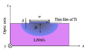
All of the simulations presented in this paper refer to structures that make use of Ti:LiNbO3 diffused channel waveguides, as illustrated in Fig. 1. These waveguides are fabricated by diffusing a thin film of titanium (Ti), with thickness nm and width , into a -cut, -propagating LiNbO3 crystal. The diffusion length is taken to be the same in the two transverse directions: m. The TE mode polarized in the -direction sees the ordinary refractive index , whereas the TM mode polarized in the -direction sees the extraordinary refractive index .
The ordinary and extraordinary refractive indexes may be calculated by making use of the Sellmeier equations [34, Chap. 5], [47, 48]. The refractive-index increase introduced by titanium indiffusion is characterized by , where and for and , respectively [49]. To accommodate wavelength dispersion, can be modified by incorporating the weak factor , where the wavelength is specified in m [50]. We calculate the effective refractive index of a confined mode in two ways: 1) by using the effective-index method described in [51]; and 2) by making use of the commercial photonic and network design software package RSoft. The propagation constant of a guided mode is related to via .
In the following sections, we consider several photonic circuits for the generation, separation, and control of down-converted photons. In Sec. 3, we consider a circuit that generates degenerate photons in separated single-mode waveguides. In this case, the two conditions specified in (2) collapse to a single condition since and . In Sec. 4, with a change of parameters, this same circuit is used to produce nondegenerate photons entangled in frequency or simultaneously entangled in frequency and polarization. Section 5 relates to photonic circuitry that produces nondegenerate photons distinguished by their frequencies, which leads to modal as well as modal and polarization double entanglement.
3 Photonic circuit for generating degenerate photons in different modes
This section is dedicated to examining the operation of a photonic circuit that produces a pair of down-converted photons, and then uses their differing spatial properties (mode numbers) to ultimately guide them into two separate, single-mode waveguides. The output provides a pair of degenerate photons that have even parity and can be fed into an HOM interferometer [45, 46] integrated on the same chip (see Sec. 6).
In particular, we consider the implementation of degenerate Type-0 SPDC in a TMW of width , wherein a pump photon with is split into a pair of down-converted photons with different spatial parities. The associated two-photon state is
| (4) |
where the two terms merge for the degenerate case, i.e., when . Figure 2(a) represents a photonic circuit that can be used to generate photon pairs of this type. The circuit comprises three sequential stages: a periodically poled region, an odd-mode coupler, and an even-mode coupler. We consider these three stages in turn.
The periodically poled stage shown in Fig. 2(b) is characterized by its width , length , and th-order poling period . For certain values of the width, there will always be a single value of the poling period that satisfies (2) so that there is flexibility in choosing the TMW width . Once the width is assigned, the poling period is determined via (2). There are no restrictions on the length of the nonlinear stage , save those associated with the process of fabrication. Increasing does, of course, increase the flux of photon pairs but we will see in the next Section that there is a limitation on how large can be made for generating entangled photons.
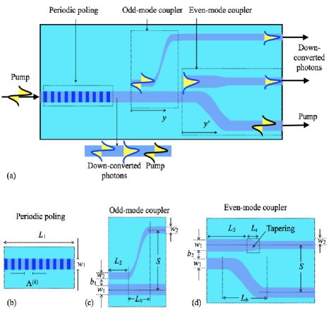
The odd-mode coupler is used to extract only the down-converted photon with an odd spatial distribution. Its principle of operation is based on selective coupling between adjacent waveguides of different widths. The even and odd modes of the TMW are characterized by different propagation constants. As depicted in Fig. 2(c), an auxiliary single-mode waveguide (SMW) with appropriate width , length , and separation distance from the TMW can be used to phase-match the odd-mode in the TMW to the even-mode in the SMW. Attached to the end of the SMW is an -bend waveguide in which the initial and final widths are both ; this obviates the possibility of further unwanted coupling to the TMW. In short, the odd-mode coupler distinguishes between the two down-converted photons based on their spatial profiles and delivers the initially odd-mode photon as an even-mode photon at its output.
The even-mode coupler is used to separate the down-converted photon with an even spatial profile from the pump wave. The principle of operation is based on the limited extent of the short-wavelength evanescent pump field, which precludes it from coupling to other waveguides of the same width located at typical distances. The result is that the even-mode down-converted photon alone is coupled into a second identical TMW, of length and separation distance from the original TMW, as shown in Fig. 2(d). The end of the second TMW is then coupled to a SMW of width via an adiabatically tapered waveguide region of length . The tapering offers two benefits: 1) the even mode of the TMW is transformed into an even mode that matches that of the partner photon at the output of the odd-mode coupler; and 2) unwanted odd modes inadvertently coupled in from external radiation are eliminated. The down-converted degenerate photons produced by this photonic circuit have the same mode number at the output, and can therefore interfere quantum mechanically [46]. It is worthy of mention that heralded single-photon pure states in well-defined spatiotemporal modes are required for many quantum information technology applications [14], such as quantum cryptography [52] and linear optical quantum computing [16].
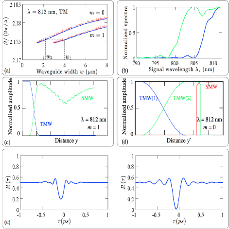
Figure 3 provides an example in which the performance of this photonic circuit is simulated. Figure 3(a) displays the dependencies of the fundamental and first-order mode propagation constants on the waveguide widths . These curves are used to select the widths of the TMW and SMW; the horizontal dotted line represents the loci of the phase-matching conditions between even and odd modes in waveguides of different widths. Figure 3(b) shows the normalized output spectra and as a function of the signal wavelength . As a consequence of the large phase mismatch between the interacting modes, the value for the first-order poling period turns out to be small, but values in this range have been realized using the method of surface poling in diffused channel waveguides [35]. Using a pump source of longer wavelength, such as 532 nm, would permit regular poling techniques to be used. A salutary feature is that the Type-0 interaction makes use of the strongest nonlinear component of the second-order tensor, , so that high efficiency is expected from this interaction [53]. Figures 3(c) and 3(d) display the evolution with distance of the normalized amplitudes of the interacting modes in the odd- and even-mode couplers, respectively. For the odd-mode coupler, the amplitude of the even excited mode in the SMW exhibits a dip that is associated with the tapered nature of the -bend. The values and 0 in Figs. 3(c) and 3(d), respectively, refer to the mode numbers at the point of generation. Figure 3(e) displays the dependencies of the normalized coincidence rate on the temporal delay , without insertion (left curve), and with insertion (right curve), of two narrowband filters at the degenerate frequency before the two output detectors. The reasons underlying the reduced visibility of the dip, and its displacement from , are considered in Sec. V of [13].
4 Photonic circuits for generating spectral and spectral / polarization entanglement
Changing the values of the parameters provided in Fig. 3 allows the circuit shown in Fig. 2 to produce two nondegenerate down-converted photons that are entangled in frequency, or simultaneously in frequency and polarization, via a Type-0 or Type-II interaction, respectively.
Using the mode numbers to distinguish the photons, (1) takes the form
| (5) |
However, some restrictions apply to the generation and separation portions of the circuit, as discussed in the following paragraphs.
With respect to the generation region, values of the waveguide width and poling period govern how the conditions in (2) are satisfied. Simulations show that: 1) for certain values of the waveguide width, slightly different poling periods are required to satisfy these conditions; and 2) the absolute difference between the quantities and , which appear in (2), is nearly independent of waveguide width. Consequently, the choice of can be left to other considerations, such as fabrication limitations and subsequent design requirements.
Our strategy is to satisfy the sum condition, rather than each condition individually, for a specified value of the waveguide width, so that
| (6) |
where . Substituting the value of the poling period obtained in both conditions of (2) leads to small errors in satisfying the phase-matching conditions for the two interactions. These errors can be used to determine the coherence lengths for the two interactions, which then provide upper bounds to the length of the periodically poled region . The choice of must also result in good spectral overlap between and around the preselected frequencies, since determines the widths of these functions. It turns out that this strategy leads to almost maximally entangled states at the preselected frequencies.
With respect to the coupling region, the design must optimize coupling at both preselected frequencies, and . The choice of and for the odd-mode coupler is based on satisfying the phase matching conditions between an odd mode in a TMW of width and an even mode in a SMW of width , for both and :
| (7) |
Since the down-conversion generation process depends only weakly on waveguide width, we select the TMW width in the generation region to be equal to ; this obviates the need to taper the waveguide from the periodically poled region to the odd-mode coupler. The coupling length is frequency and polarization dependent, however, so that the SMW length , in combination with the separation distance , must be carefully chosen to maximize the coupling for both and . The same considerations apply for the even-mode coupler, so that the second TMW length and separation distance are selected similarly.
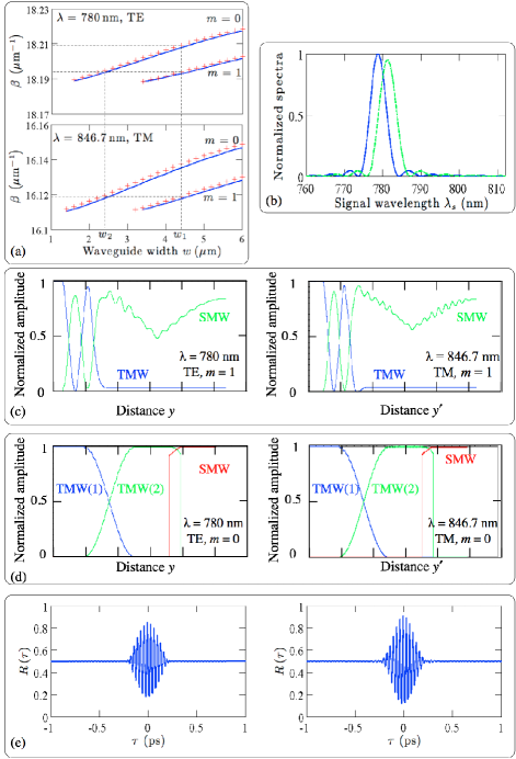
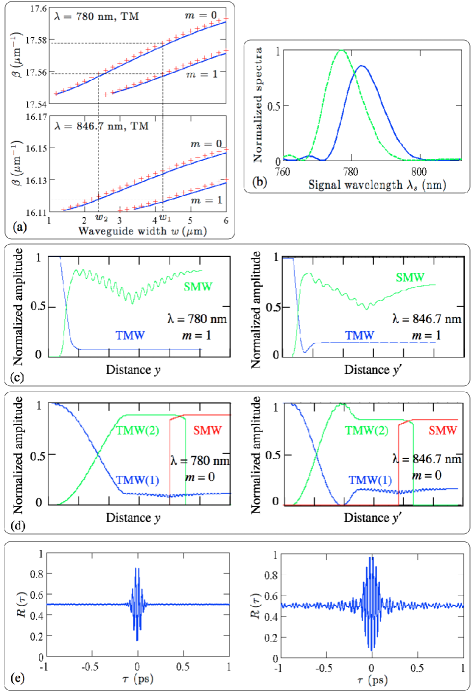
An example, provided in Fig. 4, illustrates the simulated performance of the photonic circuit shown in Fig. 2 for generating spectrally entangled photons. Consider nondegenerate Type-0 SPDC, in which a pump laser of wavelength 406 nm, in mode , generates two photons centered about the wavelengths 780 nm and 846.7 nm. The TMW width and the SMW width are determined via Fig. 4(a), which represents the dependencies of the propagation constants on waveguide width. The values and are chosen to satisfy (7) as closely as possible. Figure 4(b) displays the output normalized spectra, and , for an SPDC poling length that was selected to attain maximum entanglement and high efficiency. The performance of the odd- and even-mode couplers are displayed in Figs. 4(c) and 4(d), respectively; each panel contains plots for the two frequencies and . The values and 0 in Figs. 4(c) and 4(d), respectively, refer to the mode numbers at the point of generation, and the curves are color-coded in the same way as the corresponding curves in Fig. 3. The values of () and () are selected to optimize coupling of the odd (even) modes for both and . Figure 4(e) displays the behavior of the normalized coincidence rate function for the down-converted photons, without insertion (left curve), and with insertion (right curve), of two 10-nm narrowband filters, centered about 780 and 846.7 nm, before the two output detectors.
An example based on nondegenerate Type-II SPDC, illustrated in Fig. 5, suggests that simultaneous spectral and polarization entanglement can be obtained by again making use of the photonic circuit shown in Fig. 2. By convention, the notation indicates, in consecutive order, the polarization of the down-converted photon whose frequency lies above the degenerate frequency, the down-converted photon whose frequency lies below the degenerate frequency, and the pump photon. Type-II behavior is obtained by using a TE pump in place of the TM pump employed in Fig. 4, and by choosing the circuit-element parameters, including , appropriately. The panels displayed in Fig. 5 are similar to those shown in Fig. 4. Again, the values and 0 in Figs. 5(c) and 5(d), respectively, refer to the mode numbers at the point of generation, and the curves are color-coded in the same way as the corresponding curves in Figs. 3 and 4. In principle, spectral and polarization double entanglement [13] could also be attained with this arrangement, but the parameters that achieve it are not easily established.
5 Photonic circuits for generating modal and double modal / polarization entanglement
This section focuses on the operation of a photonic circuit that generates modal entanglement by distinguishing two nondegenerate photons on the basis of their frequencies, rather than their mode numbers. Modally entangled photons in a two-mode waveguide have the following property: a photon whose frequency lies above the degenerate frequency and appears in the fundamental (even) mode is always accompanied by another whose frequency lies below the degenerate frequency and appears in the first-order (odd) mode, and vice versa. Alternatively, the photons could be distinguished on the basis of their polarizations in the context of a Type-II configuration. When the photons are distinguished on the basis of their frequencies, the biphoton state (1) is written as
| (8) |
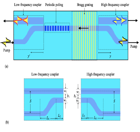
Modal entanglement is generated by the photonic circuit displayed in Fig. 6. It comprises three stages. The first periodically poled stage is a nonlinear region, as in Fig. 2(b), that produces a pair of nondegenerate down-converted photons via SPDC. As discussed in Sec. 3, this stage is characterized by its width , length , and th-order poling period . The choice of these parameters is governed by the same considerations as those attendant to the discussion in Sec. 4.
The second stage is a holographic Bragg grating that distinguishes the down-converted photons based on their frequency, such as by reflecting the low-frequency photon while transmitting the high-frequency photon so they travel in opposite directions. The third stage consists of two couplers that transfer the even and odd down-converted photons from the original waveguide in which they are generated to the output-port waveguides of the circuit, via a low-frequency coupler to the left and a high-frequency coupler to the right.
The holographic Bragg grating can be inscribed on the Ti:LiNbO3 waveguide by superposing two coherent plane waves and making use of proton exchange [54], or a dopant such as Cu together with thermal fixing [39]. The sinusoidal light-intensity pattern generated by the superposition of the plane waves [34, Chap. 2] is impressed on the waveguide as a sinusoidal modulation of the refractive index. The wavelength of light at which the reflected intensity is maximum (for normal incidence) is , where is the grating period and is the effective refractive index of the guided mode. The bandwidth of the reflected light decreases with increasing grating length. The fundamental and first-order modes can be reflected at a given wavelength by making use of either a single hologram of short length or two mutliplexed holograms of longer length. Multiplexing is most effectively achieved by recording the holograms sequentially [39].
The low- and high-frequency couplers are designed to couple the idler-frequency () and signal-frequency () photons, respectively, into separate output TMWs that exclude the pump, as shown in Fig. 6. This is achieved by bringing two auxiliary TMWs into proximity with the principal TMW; all are of the same width so the spatial profiles of both the even and odd modes can be maintained in the course of coupling. The pump fails to couple to these auxiliary TMWs because it has a short-range evanescent field by virtue of its high frequency. The lengths of the auxiliary TMWs, and their separation distances, are designed to optimize coupling of both the even and the odd modes. For the low-frequency (high-frequency) coupler, the auxiliary TMW is of length () and the separation distance is () from the principal waveguide, as illustrated in Fig. 6(b).
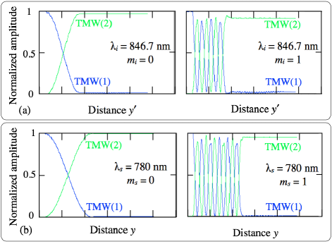
A simulation in which the photonic circuit in Fig. 6 is used to generate a pair of photons entangled in mode number is presented in Fig. 7. The nonlinear SPDC source is identical to that displayed in Fig. 4. The Bragg grating consists of two multiplexed holograms, with periods of 83.8 and 83.7 nm, to reflect the fundamental and first-order modes of the low-frequency down-converted photon, respectively. Figures 7(a) and 7(b) display the performance of the low- and high-frequency couplers, respectively. Each panel has two subplots, for the even () and odd modes (). For both frequencies, the coupling length of the first-order mode is substantially shorter than that of the fundamental mode since the peaks of the field for the former lie closer to the transverse edges of the waveguide. Since the coupling length is fixed, multiple cycles of energy transfer of the odd modes (right panels) are required to assure full coupling of the even modes (left panels).
A modified version of the photonic circuit displayed in Fig. 6 can also be used to generate photons, via a Type-II interaction, that are doubly entangled in mode number and polarization. The biphoton state in that case is
| (9) |
This interaction can be viewed as a superposition of Type-II and Type-II . To generate such doubly entangled photons, the periodically poled nonlinear region portrayed in Fig. 6 would have to be replaced by nonuniform (e.g., linearly chirped) poling, or aperiodic poling [55], to satisfy the phase matching conditions for the four possibilities. Also, the holographic Bragg grating would then have to consist of four multiplexed holograms of long length, or two multiplexed holograms of short length. Since the Bragg-grating outputs in both directions could be a photon in the fundamental- or first-order mode, with TE- or TM-polarization, the low- and high-frequency couplers would both have to be designed to optimize coupling for all of the possibilities. It is worthy of mention that states entangled in more than one degree of freedom are the primary resource for one-way computation [15].
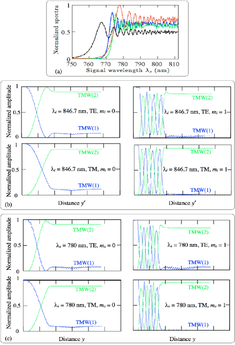
An example to illustrate the simulated performance of such a photonic circuit for generating photons that are doubly entangled in mode number and polarization is displayed in Fig. 8. As shown in Fig. 8(a), the use of linearly chirped poling leads to broadband spectra. The low-frequency photon would be filtered using the Bragg grating, while the high-frequency photon could be filtered by placing a narrowband filter at the output detector. The generation of narrowband spectra could, in principle, be achieved by making use of aperiodic poling; however, this would require poling periods so small that they might be beyond the capabilities of current fabrication techniques.
6 Photonic circuits for dispersion management
The presence of dispersion is deleterious to the operation of photonic circuits used for many quantum-information applications. Dispersion results from the dependence of the propagation constant on frequency, mode number, and polarization. Polarization-mode dispersion generally provides the strongest contribution, especially in a birefringent material such as LiNbO3. However, the Type-0 interaction, by virtue of its three parallel electric field vectors, suffers only from frequency and modal dispersion, and these are often sufficiently weak that they can be neglected for short devices. This is not the case for Type-II circuits, however, where polarization-mode dispersion is indeed dominant.
In this section, we address the management of dispersion and consider possible ways of mitigating it in photonic circuits, whatever the type of interaction. The optimal approach for circumventing dispersion depends on the particular application.
An example that proves instructive is the photonic-circuit HOM interferometer, in which a simple adjustment of the path length can be effective. The photonic circuit shown in Fig. 2 provides for the generation, separation, and guiding of two SPDC photons into two distinct SMW output ports. An HOM interferometer can be fabricated on the same chip by feeding these outputs into a 3-dB coupler endowed with an electro-optic phase modulator in one of its input arms. This allows a variable phase delay to be introduced between the photons, thereby enabling an interferogram to be generated.
The presence of dispersion alters the coincidence rate associated with the HOM interferometer. The origin of this effect can be understood by casting the interferometer as a four-port system with each arm behaving as an ideal phase filter. Referring to Fig. 2, the matrix that relates the output and input of the system then takes the form
| (10) |
with
| (11) |
where is the length of an arm of the 3-dB coupler; and are the distances traveled by the even and odd modes from the generation region to the 3-dB coupler, respectively; is the length of the tapered region; and the sandwiched matrix characterizes the lossless beam splitter. The mode in the adiabatically tapered region is assumed to propagate with propagation constant .
The presence of dispersion results in a modification of the coincidence rate . In particular, the second term of (3) is modified by the quantity
| (12) |
where , and the are elements of the matrix with and representing row and column indexes, respectively. Substituting (10) and (11) into (12) yields
| (13) |
which, together with (2), gives rise to
| (14) |
It is apparent that choosing results in dispersion cancelation at the preselected frequencies. Moreover, it leads to even-order dispersion cancelation for other frequency components as well.
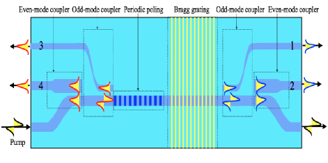
More generally, the deleterious effects of dispersion can be mitigated by mapping every possibility for each available degree of freedom into a different path, resulting in the conversion of modal, spectral, and polarization entanglement into path entanglement.
Consider, as an example, a Type-II interaction. In this case, frequency and polarization are effectively only a single degree of freedom since the photon with frequency above (below) the degenerate value is always (). Thus, two degrees of freedom suffice for characterizing the system: frequency or polarization and mode number. A photonic circuit for converting these two degrees of freedom into photons entangled in path is sketched in Fig. 9. The photons are first separated on the basis of their frequencies, and then on the basis of their mode numbers. Each output port thus carries only a particular degree of freedom, thereby skirting the distinguishability engendered by dispersion-induced time delay. The circuit displayed in Fig. 9 can be viewed as a superposition of those illustrated in Figs. 2 and 6.
The biphoton state entangled in path can be written as
| (15) |
where the subscripts 1, 2, 3, and 4 refer to the output ports labeled in Fig. 9. The photon of frequency is assumed to be back-reflected by the holographic Bragg grating.
In the case of double entanglement, each output port in a circuit such as that shown in Fig. 9 would deliver photons with either TE- or TM-polarization. To avoid distinguishability as a result of polarization-mode dispersion, two methods could be used: 1) each output port could be split into a pair of ports, resulting in eight doubly entangled paths; or 2) an electro-optic TETM mode converter [38] could be used at the path center of each output port, thereby advancing the slow, and retarding the fast, photons in such a way that they would arrive simultaneously at the output detectors.
7 Conclusion
We have presented several photonic-circuit designs based on Ti:LiNbO3 diffused channel waveguides for generating photons with various combinations of modal, spectral, and polarization entanglement. These circuits contain, in various forms, a nonlinear periodically poled two-mode waveguide structure, single- and two-mode waveguide-based couplers, and multiplexed holographic Bragg gratings. Depending on the choice of parameters, the first photonic circuit produces frequency-degenerate down-converted photons with even spatial parity, nondegenerate down-converted photons entangled in frequency, or nondegenerate down-converted photons simultaneously entangled in frequency and polarization. The second photonic circuit produces modal entanglement, or photons that are doubly entangled in mode number and polarization. The third photonic circuit converts modal, spectral, and polarization entanglement into path entanglement to mitigate the effects of dispersion. Simulations have been carried out, with the help of the the commercial photonic and network design software package RSoft, to gauge the performance of these circuits. Furthermore, since Ti:LiNbO3 photonic circuits have the salutary property of permitting the generation, transmission, and processing of photons to be accommodated on a single chip, we expect that they will find use in the efficient implementation of various quantum information processing schemes [14].
References
- [1] C. H. Bennett and G. Brassard, “Quantum cryptography: Public key distribution and coin tossing,” in Proceedings of the International Conference on Computers, Systems & Signal Processing. Bangalore, India: Institute of Electrical and Electronics Engineers, Dec. 1984, pp. 175–179.
- [2] D. N. Klyshko, Photons and Nonlinear Optics. Moscow: Nauka, 1980, Chaps. 1 and 6. Translation: Gordon and Breach, New York, 1988.
- [3] A. Joobeur, B. E. A. Saleh, and M. C. Teich, “Spatiotemporal coherence properties of entangled light beams generated by parametric down-conversion,” Phys. Rev. A, vol. 50, pp. 3349–3361, Oct. 1994.
- [4] A. Joobeur, B. E. A. Saleh, T. S. Larchuk, and M. C. Teich, “Coherence properties of entangled light beams generated by parametric downconversion: Theory and experiment,” Phys. Rev. A, vol. 53, pp. 4360–4371, Jun. 1996.
- [5] B. E. A. Saleh, A. F. Abouraddy, A. V. Sergienko, and M. C. Teich, “Duality between partial coherence and partial entanglement,” Phys. Rev. A, vol. 62, pp. 043 816, Sep. 2000.
- [6] J. G. Rarity and P. R. Tapster, “Experimental violation of Bell’s inequality based on phase and momentum,” Phys. Rev. Lett., vol. 64, pp. 2495–2498, May 1990.
- [7] J. D. Franson, “Inconsistency of local realistic descriptions of two-photon interferometer experiments,” Phys. Rev. A, vol. 61, p. 012105, Dec. 1999.
- [8] A. Mair, A. Vaziri, G. Weihs, and A. Zeilinger, “Entanglement of the orbital angular momentum states of photons,” Nature, vol. 412, pp. 313–316, Jul. 2001.
- [9] S. P. Walborn, S. Pádua, and C. H. Monken, “Conservation and entanglement of Hermite–Gaussian modes in parametric down-conversion,” Phys. Rev. A, vol. 71, pp. 053 812, May 2005.
- [10] A. F. Abouraddy, T. Yarnall, B. E. A. Saleh, and M. C. Teich, “Violation of Bell’s inequality with continuous spatial variables,” Phys. Rev. A, vol. 75, pp. 052 114, May 2007.
- [11] T. Yarnall, A. F. Abouraddy, B. E. A. Saleh, and M. C. Teich, “Experimental violation of Bell’s inequality in spatial-parity space,” Phys. Rev. Lett., vol. 99, pp. 170 408, Oct. 2007.
- [12] ——, “Synthesis and analysis of entangled photonic qubits in spatial-parity space,” Phys. Rev. Lett., vol. 99, pp. 250 502, Dec. 2007.
- [13] M. F. Saleh, B. E. A. Saleh, and M. C. Teich, “Modal, spectral, and polarization entanglement in guided-wave parametric down-conversion,” Phys. Rev. A, vol. 79, pp. 053 842, May 2009.
- [14] M. F. Saleh, G. Di Giuseppe, B. E. A. Saleh, and M. C. Teich, “Modal and polarization qubits in Ti:LiNbO3 photonic circuits for a universal quantum logic gate,” http://arxiv.org/abs/1007.3256. Submitted for publication, Jul. 2010.
- [15] R. Raussendorf and H. J. Briegel, “A one-way quantum computer,” Phys. Rev. Lett., vol. 86, pp. 5188–5191, May 2001.
- [16] E. Knill, R. Laflamme, and G. J. Milburn, “A scheme for efficient quantum computation with linear optics,” Nature, vol. 409, pp. 46–52, Jan. 2001.
- [17] A. Politi, M. J. Cryan, J. G. Rarity, S. Yu, and J. L. O’Brien, “Silica-on-silicon waveguide quantum circuits,” Science, vol. 320, pp. 646–649, May 2008.
- [18] J. C. F. Matthews, A. Politi, A. Stefanov, and J. L. O’Brien, “Manipulation of multiphoton entanglement in waveguide quantum circuits,” Nature Photon., vol. 3, pp. 346–350, Jun. 2009.
- [19] C. H. Bennett and P. W. Shor, “Quantum information theory,” IEEE Trans. Inform. Theory, vol. 44, pp. 2724–2742, Oct. 1998.
- [20] M. A. Nielsen and I. L. Chuang, Quantum Computation and Quantum Information. Cambridge, UK: Cambridge University Press, 2000.
- [21] J. L. O’Brien, A. Furusawa, and J. Vučković, “Photonic quantum technologies,” Nature Photon., vol. 3, pp. 687–695, Dec. 2009.
- [22] A. Politi, J. C. F. Matthews, M. G. Thompson, and J. L. O’Brien, “Integrated quantum photonics,” IEEE J. Sel. Topics Quantum Electron., vol. 15, pp. 1673–1684, Dec. 2009.
- [23] G. Cincotti, “Prospects on planar quantum computing,” J. Lightwave Technol., vol. 27, pp. 5755–5766, Dec. 2009.
- [24] T. D. Ladd, F. Jelezko, R. Laflamme, Y. Nakamura, C. Monroe, and J. L. O’Brien, “Quantum computers,” Nature, vol. 464, pp. 45–53, Mar. 2010.
- [25] M. Fiorentino, S. M. Spillane, R. G. Beausoleil, T. D. Roberts, P. Battle, and M. W. Munro, “Spontaneous parametric down-conversion in periodically poled KTP waveguides and bulk crystals,” Opt. Express, vol. 15, pp. 7479–7488, Jun. 2007.
- [26] M. Avenhaus, M. V. Chekhova, L. A. Krivitsky, G. Leuchs, and C. Silberhorn, “Experimental verification of high spectral entanglement for pulsed waveguided spontaneous parametric down-conversion,” Phys. Rev. A, vol. 79, pp. 043 836, Apr. 2009.
- [27] P. J. Mosley, A. Christ, A. Eckstein, and C. Silberhorn, “Direct measurement of the spatial-spectral structure of waveguided parametric down-conversion,” Phys. Rev. Lett., vol. 103, pp. 233 901, Dec. 2009.
- [28] T. Zhong, F. N. Wong, T. D. Roberts, and P. Battle, “High performance photon-pair source based on a fiber coupled periodically poled KTiOPO4 waveguide,” Opt. Express, vol. 17, pp. 12 019–12 030, Jul. 2009.
- [29] J. Chen, A. J. Pearlman, A. Ling, J. Fan, and A. Migdall, “A versatile waveguide source of photon pairs for chip-scale quantum information processing,” Opt. Express, vol. 17, pp. 6 727–6 740, Apr. 2009.
- [30] S. Tanzilli, H. De Riedmatten, W. Tittel, H. Zbinden, P. Baldi, M. De Micheli, D. B. Ostrowsky, and N. Gisin, “Highly efficient photon-pair source using periodically poled lithium niobate waveguide,” Electron. Lett., vol. 37, pp. 26–28, Jan. 2001.
- [31] M. C. Booth, M. Atatüre, G. Di Giuseppe, B. E. A. Saleh, A. V. Sergienko, and M. C. Teich, “Counterpropagating entangled photons from a waveguide with periodic nonlinearity,” Phys. Rev. A, vol. 66, pp. 023 815, Aug. 2002.
- [32] H. Guillet de Chatellus, A. V. Sergienko, B. E. A. Saleh, M. C. Teich, and G. Di Giuseppe, “Non-collinear and non-degenerate polarization-entangled photon generation via concurrent type-I parametric downconversion in PPLN,” Opt. Express, vol. 14, pp. 10 060–10 072, Oct. 2006.
- [33] H. Nishihara, M. Haruna, and T. Suhara, Optical Integrated Circuits. New York: McGraw–Hill, 1989.
- [34] B. E. A. Saleh and M. C. Teich, Fundamentals of Photonics, 2nd ed. Hoboken, NJ: Wiley, 2007.
- [35] A. C. Busacca, C. L. Sones, R. W. Eason, and S. Mailis, “First-order quasi-phase-matched blue light generation in surface-poled Ti:indiffused lithium niobate waveguides,” Appl. Phys. Lett., vol. 84, pp. 4430–4432, May 2004.
- [36] Y. L. Lee, C. Jung, Y.-C. Noh, M. Park, C. Byeon, D.-K. Ko, and J. Lee, “Channel-selective wavelength conversion and tuning in periodically poled Ti:LiNbO3 waveguides,” Opt. Express, vol. 12, pp. 2649–2655, Jun. 2004.
- [37] R. C. Alferness and R. V. Schmidt, “Tunable optical waveguide directional coupler filter,” Appl. Phys. Lett., vol. 33, pp. 161–163, Jul. 1978.
- [38] R. C. Alferness, “Efficient waveguide electro-optic TETM mode converter/wavelength filter,” Appl. Phys. Lett., vol. 36, pp. 513–515, Apr. 1980.
- [39] J. Hukriede, D. Runde, and D. Kip, “Fabrication and application of holographic Bragg gratings in lithium niobate channel waveguides,” J. Phys. D: Appl. Phys., vol. 36, pp. R1–R16, Jan. 2003.
- [40] D. Runde, S. Brunken, S. Breuer, and D. Kip, “Integrated-optical add/drop multiplexer for DWDM in lithium niobate,” Appl. Phys. B: Lasers Opt., vol. 88, pp. 83–88, Jun. 2007.
- [41] D. Runde, S. Breuer, and D. Kip, “Mode-selective coupler for wavelength multiplexing using LiNbO3:Ti optical waveguides,” Cent. Eur. J. Phys., vol. 6, pp. 588–592, Sep. 2008.
- [42] R. V. Schmidt and H. Kogelnik, “Electro-optically switched coupler with stepped reversal using Ti-diffused LiNbO3 waveguides,” Appl. Phys. Lett., vol. 28, pp. 503–506, May 1976.
- [43] H. Kogelnik and R. V. Schmidt, “Switched directional couplers with alternating ,” IEEE J. Quantum Electron., vol. QE-12, pp. 396–401, Jul. 1976.
- [44] M. M. Fejer, G. A. Magel, D. H. Jundt, and R. L. Byer, “Quasi-phase-matched second harmonic generation: Tuning and tolerances,” IEEE J. Quantum Electron., vol. 28, pp. 2631–2654, Nov. 1992.
- [45] C. K. Hong, Z. Y. Ou, and L. Mandel, “Measurement of subpicosecond time intervals between two photons by interference,” Phys. Rev. Lett., vol. 59, pp. 2044–2046, Nov. 1987.
- [46] R. A. Campos, B. E. A. Saleh, and M. C. Teich, “Fourth-order interference of joint single-photon wave packets in lossless optical systems,” Phys. Rev. A, vol. 42, pp. 4127–4137, Oct. 1990.
- [47] D. H. Jundt, “Temperature-dependent Sellmeier equation for the index of refraction, , in congruent lithium niobate,” Opt. Lett., vol. 22, pp. 1553–1555, Oct. 1997.
- [48] K. K. Wong, Ed., Properties of Lithium Niobate. Stevenage, U.K.: Institution of Electrical Engineers, 2002.
- [49] M. D. Feit, J. A. Fleck, Jr., and L. McCaughan, “Comparison of calculated and measured performance of diffused channel-waveguide couplers,” J. Opt. Soc. Am., vol. 73, pp. 1296–1304, Oct. 1983.
- [50] S. K. Korotky and R. C. Alferness, “Ti:LiNbO3 integrated optic technology,” in Integrated Optical Circuits and Components: Design and Applications, L. D. Hutcheson, Ed. New York: Marcel Dekker, 1987.
- [51] G. B. Hocker and W. K. Burns, “Mode dispersion in diffused channel waveguides by the effective index method,” Appl. Opt., vol. 16, pp. 113–118, Jan. 1977.
- [52] N. Gisin, G. Ribordy, W. Tittel, and H. Zbinden, “Quantum cryptography,” Rev. Mod. Phys., vol. 74, pp. 145–195, Mar. 2002.
- [53] L. E. Myers, R. C. Eckardt, M. M. Fejer, R. L. Byer, W. R. Bosenberg, and J. W. Pierce, “Quasi-phase-matched optical parametric oscillators in bulk periodically poled LiNbO3,” J. Opt. Soc. Am. B, vol. 12, pp. 2102–2116, Nov. 1995.
- [54] R. Ferriere, B.-E. Benkelfat, J. M. Dudley, and K. Ghoumid, “Bragg mirror inscription on LiNbO3 waveguides by index microstructuration,” Appl. Opt., vol. 45, pp. 3553–3560, May 2006.
- [55] A. Norton and C. de Sterke, “Aperiodic 1-dimensional structures for quasi-phase matching,” Opt. Express, vol. 12, pp. 841–846, Mar. 2004.