present address: ]Max-Planck-Institut für Mikrostrukturphysik, Weinberg 2, 06120 Halle, Germany present address: ]Advanced Light Source, Lawrence Berkeley National Laboratory, Berkeley, California 94720, USA
Selective growth of perovskite oxides on SrTiO3 (001) by control of surface reconstructions
Abstract
We report surface reconstruction (RC)-dependent growths of SrTiO3 and SrVO3 on a SrTiO3 (001) surface with two different coexisting surface RCs, namely (21) and c(62). Up to the coverage of several layers, epitaxial growth was forbidden on the c(62) RC under the growth conditions that permitted layer-by-layer epitaxial growth on the (21) RC. Scanning tunneling microscopy on the lattice structure of the c(62) RC revealed that this RC-selective growth mainly originated from the significant structural/stoichiometric dissimilarity between the c(62) RC and the cubic perovskite films. As a result, the formation of SrTiO3 islands was forbidden from the nucleation stage.
pacs:
Valid PACS appear hereThin film engineering via the atomic-scale control of surfaces and interfaces is one of the most important technological assets for regulating and utilizing the functionalities of oxide materials.Ohtomo and Hwang (2004); Brinkman et al. (2007) In particular, SrTiO3 (STO) single crystalline substrates have been widely used to realize low-dimensional oxide structures such as ultrathin filmsChang et al. (2009) and nanowires,Vasco et al. (2005) with properties that are radically different from those of their bulk hosts.
When utilized as a substrate for films composed of other materials, a STO (001) surface terminated with a TiO2 plane and followed by the formation of a (21) reconstruction (RC) constitutes a well-defined surface structure.Chang et al. (2010); Kawasaki et al. (1994); Castell (2002); Erdman et al. (2002) However, slight changes in temperature and/or oxygen partial pressure (PO2) during surface preparation are frequently accompanied by a substantial fraction of other type of RCs.Castell (2002); Jiang and Zegenhagen (1999)
When growing films on STO (001) surfaces, growth mode and rate often change in accordance with the terminations and/or RCs of the substrate surfaces. These growth behaviors have been used to obtain nanometer-sized patterned structures, such as arrangement of molecules,Deak et al. (2006) oxide nanowires,Vasco et al. (2005) and catalytic metal nanoparticles,Silly and Castell (2005) and control their electrical properties. Such self-organized nanostructures show great potential as an alternative, cost-effective, bottom-up approach, but existing microscopic investigations of their physical/chemical growth mechanisms are inadequate.
In this paper, we report scanning tunneling microscopy (STM) observation on the growth behavior of STO and SrVO3 (SVO) films on STO (001) surfaces, on which (21) and c(62)Jiang and Zegenhagen (1999); Lanier et al. (2007) RCs coexist. In contrast to (21) RC, we found that the epitaxial growth of both types of film was prohibited on c(62) RC. Close STM examination on atomic networks of c(62) RC revealed that the perovskite phase was not allowed from the nucleation stage.
Experiments were carried out with an STM system (base pressure 210-10 Torr) combined with a pulsed-laser deposition chamber (base pressure 210-9 Torr). We used Nb(0.1)-doped STO (001) single crystals (CrysTec-GmbH) as substrates. After a NH4F buffered HF treatment, followed by thermal annealing at PO2 = 110-2 Torr and a substrate temperature (Tsub) of 900∘C for about 30 min, in-situ STM and reflection of high energy electron diffraction (RHEED) on the surfaces showed well organized (21) RC terraces separated by STO steps of one unit cell (uc) (0.3905 nm) in height.Kawasaki et al. (1994) To obtain the c(62) RC, we annealed the substrates at Tsub = 950∘C. In order to deposit STO and SVO films, a STO single crystal and a sintered polycrystalline Sr2V2O7 target were ablated at PO2 = 110-4 Torr and Tsub = 600700∘C using a KrF excimer laser ( = 248 nm) with a repetition rate of 1 Hz and an energy density of 3 J/cm2 on the target surfaces.
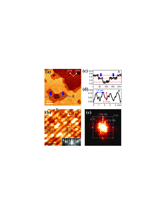
Figure 1 (a) shows the STO (001) substrate surface annealed at PO2 = 110-2 Torr and Tsub = 950∘C for 60 min. The surface exhibits atomically flat terraces. However, the profile along line A, shown in Fig. 1 (c), reveals some regions half a uc ( 0.2 nm) higher/lower than normal terraces of the STO (001). The portion of such regions increased with the longer annealing time.
Figure 1(b) is the atomic resolution STM image of such a region. It clearly shows the stripe patterns running along [100] with the protruding zigzag atomic networks. As shown in Figure 1(d), the profile perpendicular to the stripe patterns (line B) revealed large hill-valley structures. Note that the corrugation of 0.1 nm is larger than the nominal atomic corrugations by the factor of 10, and the stripe patterns clearly showed a periodicity of 1.2 nm which is three times larger than the STO lattice constant. We also confirmed this periodicity by two additional spotsKoster et al. (2000) between the 0th and 1st diffraction peaks in the RHEED pattern, as shown in the inset of Fig. 1(b). Such structures have been identified as the c(62) RC of the STO (001),Jiang and Zegenhagen (1999); Lanier et al. (2007) as the uc is denoted by the rectangular box in Fig. 1(b).
Since STM has been known to image mostly Ti atoms for STO surfaces,Johnston et al. (2007) the characteristic features of the c(62) RCs observed in this study seem to originate from the arrangement of Ti atoms. In addition, a model study on the STO c(62) RC predicted that the incorporations of Ti atoms with different valences in the near-surface TiOx phases can result in zig-zag ordering of truncated Ti octahedras at the center of a stripe and considerable vertical corrugations of the stripe patterns.Lanier et al. (2007) Our observations are consistent with those earlier works.
Figure 1(e) shows the power spectrum of the fast Fourier transform (FFT) of Fig. 1 (b). The (1 0) and (1/6 1/2) spots represent the (11) and c(62) surface structures, respectively. Of greater interest is the existence of substructures, indicated by the black mesh in Fig. 1 (b). This corresponds to the strong (1/2 1/2) spots in Fig. 1 (d), representing c(22) structure.
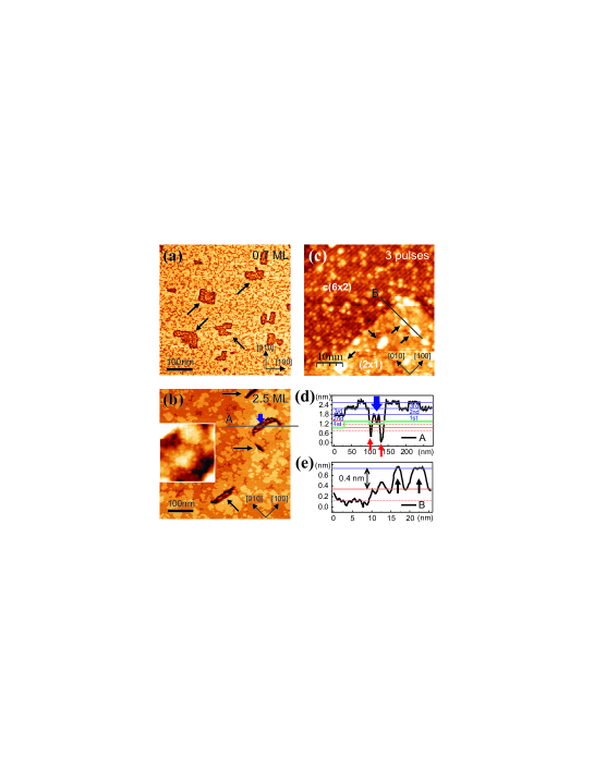
To investigate the growth behavior of the perovskite oxides on this surface of mixed RCs, we deposited a series of STO films, as shown in Figs. 2(a) and (b). Nominal growths followed the layer-by-layer mode. However, we observed disordered structures in some regions, denoted by the black arrows in both images. A magnified STM view (inset of Fig. 2(b))of such a region revealed only the nano-sized grains created by random aggregation of particle-like structures with sizes less than 1 nm. One may infer that those regions were created from the deposition of STO on the c(62) RC by assuming the preservation of the c(62) RC portions on the substrate during growth.
Figure 2 (d) displays the profile along line A in Fig. 2 (b). Aside from the irregular structures, some areas inside the c(62) RC region exhibit STM heights even lower than that of the substrate surface, as indicated by the red arrows. Since the STM height strongly depends on the electronic density of the local position, the observation of such unphysical heights implies that such regions should have different electronic properties from those of the perovskite STO islands.
To understand the microscopic origin of those abnormal growth behaviors, we examined how the island nucleates during the very initial growth stage, realized by extremely small amount of STO influx. We deposited STO by laser ablating the STO target with only three pulses. Figures 2 (c) and (e) show the resulting surface and the height profile, respectively, along the line B. As indicated by the arrows, we observed nucleation of the STO islands, with the well-known 1 uc height of 0.39 nm, in the (21) region. In the c(62) region, however, we could find no such island formation but defective structures of the type shown in Fig. 2 (c). This observation clearly indicates that the island growth was prohibited in the c(62) RC region of STO substrate from the nucleation process.
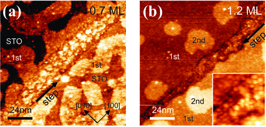
To investigate the role of surface RCs in heteroepitaxial growth, we performed similar experiments on a SVO thin film. Figures 3(a) and (b) show STM images of 0.7 and 1.2 ML SVO films, respectively. The existence of islands with uniform 1-uc heights indicates the layer-by-layer epitaxial growth of the SVO film. In contrast, disordered structures in the regions around the steps can be seen in both images. The inset of Fig. 3 (b) is a magnified view of such a region. The underlying stripes along the [100] direction verify that these regions correspond to c(62) RCs. The SVO films also formed disordered phases on the c(62) RCs of the STO (001) surface, as STO did on similar substrate surfaces.
When c(62) RC and a (001) oriented perovskite film form an interface, free-standing structures of both sides cannot be preserved due to the large lattice mismatch arising from both incommensurate substructure and large vertical deformation of the c(62) RC. Instead, growth could occur with unexpected film orientations: for example, when CdTe film is grown on the STO, the c(62) RC permits the growth of (211) oriented films with the low crystallinity, whereas the substrate of no RC allows the (111) oriented films.Neretina et al. (2009) However, this does not fully explain the growth behaviors of STO and SVO films in our cases, since no crystalline phase with preferred orientation seemed to grow on the c(62) RCs, as observed in the STM images.
Near-surface stoichiometry of c(62) RC could also play an important role of prohibiting the formation of perovskite films by inducing the electrical dissimilarity at the interface. Under harsh preparatory conditions, such as prolonged sputtering and/or high-temperature annealing, it is known that numerous titanium oxide (TiOx) phases and/or nanostructures can be formed on STO (001) surfaces.Deak et al. (2006); Silly and Castell (2004) Therefore, it is quite plausible that the surface layer stoichiometry of the c(62) RC could be extremely different from that of the ideal STO (001) termination.Lanier et al. (2007) Additionally, it is known that the c(62) RC is quite chemically stable in both O2 and the air in spite of structural complexities.Jiang and Zegenhagen (1999) Free-standing (001) STO or SVO surfaces have surface electronic neutrality with uc periodicity. However, the arrangement of the Ti atoms with different valences (see Fig. 1 (b) and description in the text) in the c(62) RC would result in an electrical polarity modulation with a very short periodicity at the interface. This charge modulation could also produce a significant increase in the interface energy.
Therefore, the growth of the perovskite film on c(62) RC, even for that with a low textured orientation, would require large excessive structural deformation and/or stoichiometry changes in the interfacial region.
We demonstrated the significant influence of surface RCs on the initial growth of perovskite epitaxial thin films by using the STO (001) substrate, whose surface were composed of two RCs, (21), c(62). The STM observations revealed that the structural/stoichiometric dissimilarity between the c(62) RCs and the perovskite structure primarily contribute to the selective growth of perovskite films only on (21)RC regions of such substrate. These observations suggest the possibility of applying mixed RC surfaces to the field of oxide heterostructure engineering.
The authors are grateful to M. R. Castell for valuable discussions. This research was supported by the Basic Science Research Program through the National Research Foundation of Korea (NRF) funded by the Ministry of Education, Science and Technology (No. 2009-0080567)
References
- Ohtomo and Hwang (2004) A. Ohtomo and H. Y. Hwang, Nature, 427, 423 (2004).
- Brinkman et al. (2007) A. Brinkman, M. Huijben, M. van Zalk, J. Huijben, U. Zeitler, J. C. Maan, W. G. van der Wiel, G. Rijnders, D. H. A. Blank, and H. Hilgenkamp, Nature Mater., 6, 493 (2007).
- Chang et al. (2009) Y. J. Chang, C. H. Kim, S. H. Phark, Y. S. Kim, J. Yu, and T. W. Noh, Phys. Rev. Lett., 103, 057201 (2009).
- Vasco et al. (2005) E. Vasco, S. Karthauser, R. Dittmann, J. Q. He, C. L. Jia, K. Szot, and R. Waser, Adv. Mater., 17, 281 (2005).
- Chang et al. (2010) Y. J. Chang, A. Bostwick, Y. S. Kim, K. Horn, and E. Rotenberg, Phys. Rev. B, 81, 235109 (2010).
- Kawasaki et al. (1994) M. Kawasaki, K. Takahashi, T. Maeda, R. Tsuchiya, M. Shinohara, O. Ishiyama, T. Yonezawa, M. Yoshimoto, and H. Koinuma, Science, 266, 1540 (1994).
- Castell (2002) M. R. Castell, Surf. Sci., 505, 1 (2002).
- Erdman et al. (2002) N. Erdman, K. R. Poeppelmeier, M. Asta, O. Warschkow, D. E. Ellis, and L. D. Marks, Nature, 419, 55 (2002).
- Jiang and Zegenhagen (1999) Q. Jiang and J. Zegenhagen, Surf. Sci., 425, 343 (1999).
- Deak et al. (2006) D. S. Deak, F. Silly, K. Porfyrakis, and M. R. Castell, J. Am. Chem. Soc., 128, 13976 (2006).
- Silly and Castell (2005) F. Silly and M. R. Castell, Phys. Rev. Lett., 94, 046103 (2005).
- Lanier et al. (2007) C. H. Lanier, A. van de Walle, N. Erdman, E. Landree, O. Warschkow, A. Kazimirov, K. R. Poeppelmeier, J. Zegenhagen, M. Asta, and L. D. Marks, Phys. Rev. B, 76, 045421 (2007).
- Koster et al. (2000) G. Koster, G. Rijnders, D. H. A. Blank, and H. Rogalla, Physica C, 339, 215 (2000).
- Johnston et al. (2007) K. Johnston, M. R. Castell, A. T. Paxton, and M. W. Finnis, Phys. Rev. B, 70, 085415 (2007).
- Neretina et al. (2009) S. Neretina, R. A. Hughes, G. A. Devenyi, N. V. Sochinskii, J. S. Preston, and P. Mascher, Appl. Surf. Sci., 255, 5674 (2009).
- Silly and Castell (2004) F. Silly and M. R. Castell, Appl. Phys. Lett., 85, 3223 (2004).