Optical conductivity and superconductivity in LaSb2
Abstract
We have measured the resistivity, optical conductivity, and magnetic susceptibility of LaSb2 to search for clues as to the cause of the extraordinarily large linear magnetoresistance and to explore the properties of the superconducting state. We find no evidence in the optical conductivity for the formation of a charge density wave state above 20 K despite the highly layered crystal structure. In addition, only small changes to the optical reflectivity with magnetic field are observed indicating that the MR is due to scattering rate, not charge density, variations with field. Although a superconducting ground state was previously reported below a critical temperature of 0.4 K, we observe, at ambient pressure, a fragile superconducting transition with an onset at 2.5 K. In crystalline samples, we find a high degree of variability with a minority of samples displaying a full Meissner fraction below 0.2 K and fluctuations apparent up to 2.5 K. The application of pressure stabilizes the superconducting transition and reduces the anisotropy of the superconducting phase.
1 Introduction
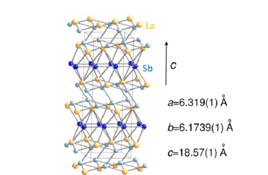
The observation of a large linear magnetoresistance, MR, in the diantimonide, Sb2 (La-Nd, Sm), family of compounds has stimulated recent interest because of the difficulty in modeling such behavior. These materials are layered compounds that crystallize in the orthorhombic SmSb2 crystal structure demonstrated in Fig. 2[1]. This structure is characterized by La/Sb layers that alternate with flat, rectangular, sheets of Sb atoms stacked along the crystallographic c-axis. All of the Sb2 compounds are metallic with LaSb2 reported to be superconducting, SC, with a critical temperature, , of 0.4 K[2] that is not yet fully characterized. For these reasons we investigated LaSb2 to explore the mechanism for the large MR and its SC properties.


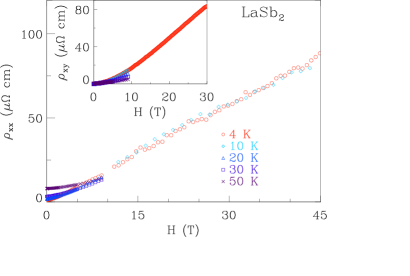
The MR of LaSb2 reproduced in Fig. 2 is linear in field above 3 T[3], is highly anisotropic, and does not saturate in fields of up to 45 T. These features led to the suggestion that LaSb2 is useful as a magnetoresistive sensor for high field applications[4]. Several mechanisms have been proposed over the past 35 years to explain anomalously linear MRs which were observed in disordered semiconductors[5], two-dimensional (2D) heterostructures[6], and elemental metals[7, 8]. The purported causes include the nucleation of charge density wave (CDW) distortions with MR due to quantum fluctuations about the CDW[9] ground state and/or a magnetic breakdown of the CDW gap[10], high field quantization effects[11], or singular scattering mechanisms[12]. While LaSb2 does not appear to be in the extreme quantum limit at the fields of Fig. 2, and there is no indication that conditions are favorable for strongly singular scattering, it remains possible that there is a CDW ordering. This possibility is supported by the fact that NbSe2 and TaSe2, two prototypical CDW systems[13], have similar crystal structures and linear MRs[14, 15]. However, measurements of the resistivity, , showed no transitions or unusual temperature, , dependencies that one usually associates with a CDW transition[3] and photoemission[16] and neutron diffraction measurements[17] did not reveal any phase transitions.
Here, we present optical ellipsometry, reflectivity, , and magnetic susceptibility, , measurements of single crystalline LaSb2. In agreement with the previous measurements outlined above, our optical measurements reveal no features indicative of CDW formation. We find an extraordinarily wide transition to an anisotropic SC phase that sharpens with pressure and which suggests that SC phase fluctuations determine .
2 Experimental details
Single crystals of LaSb2 were grown from high purity La and Sb by metallic flux methods that had typical dimensions 0.5 by 0.5 by 0.02 cm. The crystal structure displayed in Fig. 2 was determined from single crystal x-ray diffraction. Optical experiments were performed using spectroscopic ellipsometry at 0.75 - 3.7 eV in combination with reflectivity measurements from 7 meV to 0.85 meV. Because there is no significant difference between the 300 and 20 K reflectivity spectra in the mid-infrared energy range, the ellipsometry data were obtained at room temperature. All measurements were performed on freshly polished crystals introduced into a vacuum cryostat for the -dependent measurements and kept in a flow of dry nitrogen for room experiments in order to avoid the contamination of the surface. To obtain the absolute value of the reflectivity a reference gold layer was evaporated in situ on the sample surface. From the frequency, , dependent reflectivity and ellipsometry data we derived the real part of the conductivity using a Kramers-Kronig consistent variational fitting procedure[18]. Reflectivity measurements were carried out in s of up to 7 T at a few selected s. ac susceptibility measurements were performed in a commercial SQUID magnetometer down to 1.75 K and in a dilution refrigerator ac probe for mK. Hall effect and measurements were performed on single crystals with electrical contacts made using silver epoxy employing lock-in techniques at 17 or 27 Hz at s between 0.05 and 300 K. Some measurements reported here were made at the National High Magnetic Field Laboratory in continuous fields of up to 45 T (35 T) for (Hall effect) measurements. The crystals studied here had residual ratios of between 70 and 90 for s between 300 and 4 K.
3 Experimental Results
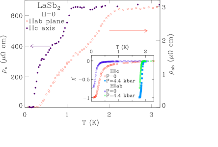
The transverse MR, , and Hall resistivity, , measured with currents parallel to the ab planes presented in Fig. 2 are similar to previous measurements[3, 4] displaying a large, highly linear MR and a large Hall constant. With the Hall carrier density, , estimated to be cm-3 and using the effective mass determined from previous de Haas-van Alphen experiments[19] of times the bare electron mass, we estimate the mean free path, , to be 3.5 m for carriers moving along the ab planes. The resistivity along the c-axis, is up to 200 times larger at 4 K as can be seen in Fig. 4.


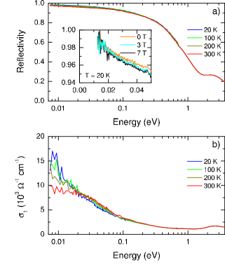
The optical reflectivity spectra of LaSb2 at several s is presented in Fig. 4. All spectra show a typical metallic behavior with a high value of the reflectivity at low and a well defined plasma edge at 1.7 eV. The conductivity, , spectra obtained from the reflectivity and ellipsometry measurements are displayed in Fig. 4b. These data show a small dependence and no interband transition appears to be present at low energy. At higher energy a peak centered at about 2.5 eV is attributed to an interband transition. At low , is featureless and displays no features which can be associated with the opening of a CDW gap. The normalized reflectivity versus photon energy for three applied magnetic fields at K is shown in the inset of Fig. 4a. We see no systematic trends in these data outside of the measurement error as is increased. The data agree with simple estimates of the field induced changes to the reflectivity based upon the MR of Fig. 2 and the Hagen-Rubens formula. Our data rule out any significant change to the electronic structure of LaSb2 with magnetic field at energies above 10 meV.
The wide transition into the SC phase as probed by and ac measurements is displayed in Fig. 4. Both of these quantities show a very wide, anisotropic, phase transition where decreases and the real part of the ac magnetic susceptibility, , inset, displays diamagnetism below 2.5 K. Here is shown for a crystal displaying a complete Meissner fraction, , for ac excitation fields, , along the c-axis for K. The application of moderate pressure, represented in the inset to Fig. 4 by data at 4.4 kbar, significantly sharpens the transition so that by 1.7 K for .
4 Discussion and Conclusions
Our measurements of of LaSb2 effectively rule out the formation of a CDW phase above 20 K showing no unusual changes from a typically metallic form. In addition, we see no significant changes in the reflectivity with magnetic field. Thus, our data suggest that the MR is a scattering induced effect which is not related to the formation of a CDW induced energy gap or variations of the electronic structure with . In addition, our measurements reveal an unusual, anisotropic, SC transition that is very broad in that is incomplete down to our lowest s in the majority of crystals. The application of sharpens the transition dramatically, inducing a full SC transition. Similar SC phase transitions have been previously observed in layered materials such as 2H-TaS2 where the width of the transition was associated with the competition of a CDW phase[20]. In LaSb2 we have found no indication of a CDW, or other energy gap inducing, phases that compete with superconductivity either in above 20 K nor in at any . This suggests a different cause for the wide SC transition we observe. Because the transition sharpens with pressure, and because of the long for charge carriers moving parallel to the ab planes, we do not believe impurity or crystal defects to be important. Instead we suggest that the SC phase in LaSb2 at may be phase fluctuation limited as in the underdoped high SC cuprates.
4.1 Acknowledgments
JFD, DPY, and JYC acknowledge support from the NSF through DMR 084376, 0449022, and 0756281. PWA acknowledges support from the U.S. DOE through DE-FG02-07ER46420. Work at the NHMFL was performed under the auspices of the NSF and the state of Florida.
References
References
- [1] Wang R and Steinfink H 1967 Inorg. Chem. 6 1685
- [2] Hulliger F and Ott H R 1977 J. Less-common met. 55 103
- [3] Bud’ko S L, Canfield P C, Mielke C H and Lacerda A H 1998 Phys. Rev. B 57 13624
- [4] Young D P, Goodrich R G, DiTusa J F, Guo S, Adams P W, Chan J Y and Hall D 2003 Appl. Phys. Lett. 82 3713
- [5] Husmann A, Betts J B, Boebinger G S, Migliori A, Rosenbaum T F and Saboungi L 2002 Nature 417 421
- [6] Stormer H L, Baldwin K W, Pfeiffer L N and West K W (1992) Sol. St. Commun. 84 95
- [7] Falikov L M and Smith H 1972 Phys. Rev. Lett. 29 124
- [8] Kapitza P L 1928 Proc. R. Soc. London, Ser. A 119 358
- [9] Castro Neto A H 2001 Phys. Rev. Lett. 86 4382
- [10] Wilson J A, DiSalvo F J and Mahajan S 1975 Adv. Phys. 24 117
- [11] Abrikosov A A 1999 Phys. Rev. B 60 4231
- [12] Young R A 1968 Phys. Rev. 175 813
- [13] Moncton D E, Axe J D and DiSalvo F J 1975 Phys. Rev. Lett. 34 734
- [14] Morris R C, Coleman R V and Bhandari R 1972 Phys. Rev. B 5 895
- [15] Naito M, Tanaka S and Miura N 1981 Physics in High Magnetic Field edited by Chikazumi S and Miura M (Springer NY) 320.
- [16] Acatrinei A I, Browne D, Losovyi Y, Young D P, Moldovan M, Chan J Y, Sprunger P T and Kurtz R L 2003 J. Phys. Cond. Mat. 15 L511
- [17] Kurtz R L Private communication.
- [18] Kuzmenko A B 2–5 Rev. Sci. Instrum. 76 083108
- [19] Goodrich R G, Browne D A, Kurtz R L, Young D P, DiTusa J F, Adams P W and Hall D (2004) Phys. Rev. B 69 125114
- [20] Nagata S, Aochi T, Abe T, Ebisu S, Hagino T, Seki Y and Tsutsumi K 1992 J. Phys. Chem. Solids 53 1259