Band gap bowing of binary alloys: Experimental results compared to theoretical tight-binding supercell calculations for CdxZn1-xSe
Abstract
Compound semiconductor alloys of the type AxB1-xC find widespread applications as their electronic bulk band gap varies continuously with , and therefore a tayloring of the energy gap is possible by variation of the concentration. We model the electronic properties of such semiconductor alloys by a multiband tight-binding model on a finite ensemble of supercells and determine the band gap of the alloy. This treatment allows for an intrinsic reproduction of band bowing effects as a function of the concentration and is exact in the alloy-induced disorder. In the present paper, we concentrate on bulk CdxZn1-xSe as a well-defined model system and give a careful analysis on the proper choice of the basis set and supercell size, as well as on the necessary number of realizations. The results are compared to experimental results obtained from ellipsometric measurements of CdxZn1-xSe layers prepared by molecular beam epitaxy (MBE) and photoluminescence (PL) measurements on catalytically grown CdxZn1-xSe nanowires reported in the literature.
pacs:
71.15.Ap, 71.20.Nr, 71.23.-k, 73.61.GaI Introduction
For a wide class of compound semiconductor materials AC and BC, alloys of the type AxB1-xC can be realized. These substitutional alloys find a large variety of applications, in particular in nanoelectronic structures like quantum wells, quantum wires and quantum dots. Since the bulk band gap varies continuously with , a tayloring of the energy gap is possible by variation of the concentration. Most of the II-VI and III-V compound semiconductors, e. g. CdSe, ZnSe, CdS, CdTe, GaAs or InAs possess a direct band gap, covering the entire visible spectrum, which makes them particularly suitable in optoelectronic and especially photonic devices.
Many of these materials show a pronounced bowing behaviour of the bulk band gap as a function of the concentration . The deviation from linear behaviour can often be described using a single bowing parameter . The concentration dependent energy gap of the mixed crystal is then given by
| (1) |
where and are the corresponding gaps of the pure AC and BC material. When the pure materials AC and BC have considerably different lattice constants, also a non-parabolic dependence of the band gap on is observed. Richardson and Hill (1973) Nevertheless, a fit of experimental band gap data by the ansatz (1) is still common and adequately possible for materials like CdxZn1-xSe, AlxGa1-xAs, InxGa1-xAs and many more.
The corresponding literature values for the parameter usually show a large variety, depending on the theoretical or experimental approach used. In the present paper we will concentrate on bulk CdxZn1-xSe, where a broad range of values between and eV is reported. Ammar (2001); Venugopal et al. (2006); Tit et al. (2009a); Gupta et al. (1995) From the experimental point of view, this discrepancy considerably originates from the fact that the stable phase of pure CdSe is the wurtzite phase, while pure ZnSe will crystallize in the cubic zincblende modification. Also, the experimental realization has to deal with phase separation effects and the miscibility gap of the alloys. This makes it difficult to grow homogeneously alloyed CdxZn1-xSe bulk samples over the whole concentration range. These problems carry over directly to the theoretical side, as the experimental determination of material properties and hence input parameters for calculations involving zincblende CdSe is very difficult and will often depend on the substrate on which the sample was grown.
In the past, a broad spectrum of different computational methods has been applied to calculate the band gaps of alloyed II-VI and III-V bulk systems, from highly-sophisticated methods like empirical pseudopotential Bernard and Zunger (1986) or DFT + LDA Bernard and Zunger (1987) models, over empirical tight-binding models (ETBM) Tit et al. (2009b, a) to simple two band modelsVechten and Bergstresser (1970). Within the ETBM, one common approach is to use a plane-wave basis set and implicitly map the alloyed and therefore disordered systems onto an effective translationally invariant system by either using a simple linear interpolation of relevant parameters (virtual crystal approximation, VCA) or more sophisticated Green function methods (coherent potential approximation, CPA). Because the VCA is known to vastly underestimate the band gap bowing in most cases, Boykin et al. (2007) and the standard CPA approaches also fail to give quantitatively accurate results, Hass et al. (1983); Laufer and Papaconstantopoulos (1987) tight-binding (TB) methods that use a localized basis set on a finite supercellBoykin and Klimeck (2005) are more promising nowadays. These models, albeit computationally costful, are able to reproduce bowing effects and are exact in the disorder.
To calculate the electronic properties of such semiconductor alloys, we start from multiband tight-binding models for the pure bulk semiconductor materials AC and BC and then perform calculations on a finite ensemble of supercells. We will make recommendations for the cell size as well as for the necessary number of realizations, based on the convergence of the bowing parameter. These recommendations will then be verified by comparison to band gaps as determined from photoluminescence data for catalytically grown CdxZn1-xSe nanowires by Venugopal et al. Venugopal et al. (2006) We also present new experimental results obtained for CdxZn1-xSe films grown by MBE, for which the band gap is determined by an analysis of absorption data. A good agreement between these experimental results and the theoretical results of the TB supercell approach is obtained.
II Theory
II.1 Empirical tight-binding model for pure bulk semiconductors: The effective bond-orbital model
Linear combinations of atomic orbitals can be used as ansatz for the Wannier functions that are localized within the unit cell of the Bravais lattice. From these Wannier functions, the itinerant Bloch functions can be determined by a unitary transformation. Because neither the atomic states nor the Wannier functions are explicitly used in an ETBM, one can directly assume a basis of Wannier-like functions, which is the basic idea of the so-called effective bond-orbital model (EBOM). This resolution on the scale of unit cells is especially convenient for the case of binary semiconductor compounds of the type AxB1-xC, as each unit cell can either be occupied by the AC- or BC-material, respectively.
In order to adequately reproduce one -like conduction band (CB) and three -like valence bands, the heavy hole (HH), light hole (LH) and split-off (SO) band, we use a localized basis per spin direction:
| (2) |
Here labels the sites of the fcc lattice, which is the underlying Bravais lattice of the zincblende crystal structure.
The TB matrix elements of the bulk Hamiltonian are then given by
| (3) |
When restricting the non-vanishing matrix elements, Eq. (3), up to second nearest neighbors, a one-to-one correspondence between the TB matrix elements and a set of material parameters can be determined. In the present work, we use the parametrization scheme of Loehr, Loehr (1994) which fits the bulk band structure to a set of material parameters, namely the bulk band gap , the conduction band effective mass , the spin-orbit splitting , the conventional lattice constant and additionally to the X-point energies of the conduction band , the HH and LH bands (which are degenerate at the Brillouin zone boundary), and the SO band . We use a set of material parameters from Refs. Kim et al., 1994; Hölscher et al., 1985, augmented by -point energies from Ref. Blachnik et al., 1999. This Hamiltonian has already been used succesfully for bulk as well as nanostructure calculations for several material systems. For detailed comparisons with other well-established models, we refer to Refs. Marquardt et al., 2008; Schulz et al., 2009. Our specific choice of values for the material parameters for CdSe and ZnSe has been proven to be reliable in calculations for pure quantum dots Schulz and Czycholl (2005) as well as for mixed CdxZn1-xSe colloidal nanocrystals. Mourad and Czycholl (2010)
II.2 Treatment of alloying in the effective bond-orbital model
The usual approach for translationally invariant systems like pure bulk crystals is the construction of a plane-wave basis set from Eq. (2), which then fulfills the Bloch condition. For the CdxZn1-xSe alloy system, we will now assume uncorrelated substitutional disorder and hence lose the translational symmetry. In analogy to calculations for zero-dimensional nanostructures, Marquardt et al. (2008); Schulz et al. (2009); Mourad et al. (2010) we will use a finite supercell with periodic boundary conditions, with the localized basis, Eq. (2), on each lattice site. Each primitive cell will either be occupied by the diatomic CdSe or ZnSe basis, where the probability for the respective species is directly given by the concentrations and . Accordingly, we will use the matrix elements, Eq. (3) of the pure CdSe or ZnSe material for the corresponding lattice sites and use a linear interpolation for hopping matrix elements between unit cells of different material. Due to the resolution on the Bravais lattice, all influences which stem from effects on a smaller length scale, like the difference in the Cd–Se and Zn–Se bond lengths, are absorbed into the values of the corresponding TB matrix elements between the “effective“ orbitals. Furthermore, we incorporate an appropriate valence band offset (VBO) between the two materials by shifting the respective site-diagonal matrix elements by the value eV, as established in Ref. Schulz and Czycholl, 2005. Although this treatment of the intersite hopping and the VBO has merely been well-proven for interfaces in quantum dot systems, Mourad et al. (2010); Marquardt et al. (2008); Schulz et al. (2009) our results for the bowing have turned out to be insensitive not only to the choice of the interface treatment but also to the specific value of (not shown).

The numerical diagonalization of the corresponding Hamiltonian for each concentration and microscopic configuration gives the density of states (DOS) of the finite ensemble, from which the band gap for each concentration can be determined as the difference between the overall lowest conduction band and highest valence band energy. Fig. 1 shows the corresponding band gap over the concentration in dependence on the number of lattice sites (for fixed number of realizations), where each lattice site corresponds to one unit cell and thus two atoms. Obviously, too small supercells produce an artificially high band gap bowing even with periodic boundary conditions, and this finite size effect cannot be compensated for by a higher number of realizations (not shown here). This could be attributed to clustering effects, as a local accumulation of the small band gap material will lead to an overall smaller band gap from the DOS. Our studies reveal that statistically relevant convergence for the bowing is safely reached with 4000 lattice sites (8000 atoms) and realizations when seeking for a resolution of 10 meV, which corresponds to the last digit of the input energies. With a cubiform supercell, which does not artificially confine the degrees of freedom of the microscopic disorder, this corresponds to an edge length of . Of course, these large supercells and high number of configurations require large computational costs.
From our results, we cautiously conclude that ETBM calculations which use a lesser number of atoms on rectangular supercells (like Ref. Boykin et al., 2007, where an approximate band structure is reconstructed with a supercell, i. e. 1280 atoms) could therefore overestimate the bowing of the alloy band gap. We performed first test calculations for other material systems (e. g. GaxAl1-xN) as well and the convergence criterion of 4000 sites and 50 realizations remained still valid.
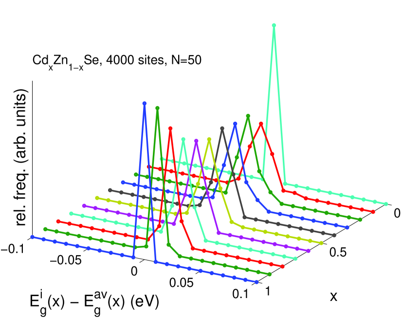
Finally, we want to dicuss the distributions of the band gap values from the different configurations. In theory, the difference between the lowest overall conduction band energy and the highest overall valence band energy corresponds to the band gap of the mixed AxB1-xC crystal, as approximated by the finite ensemble. This is also the usual way to determine band gaps in the CPA, Hass et al. (1983); Laufer and Papaconstantopoulos (1987) which can reproduce broadening effects due to disorder. When referring to the energetic positions obtained from PL peak positions (other effects like the Stokes shift left aside for the moment), one should in principle compare to the ensemble-average of the band gap, because the effects of configurational and concentrational disorder, amongst others, are already absorbed into the finite emission linewidth. is here the difference between the lowest conduction band state and the highest valence band state for the microscopic configuration.
In Fig. 2, we have depicted the relative frequency of the deviation of from the average value for CdxZn1-xSe. As discussed above, we used 50 distinct microscopic configurations and the supercell was chosen to contain 4000 sites in order to reach convergence. The distribution of the is quite narrow for most concentrations and, of course, -like for the pure system ( and ), where all microstates are identical. The biggest deviations, approximately 20 meV, between and occur for . Further studies (not shown) reveal that only the conduction band edge is broadened due to the disorder, while the valence band edge is -like over the whole concentration range within our finite resolution, which is in agreement with CPA calculations for other II-VI alloys. Hass et al. (1983) The overall band gap of the finite ensemble is hence given by
| (4) |
In the present work, we used for the comparison to PL data and the overall band gap of the ensemble DOS for the absorption experiments. Nevertheless, the distributions are so narrow that the bowing parameters calculated in this work only change within the error boundaries when switching between both approaches, provided that the above mentioned convergence criteria are fulfilled.
III Comparison to experimental results
III.1 Comparison to PL on bulk-like nanowires
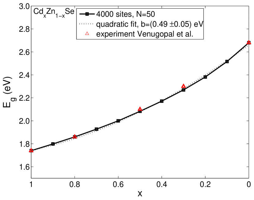
Venugopal et al. performed photoluminescence (PL) and Raman-scattering measurements on catalytically grown CdxZn1-xSe nanowires (60 - 150 nm in diameter and several tens of micrometers in length) in Ref. Venugopal et al., 2006. From these data, they determined the band gap as a function of the concentration and the corresponding bowing parameter. Our TB parameter set was chosen so that their respective experimental band gaps at room temperature for the pure systems, and , are reproduced in our calculations. As opposed to the films discussed in Sec. III.2, the Cd-richer nanowires still tend to crystallize in the wurtzite phase. Regardless, the EBOM results from the localized basis set, Eq. (2), for the band gap will remain valid von Grünberg (1997) when the only slightly larger energy gap of hexagonal CdSe is used in the calculations, especially as the experimental data does not show any discontinuity.
III.2 Comparison to epitaxial films
The samples have been prepared by molecular beam epitaxy (MBE) on a GaAs (100) substrate at a temperature of 280∘C. The binary ZnSe and CdSe layers have been grown directly on the substrate, while for the ternary alloys first a ZnSe buffer layer of 20 nm thickness has been deposited, followed by the CdxZn1-xSe layer. In order to realize different Cd concentrations of the ternary compound, the operating temperature of the Cd Knudsen cell was varied from 226 - 240∘C during deposition. Special care was taken to ensure stoichiometric or slightly Se-rich growth conditions for each case by adjusting the respective flux using both a Se Knudsen cell and a valved cracker source at the same time. A valved cracker source offers the advantage of rapid variations in elemental flux due to the availability of a motorized valve. The stoichiometry has been controlled in-situ employing a reflection high-energy electron-diffraction (RHEED) system. A 21 reconstruction indicates group VI-rich growth, while a c(22) reconstruction can be assigned to metal-rich (i. e. Zn and Cd) conditions. Stoichiometry is achieved when a superposition of both reconstructions can be identified within the RHEED pattern. The growth rate of the CdxZn1-xSe alloy depends sensitively on the II/VI flux ratio. Since the deposition time for CdxZn1-xSe was kept constant (2 hours) for the relevant samples, the thickness of the different CdxZn1-xSe layers show a significant variation. However, this does not influence the accurate determination of the band gap as discussed below.
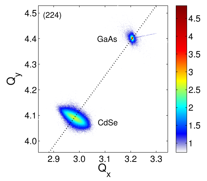
The Cd content and the respective strain state of the CdxZn1-xSe layers has been determined by the evaluation of reciprocal space maps (RSM) in the vicinity of the (224) reflection recorded using high-resolution X-ray diffraction (HRXRD). The RSM measured for the binary CdSe sample () is examplarily shown in Fig. 4. The peak of the CdSe layer is located on a straight line that passes through the origin of the graph, indicating that the layer is fully relaxed and therefore unstrained. The same result is found for the other CdxZn1-xSe films. Merely the layer of the binary ZnSe sample () is not fully relaxed on the GaAs substrate and therefore remains compressively strained. The absence of strain is especially important for the TB modelling for the system under consideration, as it does not have to include the effect of strain and piezoelectricity on the electronic states, as it is often the case in calculations for quantum dot systems. Schulz and Czycholl (2006); Schulz et al. (2008)
In order to evaluate the optical constants, the band gap and the thickness of the CdxZn1-xSe films, optical measurements were carried out using a J. A. Woollam variable-angle spectroscopic ellipsometry (VASE) setup. Aschenbrenner et al. (2010) The spectra cover the wavelength range from 193 nm to 1700 nm (6.42 eV - 0.7 eV) with wavelength steps of 2 nm. To get more accurate data, spectra for three different angles of incidence (65∘, 70∘ and 75∘) were registered and analyzed for each sample. All measurements were perfomed at room temperature. Beside the GaAs (100) substrate, three layers were taken into account, namely the ZnSe buffer, the CdxZn1-xSe-layer and a thin additional layer to include the surface roughness into the model. The latter one was simulated by a Bruggeman effective medium approximation (EMA) using 50% voids in a matrix of the II-VI semiconductor material. The optical constants were derived from the curve fits using a model which combines a Herzinger-Johs “P-semi oscillator” (four connected functions to model each peak)Herzinger and Johs (2010) with four Gauss oscillators.
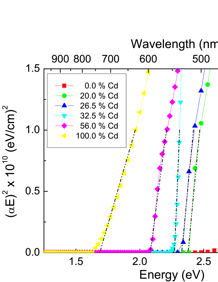
The band gap of the CdxZn1-xSe layers was obtained using the formulaPankove (1975)
| (5) |
and the equation for the attenuation coefficient , where denotes the extinction coefficent, the energy and the wavelength of the incident light. The spectral extinction coefficent is determined by the spectroscopic ellipsometry measurement of the samples and is obtained graphically by evaluating the intersection of the tangent of with the energy axis (see Fig. 5). A comprehensive overview of the relevant experimental parameters for the samples is given in Table 1.
| Cd content (%) | thickness (nm) | roughness (nm) | (eV) |
|---|---|---|---|
| 0.0 | 281.2 | 7.1 | 2.64 |
| 20.0 | 1396.7 | 7.8 | 2.37 |
| 26.5 | 1490.3 | 6.9 | 2.30 |
| 32.5 | 1821.0 | 7.3 | 2.25 |
| 56.0 | 1170.4 | 4.4 | 2.07 |
| 100.0 | 304.0 | 2.6 | 1.69 |
For the theoretical calculations, we determined the TB parameters of the pure systems (i. e. for and ) from standard band structure data in the literature, _cu (2004); Blachnik et al. (1999) valid at room temperature, as the input parameters for the pure cubic CdSe were determined under the same experimental conditions and on the same substrate as in the present measurements.
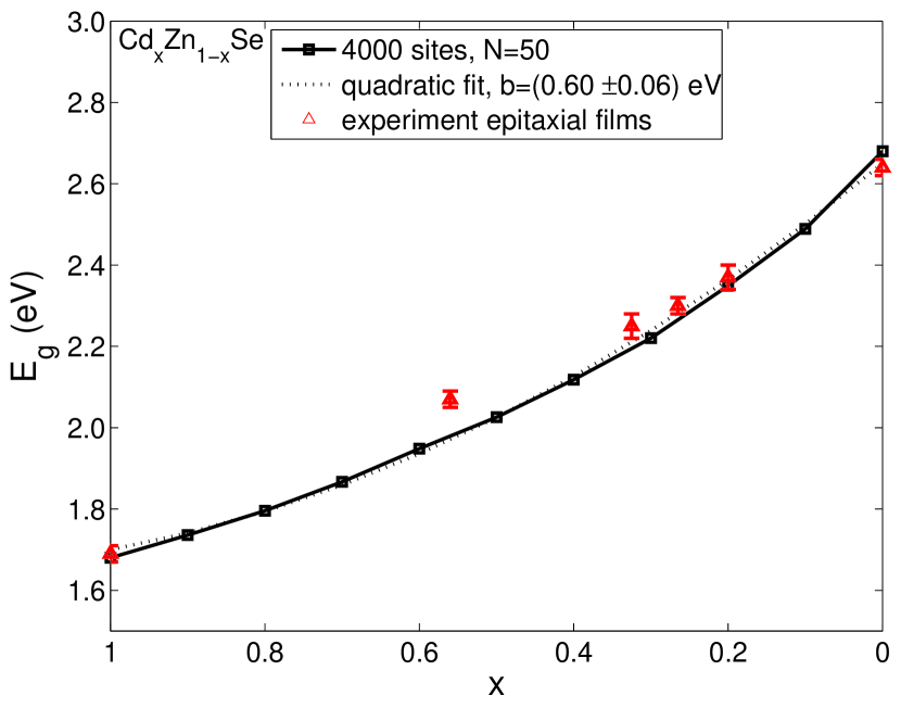
The values for the band gap in dependence on the Cd fraction are depicted in Fig. 6 in comparison with the theoretical results. We get a good agreement within the error boundaries between the experiment and the theoretical data, except for one data point with the concentration , which clearly does not fit the general trend in the data. When this point is omitted, the experimental bowing coefficient is eV, which lies below the theoretical result of eV from the TB calculations for the system under consideration. This discrepancy could for example be explained by the different experimental conditions, as especially the production of high-quality CdxZn1-xSe films, but also the determination of the band gap from the absorption edges may be afflicted with a slightly higher degree of uncertainty than the shift-adjusted PL measurement of the nanowires of Ref. Venugopal et al., 2006. For example, a look at Tab. 1 reveals that the literature value of eV for pure ZnSe at room temperature Blachnik et al. (1999) cannot be exactly reproduced. For the sake of completeness, we would like to note that one obtains an experimental bowing value of eV, which fits the theoretical result within the error range, if the literature value is used for the binary ZnSe sample instead.
III.3 Comparison of the bowing results
For the sake of comparison, the results for the bowing of CdxZn1-xSe for both experiments are summarized in Table 2. In spite of the overall good agreement, the results from the TB supercell calculations for the disordered systems () are all slightly shifted to lower energies in comparison to the experimental values, which result in the higher bowing parameter in the theory.
| system | experiment | supercell ETBM |
|---|---|---|
| nanowires | Venugopal et al. (2006) | |
| epitaxial films |
When we have a closer look at the values for the bowing coefficient , we can conclude that, in spite of the different experimental conditions and therefore boundary values at and , all bowing values lie within the comparatively narrow range between eV and eV. This stands in contrast to several previous studies, who reported a broad variety of values between and eV, Ammar (2001); Venugopal et al. (2006); Tit et al. (2009a); Gupta et al. (1995) as already mentioned in the introduction. Therefore, we recommend a critical review of literature values outside the range given in Tab. 2 before using them for further purposes.
IV Conclusion and outlook
In this paper, we presented a combined theoretical and experimental approach for the determination of the band gap bowing of binary compound semiconductor alloys of the type AxB1-xC. On the theoretical side, we used a multiband empirical tight-binding approach with a localized basis set on the lattice sites of a finite supercell with periodic boundary conditions. By calculating the band gap for each concentration from the density of states of a finite ensemble with different microscopic configurations, our approach is exact in the alloy-induced disorder. The input parameters are a set of material properties of the pure AC or BC system, i. e. for the cases and . Using the example of CdxZn1-xSe, we gave recommandations on the minimal size of the supercell and the minimal necessary number of microscopic configurations in order to determine the band gap bowing coefficient with the same degree of accuracy as the input parameters, as Fig. 1 showed that the results depend strongly on these model parameters.
Furthermore, we compared our results for the band gap bowing of CdxZn1-xSe with two slightly distinct experimental realizations. At first, we compared our results to photoluminescence data from catalytically grown CdxZn1-xSe nanowires by Venugopal et al. Then we used our TB model for an analysis of absorption data from unstrained MBE-grown CdxZn1-xSe films, and also gave a detailed description of the experimental realization of this data set. In both cases, our model fits the experimental data well. For the nanowires PL data, even the experimental band gap bowing parameter can be reproduced within the error margin, while the measurements on the epitaxially grown films show a slightly higher deviation from the theoretical predictions. Nevertheless, within the experimental accuracy the bulk band gaps from all but one MBE samples fit the theoretical curve well. Dependent on the specific experimental conditions, we carefully approve to narrow down the range of the bowing parameter for bulk CdxZn1-xSe at room temperature to between eV and eV.
In contrast to common tight-binding models, which treat the disorder within a mean-field framework, like the virtual crystal approximation, our simple TB supercell approach is able to satisfactorily reproduce the experimental findings and can thus be used to coherently calculate bowing coefficients for other material systems and growth conditions, which in addition may not be experimentally accessible over the whole concentration range. For this purpose, our model can easily be transferred to other material systems like CdxZn1-xS, AlxGa1-xAs, InxGa1-xAs, GaxAl1-xN, and many others in order to calculate the bowing of the band gap. Also, materials with a wurtzite structure can be simulated, as only the corresponding TB Hamiltonian in the effective bond-orbital model has to be replaced by the one given in Ref. Mourad et al., 2010. First results indicate that our minimal criteria for the numerical convergence of the band gap bowing will still remain valid, although this will have to be tested carefully for each system under consideration, in combination with the respective experimental data obtained by means of epitaxy.
Acknowledgements.
The authors would like to thank Jan-Peter Richters and Tobias Voß for fruitful discussions. The financial support of the Deutsche Forschungsgemeinschaft (Project No. 436 RUM 113/27/0-1) is gratefully acknowledged.References
- Richardson and Hill (1973) D. Richardson and R. Hill, J. Phys. C 6, L131 (1973).
- Ammar (2001) A. H. Ammar, Physica B 296, 312 (2001).
- Venugopal et al. (2006) R. Venugopal, P. Lin, and Y. Chen, The J. Phys. Chem. B 110, 11691 (2006).
- Tit et al. (2009a) N. Tit, I. M. Obaidat, and H. Alawadhi, Journal of Alloys and Compounds 481, 340 (2009a).
- Gupta et al. (1995) P. Gupta, B. Maiti, A. B. Maity, S. Chaudhuri, and A. K. Pal, Thin Solid Films 260, 75 (1995).
- Bernard and Zunger (1986) J. E. Bernard and A. Zunger, Phys. Rev. B 34, 5992 (1986).
- Bernard and Zunger (1987) J. E. Bernard and A. Zunger, Phys. Rev. B 36, 3199 (1987).
- Tit et al. (2009b) N. Tit, I. M. Obaidat, and H. Alawadhi, J. Phys. : Condensed Matter 21, 075802 (2009b).
- Vechten and Bergstresser (1970) J. A. V. Vechten and T. K. Bergstresser, Phys. Rev. B 1, 3351 (1970).
- Boykin et al. (2007) T. B. Boykin, N. Kharche, G. Klimeck, and M. Korkusinski, J. Phys. : Condensed Matter 19, 036203 (2007).
- Hass et al. (1983) K. C. Hass, H. Ehrenreich, and B. Velický, Phys. Rev. B 27, 1088 (1983).
- Laufer and Papaconstantopoulos (1987) P. M. Laufer and D. A. Papaconstantopoulos, Phys. Rev. B 35, 9019 (1987).
- Boykin and Klimeck (2005) T. B. Boykin and G. Klimeck, Phys. Rev. B 71, 115215 (2005),.
- Loehr (1994) J. P. Loehr, Phys. Rev. B 50, 5429 (1994).
- Kim et al. (1994) Y. D. Kim, M. V. Klein, S. F. Ren, Y. C. Chang, H. Luo, N. Samarth, and J. K. Furdyna, Phys. Rev. B 49, 7262 (1994).
- Hölscher et al. (1985) H. W. Hölscher, A. Nöthe, and C. Uihlein, Phys. Rev. B 31, 2379 (1985).
- Blachnik et al. (1999) R. Blachnik, J. Chu, R. Galazka, J. Geurts, J. Gutowski, B. Hönerlage, D. Hofmann, J. Kossut, R. Levy, P. Michler, et al., Numerical Data and Functional Relationships in Science and Technology /Zahlenwerte und Funktionen aus Naturwissenschaften und Technik. New Series - … / BD 41 / Part b / Part a (Springer-Verlag Berlin and Heidelberg GmbH & Co. K, 1999), 1st ed.
- Marquardt et al. (2008) O. Marquardt, D. Mourad, S. Schulz, T. Hickel, G. Czycholl, and J. Neugebauer, Phys. Rev. B 78, 235302 (2008).
- Schulz et al. (2009) S. Schulz, D. Mourad, and G. Czycholl, Phys. Rev. B 80, 165405 (2009).
- Schulz and Czycholl (2005) S. Schulz and G. Czycholl, Phys. Rev. B 72, 165317 (2005).
- Mourad and Czycholl (2010) D. Mourad and G. Czycholl, in preparation (2010).
- Mourad et al. (2010) D. Mourad, S. Barthel, and G. Czycholl, Phys. Rev. B 81, 165316 (2010).
- von Grünberg (1997) H. H. von Grünberg, Phys. Rev. B 55, 2293 (1997).
- Schulz and Czycholl (2006) S. Schulz and G. Czycholl, phys. stat. sol. (c) 3, 1675 (2006).
- Schulz et al. (2008) S. Schulz, S. Schumacher, and G. Czycholl, EPJB 64, 51 (2008).
- Aschenbrenner et al. (2010) T. Aschenbrenner, H. Dartsch, C. Kruse, D. Hommel, M. Anastasescu, M. Stoica, M. Gartner, A. Pretorius, A. Rosenauer, and T. Wagner, J. Appl. Phys. , in preparation (2010).
- Herzinger and Johs (2010) C. M. Herzinger and B. Johs, in print (2010).
- Pankove (1975) J. I. Pankove, Optical Processes in Semiconductors (Dover Pubn Inc, 1975), 2nd ed.
- _cu (2004) in Handbook on Physical Properties of Semiconductors (2004), pp. 311–328.