Metallization of Nanofilms in Strong Adiabatic Electric Fields
Abstract
We introduce an effect of metallization of dielectric nanofilms by strong, adiabatically varying electric fields. The metallization causes optical properties of a dielectric film to become similar to those of a plasmonic metal (strong absorption and negative permittivity at low optical frequencies). The is a quantum effect, which is exponentially size-dependent, occurring at fields on the order of and pulse durations ranging from fs to ns for film thickness nm.
pacs:
73.20.Mf 77.22.Jp 42.65.Re, 72.20.Ht
Effects of strong electric fields on electron states in crystals have attracted a great deal of attention over many decades going back to Zener who predicted breakdown due to interband tunneling Zener (1934). In insulators this requires electric fields on the order of atomic fields V/Å. Interest to strong-field condensed matter physics has recently greatly increased due to the availability of such strong electric fields in laser pulses of intensities . Ultrashort laser pulses with a few optical oscillations Corkum and Krausz (2007); Krausz and Ivanov (2009) open up a possibility to study ultrastrong field phenomena in solids during periods of time too short for the lattice ions to move significantly. Recent ab initio calculations Otobe et al. (2008) have reproduced the Zener breakdown in insulators induced by a laser pulse of intensity . Other strong-field phenomena that can be observable in crystals at a comparable field strength are the appearance of localized electron states, Wannier-Stark ladder in the energy spectrum Wannier (1960); Shockley (1972), and Bloch oscillations. Bloch (1929) At orders of magnitude lower intensities, low-frequency optical fields cause a reduction of the band gap in semiconductors and insulators (Franz-Keldysh effect, FKE) Franz (1958); Keldysh (1958). The quantum confined FKE takes place in semiconductor quantum wells and is determined not by the field but by the total potential drop. Miller et al. (1986) It requires typical fields .
In this Letter we introduce an effect of metallization in insulator nanofilms, which is predicted to occur in applied electric fields . It is based on adiabatic electron transfer in space across the nanofilm. The minimum duration of the field pulse required for the adiabaticity exponentially depends on the crystal thickness varying from fs for a 3 nm film to ns for a 10 nm film thickness. This metallization effect manifests itself by a dramatic change in the optical properties of the system, which start to remind those of metals. In particular, plasmonic phenomena emerge.
To demonstrate the metallization effect, we need to solve the one-electron Schrödinger equation for a periodic potential plus a uniform electric field very accurately. We will employ the widely used Kronig-Penney model for electrons in a film confined in the direction by an infinite potential well. The corresponding potential energy (neglecting the electron-electron interaction) is
| (1) |
where , and is the lattice constant. Crystal thickness is determined by the number of the lattice periods in the direction, . Though this model does not precisely correspond to any real system, it is exactly solvable and catches the qualitative features of the strong-field phenomena from formation of the quantum bouncer (QB) states to band gap collapse and metallization transition. We use the transfer matrix to find an exact solution of the Schrödinger equation with potential (1) – see Sec. II of Supplemental MaterialEPA (2010). The zero boundary conditions for the wave function at have been imposed and energies found semi-analytically using the shooting method.
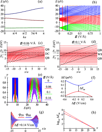
The energy bands of the infinite crystal in the zero field are shown in Fig. 1 (a) by color coded lines for the three lowest bands: localized (green), valence (red), and conduction (blue). The discrete electronic levels for the film in zero field are represented by the black dots superimposed on these infinite-crystal dispersion curves. Our computations are made for and to result in the gap between the conduction and valence bands to be , which is the same as for . We consider an insulator (semiconductor) film where the localized and valence bands are completely filled, and the conduction band is empty. This corresponds to a population of 16 electrons per unit cell (taking spin into account) and a reasonable electron density of .
The energy spectrum of the nanofilm as a function of the applied field normal to the film is shown in Fig. 1 (b) where the filled bands are coded by the green (localized band) and red (valence band), and the empty conduction band is indicated by blue. With an increase of , the linear Stark effect takes place, and the conduction-valence band gap decreases, completely closing at a metallization field indicated by the vertical dashed line. This behavior can be understood from analytical theory presented in Sec. V of the Supplemental MaterialEPA (2010), where Eq. (38) expresses as
| (2) |
Here an electric-field quantum confinement length is , where are the effective masses for electrons and holes, and and are the first roots of and , respectively.
The band gap can be estimated as . From this, we can estimate . Neglecting in comparison with , one obtains a very good approximation for , band edges (where and stand for the top and bottom), and band gap as
| (3) |
This implies a linear Stark effect near the metallization point, in an excellent agreement with Fig. 1 (b).
An applied normal electric field causes the appearance of states localized between the corresponding boundary at and the stopping points whose coordinates and energy are related as [cf. Eqs. (29) and (33) of the Supplemental MaterialEPA (2010)]. These relations are represented by the slanted black lines in Figs. 1 (c) and (d). Carriers at the conduction band bottom behave as electrons, and those at the top of the valence band behave as holes. The corresponding mobility edges are denoted as and . For moderate fields [panel (c)], the states with energies or are Bloch-electron quantum bouncers (QBs) Goodmanson (2000). The states with intermediate energies do not have stopping points and are delocalized, conducting (DC).
For a stronger electric field, as shown in Fig. 1 (d), the mobility edges overlap, , and the DC states disappear. Instead, localized Wannier-Stark (WS) states appear with energies . These states are very close to those in infinite lattices. Shockley (1972) Their contribution to the static conductivity vanishes – see the next paragraph.
Assume that the barriers at the boundaries of the nanofilm are transparent enough to allow for tunneling through. Then it is physically meaningful to find the transmission coefficient for carriers injected at a certain energy, which is plotted in Fig. 1 (e) for the valence and conduction bands for different values of . As increases, the transmission band collapses along with the disappearance of the delocalized conducting (DC) states.
Metallic behavior is actually characterized by two different phenomena: dc conductivity and negative (where is permittivity) that contributes to plasmonic phenomena. They do not necessarily both take place simultaneously. We have shown above that the field-induced localization eliminates the dc conductivity.
Now we will show that, to the opposite, the applied field that increases slowly (adiabatically) turns an insulator crystal into a metal optically, which we call the metallization effect. A distinct property of metals is the absence of a band gap around the Fermi energy. The two levels at the edges of the valence and conduction band at field experience an anticrossing as Fig. 1 (f) shows. The band gap is very small, , which stems from a very little overlap between the wave functions of the two edge state QBs [Fig. 1 (g)].
The minimum splitting of these anticrossing levels is related to the matrix element of the Zener-type tunneling between the valence and conduction bands. This splitting can be calculated analytically using the quasiclassical approximation of Refs. Kane, 1959; McAfee et al., 1951; Glutsch, 2004 and Eq. (3). We obtain
| (4) | |||||
| (5) |
where the reduced mass is .
The dependence of the minimum band splitting on from Eq. (4), where the critical field is given by Eq. (2), is shown in Fig. 1 (h) with a solid red line. It is in an excellent agreement with numerically computed points obtained from our quantum-mechanical solution, which are displayed as bold dots. Dependence given by a simplified expression (5) is shown by the dash blue line in Fig. 1 (h) and is a good approximation.
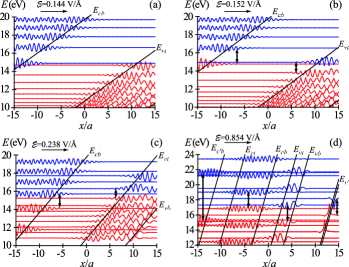
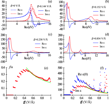
Now we turn to the metallization. Consider first field , which is slightly less than . The corresponding energy levels near the Fermi energy eV are shown in Fig. 2 (a). We assume temperature to be sufficiently low so only the states below are occupied (shown by red) and those with are vacant (blue color). The valence band states are QBs at the right boundary, and those of the conduction band are QBs at the left boundary. Though the band gap is very small, the low-frequency transitions between these two bands are drastically suppressed due to the very weak spatial overlap. This agrees with the corresponding optical spectra for shown in Fig. 3 (a), which are almost the same as for .


Assume that the field is slowly increased to , so that the level anticrossing shown in Fig. 1 (f) is adiabatically passed, which requires that the passage time (cf. Landau-Zener theory Zener (1932)). This necessitates that the nanofilm is thin enough – cf. Eq. (5). Then the passage is adiabatic, the system persists in the ground state, and the electron population remains below the Fermi surface – see Fig. 2 (b). At each boundary of the film, there are QBs on the opposite sides of the Fermi surface, which significantly overlap in space. This allows for strong electron transitions at low frequencies as shown by the vertical double arrows. Note that the transition probability between two QBs rapidly decreases with the transition frequency [see Eqs. (30) and (34) of Supplementary MaterialEPA (2010)]. Correspondingly, the optical absorption is dramatically shifted to the red and infrared (ir) parts of the spectrum as displayed in Fig. 3 (b). In the red spectral region, , which is characteristic of metals. This is the metallization effect.
With a further adiabatic increase of the field to , more levels cross the Fermi surface – see Fig. 2 (c). A stronger low-frequency absorption takes place [Fig. 3 (c)]. This signifies a more developed metallization.
For a very strong field case illustrated in Fig. 2 (d), the Fermi surface separates levels originating from four initial energy bands. The dominating transitions are those between WS states, and their frequency is increasing linearly with . This leads to a general shift of the optical spectra to the blue – see Fig. 3 (d) where the absorption maximum is now at approximately 2 eV.
To emphasize the metallization transition, we show in Fig. 3 (e) the oscillator strength of the low frequency (below 3 eV) transitions as a function of . Note that is characteristic of metals. This figure demonstrates a resemblance between the metallization and a quantum phase transition. Up to the metallization critical field , the oscillator strength is practically zero. After that, increases in steps, each corresponding to a pair of QBs adiabatically crossing the Fermi surface. At the maximum, implying that of the total number of electrons contributes to this metallic behavior. A further increase of leads to the WS states crossing the Fermi surface and the oscillator strength decreasing [cf. Eq. (46) of the Supplemental MaterialEPA (2010)] as shown by the solid green line.
Behavior of the permittivity across the metallization transition is displayed in Fig. 3 (f). Below , is relatively low. For , both and increase in steps due to the QB states crossing the Fermi surface. After reaching the maximum, the main contribution to shifts to the transitions between WS states originating from the same band (either valence or conduction). This causes decrease in as shown by the green and orange lines computed using Eqs. (47)-(48) of the Supplemental MaterialEPA (2010). As field increases, there are also transitions between the WS states originating from the different bands, leading to the sharp peaks in Fig. 3 (f).
Concluding (see also Sec. VIII of Supplemental MaterialEPA (2010)), we have predicted an effect of metallization in dielectric nanofilms induced by an adiabatically increasing applied field. The localized states crossing the Fermi surface cause optical absorption extending from very low (THz) frequencies over all optical region. In the near-ir and red spectral region, is predicted. This property is characteristic of metals and allow for a multitude of nanoplasmonic effects. The metallization cardinally differs from the Zener breakdown in bulk crystals, which is clear from much lower fields required ( for nm). In fact, the metallization is defined not by the field per se but by the total potential difference . Due to the requirement of adiabatic passage to the metallized state, the rise time of the applied electric field exponentially increases with . For instance, for the considered case ( nm, eV), ns, while for nm the passage is much faster: fs.
The manifestations of the metallization depend on the way the field is induced in the nanostructure. For the excitation by an optical or THz wave electric field, the metallization will cause high values of the permittivity and, consequently, bring about the plasmonic behavior of the system. This will lead, in particular, to screening of the external fields limiting the internal fields to . Note that corresponds to the wave intensity , which is well tolerated by nanostructured plasmonic metals – cf. Ref. Kim et al., 2008. In this case, the metallization effect is completely reversible. This will open up the field of nanoplasmonics to a variety of new dielectric and semiconductor nanosystems with a plethora of new phenomena possible. Among potential applications, is an ultrafast field-effect transistor where an ir or optical fs pulse controls a dielectric gate.
In contrast, for dc- to microwave-frequency potential applied via electrodes, the external potential difference is fixed. Then the metallization will lead to and is a new mechanism of the dielectric breakdown, which is fundamentally different from both the Zener and avalanche mechanisms. Such a situation is characteristic for the nanometric layers of the insulator in field-effect transistors and super-capacitors, with far-ranging technological ramifications for microelectronics and energy storage.
We appreciate discussions with F. Krausz and R. Ernstorfer. This work was supported by grants from the Chemical Sciences, Biosciences and Geosciences Division of the BES Office of the US Department of Energy, a grant CHE-0507147 from NSF, and the US-Israel BSF.
References
- Zener (1934) C. Zener, Proc. Royal Soc. A 145, 523 (1934).
- Corkum and Krausz (2007) P. B. Corkum and F. Krausz, Nature Physics 3, 381 (2007).
- Krausz and Ivanov (2009) F. Krausz and M. Ivanov, Rev. Mod. Phys. 81, 163 (2009).
- Otobe et al. (2008) T. Otobe, M. Yamagiwa, J. I. Iwata, K. Yabana, T. Nakatsukasa, and G. F. Bertsch, Phys. Rev. B 77, 165104 (2008).
- Wannier (1960) G. H. Wannier, Phys. Rev. 117, 432 (1960).
- Shockley (1972) W. Shockley, Phys. Rev. Lett. 28, 349 (1972).
- Bloch (1929) F. Bloch, Z. Phys. A 52, 555 (1929).
- Franz (1958) W. Franz, Z. Naturforschung A 13, 484 (1958).
- Keldysh (1958) L. Keldysh, J. Experimentl. Theor. Phys. 34, 5, 1138-1141 (1958); Translation: Sov. Phys. JETP 7, 788 (1958).
- Miller et al. (1986) D. A. B. Miller, D. S. Chemla, and S. Schmitt-Rink, Phys. Rev. B 33, 6976 (1986).
- EPA (2010) See supplementary material at arxiv.org/abs/1007.2366 (2010).
- Goodmanson (2000) D. M. Goodmanson, Am. J. Phys. 68, 866 (2000).
- Kane (1959) E. O. Kane, J. Phys. Chem. Solids 12, 181 (1959).
- McAfee et al. (1951) K. B. McAfee, E. J. Ryder, W. Shockley, and M. Sparks, Phys. Rev. 83, 650 (1951).
- Glutsch (2004) S. Glutsch, Phys. Rev. B 69, 235317 (2004).
- Zener (1932) C. Zener, Proc. Royal Soc. A 137, 696 (1932).
- Kim et al. (2008) S. Kim, J. H. Jin, Y. J. Kim, I. Y. Park, Y. Kim, and S. W. Kim, Nature 453, 757 (2008).