Direct observation of non-equilibrium spin population in quasi-one-dimensional nanostructures
Abstract
Observation of the interplay between interacting energy levels of two spin species is limited by the difficulties in continuously tracking energy levels, and thus leaves spin transport in quantum wires still not well understood. We present a dc conductance feature in the non-equilibrium transport regime, a direct indication that the first one-dimensional subband is filled mostly by one spin species only. How this anomalous spin population changes with magnetic field and source-drain bias is directly measured. We show the source-drain bias changes spin polarisation in semiconductor nanowires, providing a fully electrical method for the creation and manipulation of spin polarization as well as spin-polarized currents.
Quantum dynamics of spins has recently been of central interest for a possible technology of spintronics, the main challenge of which is to generate, manipulate, and detect spin-polarised currents in nanostructures Wolf_science01 ; Zutic_RMP04 . Realization of this technology principally relies on ferromagnetic contacts Jedema_Nature01 ; Urech_NL06 , but efficient spin injection as well as the manipulation of the injected spins remains a challenge for practical applications. Other approaches such as the spin Hall effect Kato_Science04 ; Valenzuela_Nature06 and voltage-induced changes in magnetisation Eerenstein_Nature06 ; Maruyama_NatureNanotech09 have thus been proposed and have attracted considerable interest. Here we directly demonstrate that quasi-one-dimensional (quasi-1D) mesoscopic devices, nanowires and quantum point contacts, can form the basis of a fully electrical method for the creation and manipulation of spin polarisation as well as spin-polarised currents without high magnetic fields or ferromagnetic injecting contacts.
Semiconductor nanowires and quantum point contacts Thornton ; Berggren86 ; vanWees88 are among the simplest mesoscopic devices and have significant applications in quantum information processing as charge sensors Field93 ; Petta_Science05 ; Fujisawa_Science06 . Possible spontaneous spin polarisation, as manifest in the so-called 0.7 anomaly Thomas96 , was suggested to occur in this strongly correlated quasi-1D system and continues to attract fundamental interest within the equilibrium (ohmic) transport regime. Recently, a robust conductance feature at in the non-equilibrium transport regime was linked to a pure spin-polarised current Chen_APL08 , which is a possible candidate for efficient spin injection and detection.
The study of the underlying mechanism of these puzzling conductance features in quasi-1D devices and any associated spin polarisation is severely limited by the difficulties in tracking the quasi-1D subbands, where and are the total densities in each of the two spin bands. Electron transport is frequently studied by measuring the differential conductance when a small ac signal of a few microvolts is applied. However, the differential conductance only provides information on the transport properties at a specific value of the chemical potential, detecting the 1D energy level when it moves across a chemical potential and exhibits a change in value, not elsewhere, as remains unchanged, forming a quantised plateau. Measurement of is also performed in the non-equilibrium transport regime, where a relatively large source-drain dc bias comparable to the subband energy spacings (i.e., a few millivolts) is applied to split the chemical potential into two separate source () and drain potentials (), allowing observation of a subband crossing the source and drain chemical potentials only.
A recently developed method of analysis, the dc conductance of the nanowire , provides a means to track the subband energy level as it is continuously filled by electrons, consequently giving new insights into the conductance anomalies and electron-electron interactions Chen_APL08 ; Chen_PRB09 . The dc conductance — equivalent to an integration of ac conductance — of a single spinless subband is given by , where is the energy separation of and the bottom of the subband when the subband energy lies between two potentials Chen_APL08 . Hence, the subband filling can be directly tracked during the experiment by measuring ; it is being able to follow subband movements which gives the technique its usefulness.
In other words, the dc conductance is the integral of information given by the ac conductances over the range of , which measures the subband filling energy. Such energy-related information cannot be seen in the traces of . In the non-equilibrium regime indicates filling energy and behaves very differently from its corresponding , whereas in the equilibrium regime (as ) there is little difference between them.
In this letter, we describe dc conductance measurements in the non-equilibrium transport region, and present a dc conductance anomaly belonging to the 0.7 family. This anomaly directly demonstrates an unusual spin population behaviour of the quasi-1D subbands, viz., the minority spin-up subband almost stops being filled as carrier density increases with split-gate voltage . This behaviour was previously suggested Lassl ; Abi_PRB07 , but has not yet been directly observed. How it changes with source-drain bias in the non-equilibrium regime is even much less understood. We now demonstrate how this anomalous subband filling changes as a function of magnetic field and source-drain bias, and provide insight into the puzzling conductance anomaly at Thomas_Phil98 ; Kristensen_PRB00 . In addition, we show that the source-drain bias changes the spin polarisation of electrons moving through the quasi-1D devices. The spin-polarised state in the non-equilibrium region is more robust than that in the equilibrium region, and is thus more practical for spintronics. Although the underlying physics is still not understood, we now have a technical ability to electrically generate, manipulate, and detect spin polarisation as well as spin-polarised currents.
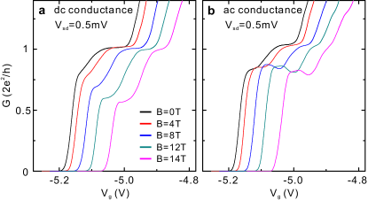
Figure 1(a) and (b) respectively show and versus at mV for in-plane magnetic fields T. A shoulder-like feature of is found at , evolving into a well-defined plateau with increasing magnetic field—the dc conductance value of which drops to at T. In contrast, the corresponding , as shown in Figure 1(b), exhibits a plateau around that barely changes with increasing magnetic field.
The magnetic field induced evolution of the shoulder-like feature in to an almost fully spin polarised state implies that this dc conductance anomaly belongs to the 0.7 family. It is important to note that the source-drain bias alters the spin polarisation. Although both the shoulder-like features in and the 0.7 structure in the equilibrium regime are observed to evolve into a fully spin-polarised plateau with increasing magnetic field, the evolution of each of them is slightly different. The dc conductance value of the plateau at T is still larger than the , showing it is still partially spin-polarised (i.e., ), whereas the 0.7 structure at has already evolved into a fully spin-polarised plateau () at T (not shown).
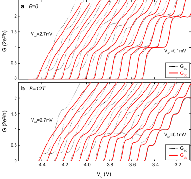
Figure 2(a) shows this feature at incremental values of source-drain bias . and are both quantised in multiples of at low . At a source-drain bias greater than the energy of the subband spacing, there is always at least one subband energy lying between and , resulting in the absence of quantised plateaux in , whereas quantised features in still occur. In addition, it was found that a shoulder-like feature in forms just when evolves into the plateau. Figure 2(b) furthermore shows that these anomalies become more pronounced at T, particularly a non-quantised plateau rising from to , going from low to high dc bias. The anomaly is present for both and T, indicating a zero magnetic field spin polarisation.
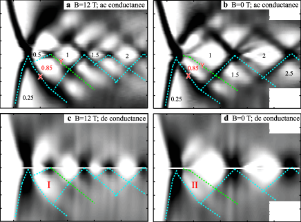
The derivatives of the dc and ac conductance shown in grayscale plots as a function of and [Figure 3] give a clearer picture of the behaviour of and the corresponding . Black indicates areas of high transconductance, such that the branches in the grayscale plot of [Figure 3(a) and (b)] represent a subband edge just passing through a chemical potential, whereas plateaux are white regions. Dotted lines following these branches are drawn schematically in both and grayscale plots in order to illustrate the configuration of the subband levels and the source and drain potentials in various regions.
At T when the spin degeneracy is clearly lifted, the plateau lies in the region in which the spin-down subband has passed through at line X, whilst the spin-up subband lies between and , and passes through at line Y, which separates the region from the plateau, shown in Figure 3(a). As the magnetic field is decreased, line X and line Y gradually move closer to each other, but they do not merge with each other even at [Figure 3(b)]; meanwhile, the plateau itself barely changes with magnetic field. We therefore conclude that the first 1D subband is spin-split even at in the plateau region, where the spin-up subband lies between and , together with the spin-down subband below .
Because measurements of as a function of indicate how electrons between and continuously populate the subband as the 1D channel widens with split-gate voltage, forms a plateau only after the subband moves below both chemical potentials, very different from which forms a plateau whenever the subband energy level is not near a chemical potential. The grayscale plots of [Figure 3(c) and (d)] clearly show that, as expected, plateaux occur when there are no 1D subbands lying between two chemical potentials, such as the regions in which the corresponding exhibits the and the plateau. No plateau is expected in whenever a subband lies between and (i.e., the region between a pair of V-shaped branches) even though the corresponding does exhibit a plateau, for example, the regions of the , the , and the plateau in Figure 3(d). There is, however, an exception for the region where the plateau is found: a dc conductance plateau occurs when the first spin-up subband still lies between and , implying an unusual population behaviour of this subband.
The 0.7-like dc conductance anomaly in the non-equilibrium regime is a direct indication that the first spin-up subband almost stops populating as the carrier density increases with split-gate voltage, since the value of the dc conductance is equivalent to the subband filling . In other words, a plateau or shoulder-like feature in as a function of indicates a slower rate at which electrons fill the subband when it is between and . This implies that the 0.7 structure itself is caused by a similar behaviour of a spin-up subband as , in agreement with the theoretical prediction Lassl and the phenomenological models Bruus ; Reilly . Note that the densities of the two spin types as well as the spin polarisation can be obtained provided that the filling energies in each of the two spin subbands are measured.
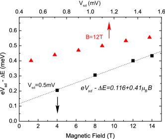
The conductance value of the anomaly decreases with increasing magnetic field [Figure 1(a)] on the one hand, and increases with increasing source-drain bias [Figure 2(b)] on the other. This can be further investigated by calculating from the value of . Figure 4 shows the energy difference between the edge of the first spin-up subband and , i.e., , as a function of (i) magnetic field at mV (black symbols at the bottom), and (ii) source-drain bias at T (red symbols at the top). The points are obtained from the dc conductance value of the anomalous plateau, indicating the energy of the first spin-up level with respect to as it stops populating. This energy gap increases linearly with and follows the relation , where and are two fitting parameters. The linear-least-square fit gives meV and . The parameter is the energy gap at , and is quite close to the effective g-factor of bulk GaAs, , for the Zeeman splitting. The consistency between them implies that the spin-up subband stops populating further, for a range of gate voltages, just when the first spin-down channel with its energy level near is open to electrons moving from the drain. It is important to stress that the nonzero is equal to the spin gap at .
The bias dependence of the energy gap at the top of Figure 4 suggests the same physics. The energy gap, , varying from to meV for source-drain biases between mV and mV at T, is close to the spin-split energy gap, meV, which is obtained using source-drain bias spectroscopy. Note that the energy gap slightly increases with increasing , indicating that it is caused by a combination of Coulomb and exchange interactions. There are proposals that this is expected to widen with increasing carrier density wang96 ; Berggren02 ; Lassl ; Reilly and in our case this corresponds to increasing in the plateau region.
In the plateau region a conductance value of is expected rather than the obtained , although the measured is in general between and . It has been suggested that this anomalous differential conductance value is due to the spin-up subband level being close to and consequently filled in part Kristensen_PRB00 . However, here we have directly measured the subband energy via the dc conductance and found that the subband edge is in fact far above . The plateau behaves in a very different manner from the 0.7 structure, in that it barely changes with temperature up to K, which indicates that it is not significantly affected by thermal broadening and so the 1D subband edges are not close to the chemical potentials.
A nonlinear electron filling of the spin-up subband as a function of could be responsible for the enhancement of differential conductance of the “0.85 plateau”. In a non-interacting model for establishing unidirectional dynamics Glazman ; martinmoreno , the 1D energy level moves linearly with increasing , resulting in a quantised of for a spinless 1D mode. In contrast, any extra population of electrons, caused by the 1D energy level moving downward instead of being fixed with respect to as is increased, will enhance the differential conductance. This model is consistent with the spin population behaviour observed via the dc conductance anomaly. We note that the 0.85 plateau is observed at in InGaAs PSimmonds , implying the significance of the interaction effect in these two systems is different.
To summarize, an anomalous dc conductance feature has been directly related to a non-equilibrium spin population behaviour. This also gives rise to the corresponding differential conductance finite-bias feature at around . We have investigated this dc conductance anomaly and have shown how the population of the minority up-spins and the spontaneous spin polarisation changes as a function of magnetic field and source-drain bias. This provides a key to a more complete understanding of Coulomb and exchange interactions and the 0.7 anomaly in quasi-one-dimensional systems, as well as a fully electrical method for creation and manipulation of spin-polarised currents.
Acknowledgements
We thank useful discussion with F. Sfigakis and L. W. Smith. This work was supported by EPSRC, U.K.
Methods
This work utilized GaAs/Al0.33Ga0.67As heterostructure in which the two-dimensional electron gas is 96 nm below the surface, with a low temperature mobility of cm2/Vs and a carrier density of cm-2. Split-gate devices with a width of 0.8 m and lengths from 0.3 m to 1 m were fabricated and measured and all exhibited similar characteristics. Measurements of differential conductance via the variation of due to a small ac excitation voltage of V, and dc conductance via a larger source-drain dc bias () were performed simultaneously in a dilution refrigerator.
References
- (1) Wolf, S. A., Awschalom, D. D., Buhrman, R. A., Daughton, J. M., von Molnar, S., Roukes, M. L., Chtchelkanova, A. Y., Treger, D. M. Science 294, 1488-1495 (2001).
- (2) Zutic, I., Fabian, J. & Das Sarma, S. Rev. Mod. Phys. 76, 323-410 (2004).
- (3) Jedema, F. J., Filip, A. T. & van Wees, B. J. Nature 410, 345-348 (2001).
- (4) Urech, M., Korenivski, V., Poli, N. & Haviland, D. B. Nano Lett. 6, 871-874 (2006).
- (5) Kato, Y. K., Myers, R. C., Gossard, A. C. & Awschalom, D. D. Science 306, 1910-1913 (2004).
- (6) Valenzuela, S. O. & Tinkham, M. Nature 442, 176-179 (2006).
- (7) Eerenstein, W., Mathur, N. D. & Scott, J. F. Nature 442, 759-765 (2006).
- (8) Maruyama, T. et al. Nature Nanotech. 4, 158-161 (2009).
- (9) Thornton, T. J., Pepper, M., Ahmed, H., Andrews, D. & Davies, G. J. Phys. Rev. Lett. 56, 1198-1201 (1986).
- (10) Berggren, K. F., Thornton, T. J., Newson, D. J. & Pepper, M. Phys. Rev. Lett. 57, 1769-1772 (1986).
- (11) van Wees, B. J. et al. Phys. Rev. Lett. 60, 848-850 (1988).
- (12) Field, M. et al. Phys. Rev. Lett. 70, 1311-1314 (1993).
- (13) Petta, J. R. et al. Science 309, 2180-2184 (2005).
- (14) Fujisawa, T., Hayashi, T., Tomita, R. & Hirayama, Y. Science 312, 1634-1636 (2006).
- (15) Thomas, K. J. et al. Phys. Rev. Lett. 77, 135-138 (1996).
- (16) Chen, T.-M. et al., Appl. Phys. Lett. 93, 032102 (2008).
- (17) Chen, T.-M. et al. Phys. Rev. B 79, 081301(R) (2009).
- (18) Graham, A. C. et al. Phys. Rev. B 75, 035331 (2007).
- (19) Lassl, A., Schlagheck, P. & Richter, K. Phys. Rev. B 75, 045346 (2007).
- (20) Thomas, K. J. et al. Phil. Mag. B 77, 1213-1218 (1998).
- (21) Kristensen, A. et al. Phys. Rev. B 62, 10950-10957 (2000).
- (22) Bruus, H., Cheianov, V. V. & Flensberg K. Physica E 10, 97-102 (2001).
- (23) Reilly, D. J. Phys. Rev. B 72, 033309 (2005).
- (24) Wang, C.-K. & Berggren, K.-F. Phys. Rev. B 54, R14257-R14260 (1996).
- (25) Berggren, K.-F. & Yakimenko, I. I. Phys. Rev. B 66, 085323 (2002).
- (26) Glazman, L. I. & Khaettskii, A. V. Europhys. Lett. 9, 263-167 (1989).
- (27) Martin-Moreno, L., Nicholls, J. T. ,Patel, N. K. & Pepper, M. J. Phys.: Condens. Matt. 4, 1323 (1992).
- (28) Simmonds, P. J. et al. Appl. Phys. Lett. 92, 152108 (2008).