Electron states, phonon-assisted relaxation and tunneling in self-assembled quantum dot molecules in an electric field
Abstract
We present a theoretical analysis of the phonon-assisted relaxation in a system composed of two self-assembled vertically stacked quantum dots. We construct realistic model, which takes into account the geometry and strain distribution in the system. We calculate phonon-assisted relaxation rates between the two lowest states (in one- and two-electron cases). The relaxation rates and energy levels are studied as a function of external (axial) electric field and geometry of the structure (dot sizes). We show that the relaxation times can be as low as 1 ps but efficent relaxation occurs only for very finely tuned dots.
pacs:
73.21.La, 73.63.Kv, 63.20.kdI Introduction
Coupled quantum dots are not only interesting from the theoretical point of view but also promising for designing quantum-coherent devices, including spin-based quantum bits. However, phonon-related processes are inevitable in a cristal environment and may limit the feasibility of implementing quantum control in these systems. On the other hand, in many applications (e.g., lasers) fast relaxation between two states is desired. Therefore, it is essential to understand not only the spectral properties of various kinds of semiconductor nanostructures but also phonon-induced processes.
Carrier transfer and relaxation in self-assembled structures was observed in many experiments. In those works, optical spectroscopy methods were used in stacked QDMs heitz98 ; reischle07 ; nishibayashi08 ; park07 ; bajracharya07 ; sales04 ; mazur05 ; seufert01 ; tackeuchi00 ; ortner05c ; chang08 ; gerardot05 ; nakaoka06 . Miscellaneous mechanisms could be responsible for the observed properties. The heterogeneity of considered structures and posible transfer mechanisms is reflected in a relatively wide distribution of the measured transfer rates. However, in most cases the kinetics is attributed to tunneling reischle07 ; nakaoka04 ; mazur05 ; seufert01 ; heitz98 ; tackeuchi00 ; rodt03 ; chang08 ; nakaoka06 .
In recent works (Refs. pochwala08 ; gawarecki10 ), we studied phonon-induced relaxation in one- and two-particle systems. In Ref. gawarecki10 , we investigated the dependence of the relaxation on the system geometry. In this contribution, we also take into account dependence on external (axial) electric field for one- and two-particle systems. We show that phonon-induced relaxationmay be controlled either by system geometry or by external electric field.
II Model
The system under consideration is composed of two vertically stacked QDs, formed in the Stransky–Krastanov self-assembly process. The dots are modeled as spherical domes of hights and (the index “1” refers to the lower dot) and base radii and . The domes rest on wetting layer of thickness and are separated by a distance D (base-to-base). The details of the model and the parameter values are given in Ref. gawarecki10 . We consider InAs dots in a GaAs enviroment. Approximately, our system has an axial symetry, so it is treated as cylindrically symmetric. This assumption strongly simplifies our calculations. The lattice constants mismatch leads to the appearance of strain. The strain distribution is represented by displacement fields that are found by minimizing the elastic energy of the system pochwala08 .
States of an electron in the strained nanostructure in the present approach are determined by the position-dependent conduction band edge and by the effective masses, which also vary across the structure. The local band structure is obtained from the 8-band Hamiltonian with strain-induced terms (Bir-Pikus Hamiltonian) using the Löwdin elimination pochwala08 ; gawarecki10 . From this, we calculate the conduction band edge and the effective mass tensor as a function of the spatial position. The electron wave functions are calculated within a variational multi-component envelope function approximation for equation with the Hamiltonian pochwala08
where , are the components of the effective mass tensor, is electrical field magnitude, is the conduction band edge and is electron charge.
Next, we derive two-particle states within the standard configuration-interaction approach in a restricted basis of lowest-energy configurations (only two lowest single-electron states are included). The Hamiltonian of the interacting two-electron system has the form gawarecki10
| (1) |
where
| (2) | |||||
Here are single-particle eigenfunctions, is the vacuum permittivity, and is the dielectric constant of the semiconductor. After diagonalizing the Hamiltonian, we obtain three lowest singlet states.
Finally, we derive the phonon-assisted relaxation between the single-electron states as well as between the two lowest two-electron states. The coupling between the electrons and phonons is described by the Hamiltonian
| (3) |
where is the coupling constants. We use the Fermi golden rule to calculate the relaxation rates between the lowest energy eigenstates. In the calculation of phonon-induced relaxation rates, we take into account carrier-phonon couplings via deformation potential and piezoelectric interactions.
III Results
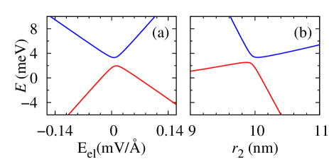
The single particle energy levels obtained within our approach for the fixed distance nm between the dots are shown in Fig. 1(a-b). In Fig. 1a the energy is shown as a function of the external electrical field. Here, both dots have the same size. On the other hand, in Fig. 1b, we show energy dependence on the upper dot size. The size of the lower dot is kept constant, while the base radius of the upper dot and its height are varied, with constant. Electronic (tunnel) coupling between the dots leads to the appearance of an anticrossing pattern. In Fig. 1b it occurs near the point where the dots become equal. In Fig. 1a the resonance is located near the point .
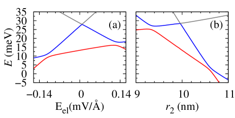
The spectrum of a two-electron system is dominated by antricrossings of different occupation configurations szafran01 ; szafran05 . In Fig. 2 the three lowest spin-singlet eigenstates of the interacting two-electron system are shown. In a similar way as in the one electron case, we present the dependence on the external electrical field (Fig. 2b) and on the upper dot size (Fig. 2a). The central resonance occurs when the doubly occupied configurations have similar energy. This anticrossing is very narrow (less than meV). The other two anticrossings occur at the degeneracy point between the singly occupied configuration and configurations with two electrons in the larger dot. These two splittings are wider than those appearing between the single-electron states, shown in Fig. 1 (2 meV vs. 1.5 meV). It is because the anticrossing of two-electron configurations is enhanced by Coulomb terms grodecka08a .
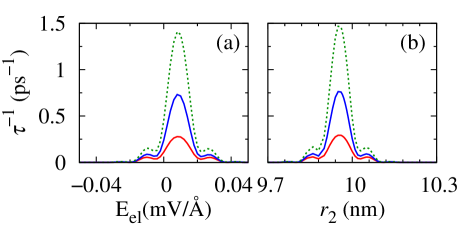
The single particle relaxation rates are shown in Fig. 3 as functions of the upper dot size (Fig. 3b) and the electrical field (Fig. 3a). These results are calculated for the same sample geometries as in Fig. 1 at three different temperatures. The overall magnitude of the relaxation rates depends on the spatial overlap between the wave functions corresponding to the states involved in the transition. This is why the rates are large at the resonance and become smaller when the system is shifted from the resonance point.
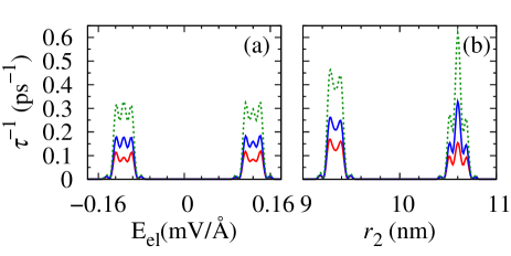
Figs. 4a,b show the relaxation rates for a two electron system. We use the same sample geometries as in the one-electron case and investigate the dependence on electrical field and upper dot size. In general, the relaxation rates are similar to those found in the single electron case. This is due to the fact that both these processes are physically very similar. The only difference is that in the single electron case it tunnels towards an empty QD, whereas in the two electron case, there is already another electron. It leads to shifts (due to Coulomb interaction) to the parameter regimes where energies compensates for the Coulomb repulsion.
IV Conclusion
We have studied the phonon-assisted relaxation (thermalization) for single-electron and two-electron configurations in self-assembled quantum dots. Our model has taken into account the geometry and strain distribution in a QDM. The results show that the phonon relaxation is very efficient in a very narrow range of parameters near the anticrossings of energy levels. We conclude that relaxation times on the order of at least hundreds of picoseconds should be typical. The results for an electric field and various upper dot sizes are quantitatively consistent. Therefore, it is possible to control phonon–induced relaxation by system geometry as well as by an external electric field.
Acknowledgements.
This work was supported by the TEAM programme of the Foundation for Polish Science co-financed from the European Regional Development Fund.References
- (1) R. Heitz, I. Mukhametzhanov, P. Chen, and A. Madhukar, Phys. Rev. B 58, R10151 (1998).
- (2) M. Reischle, G. J. Beirne, R. Roßbach, M. Jetter, H. Schweizer, and P. Michler, Phys. Rev. B 76, 085338 (2007).
- (3) K. Nishibayashi, T. Kawazoe, M. Ohtsu, K. Akahane, and N. Yamamoto, Appl. Phys. Lett. 93, 042101 (2008).
- (4) J. H. Park, D. G. Choi, T. K. Lee, E. Oh, S. Lee, and J. K. Furdyna, Appl. Phys. Lett. 90, 201916 (2007).
- (5) P. Bajracharya, T. A. Nguyen, S. Mackowski, L. M. Smith, H. P. Wagner, U. W. Pohl, D. Bimberg, and M. Strassburg, Phys. Rev. B 75, 035321 (2007).
- (6) F. V. de Sales, S. W. da Silva, J. M. R. Cruz, A. F. G. Monte, M. A. G. Soler, P. C. Morais, M. J. da Silva, and A. A. Quivy, Phys. Rev. B 70, 235318 (2004).
- (7) Y. I. Mazur, Z. M. Wang, G. G. Tarasov, M. Xiao, G. J. Salamo, J. W. Tomm, V. Talalaev, and H. Kissel, Appl. Phys. Lett. 86, 063102 (2005).
- (8) J. Seufert, M. Obert, G. Bacher, A. Forchel, T. Passow, K. Leonardi, and D. Hommel, Phys. Rev. B 64, R121303 (2001).
- (9) A. Tackeuchi, T. Kuroda, K. Mase, Y. Nakata, and N. Yokoyama, Phys. Rev. B 62, 1568 (2000).
- (10) G. Ortner, R. Oulton, H. Kurtze, M. Schwab, D. R. Yakovlev, M. Bayer, S. Fafard, Z. Wasilewski, and P. Hawrylak, Phys. Rev. B 72, 165353 (2005).
- (11) W.-H. Chang, H. Lin, S.-Y. Wang, C.-H. Lin, S.-J. Cheng, M.-C. Lee, W.-Y. Chen, T.-M. Hsu, T.-P. Hsieh, and J.-I. Chyi, Phys. Rev. B 77, 245314 (2008).
- (12) B. D. Gerardot, S. Strauf, M. J. A. de Dood, A. M. Bychkov, A. Badolato, K. Hennessy, E. L. Hu, D. Bouwmeester, and P. M. Petroff, Phys. Rev. Lett. 95, 137403 (2005).
- (13) T. Nakaoka, E. C. Clark, H. J. Krenner, M. Sabathil, M. Bichler, Y. Arakawa, G. Abstreiter, and J. J. Finley, Phys. Rev. B 74, 121305(R) (2006).
- (14) T. Nakaoka, J. Tatebayashi, Y. Arakawa, and T. Saito, J. Appl. Phys. 96, 150 (2004).
- (15) S. Rodt, V. Turck, R. Heitz, F. Guffarth, R. Engelhardt, U. W. Pohl, M. Straßburg, M. Dworzak, A. Hoffmann, and D. Bimberg, Phys. Rev. B 67, 235327 (2003).
- (16) M. Pochwała and P. Machnikowski, Acta Phys. Polon. A 114, 1285 (2008).
- (17) K.Gawarecki, M. Pochwala, A. Grodecka-Grad, and P. Machnikowski, Phys. Rev. B 81, 245312 (2010).
- (18) B. Szafran, S. Bednarek, and J. Adamowski, Phys. Rev. B 64, 125301 (2001).
- (19) B. Szafran, T. Chwiej, F. M. Peeters, S. Bednarek, J. Adamowski, and B. Partoens, Phys. Rev. B 71, 205316 (2005).
- (20) A. Grodecka, P. Machnikowski, and J. Förstner, Phys. Rev. B 78, 085302 (2008).