Optical Probe of Quantum Shot Noise Reduction at a Single-Atom Contact
Abstract
Visible and infra-red light emitted at a Ag-Ag(111) junction has been investigated from tunneling to single atom contact conditions with a scanning tunneling microscope. The light intensity varies in a highly nonlinear fashion with the conductance of the junction and exhibits a minimum at conductances close to the conductance quantum. The data are interpreted in terms of current noise at optical frequencies, which is characteristic of partially open transport channels.
pacs:
72.70.+m,68.37.Ef,73.63.Rt,73.20.MfOwing to the particle nature of the electron, electrical current exhibits noise. The noise spectral density provides information on the conduction process which is complementary to resistance data Blanter and Büttiker (2000). For quantum conductors with a conductance ( is the transmission probability of a conducting quantum state and is the conductance quantum) Landauer (1957, 1988) the spectral density of the noise deviates from Schottky’s classical result Schottky (1918) ( is the average current). is effectively reduced compared to as expressed by the Fano factor Lesovik (1989); Büttiker (1990)
| (1) |
The noise amplitude is particularly large for partially open channels, , where electrons may be either reflected or transmitted, and a drastic reduction occurs when a transport channel is fully open and no reflection takes place. At low frequencies (), this effect has been evidenced for quantum point contacts (QPC) Kumar et al. (1996); Li et al. (1990) and atomic scale metallic contacts van den Brom and van Ruitenbeek (1999). Following a theoretical suggestion of Aguado and Kouwenhoven Aguado and Kouwenhoven (2000), Ghz fluctuations of current in mesoscopic structures have been detected by investigating the transport properties of single Onac et al. (2006); Gustavsson et al. (2008) and double Khrapai et al. (2006); Gustavsson et al. (2007) quantum dots, superconducting mesoscopic photon detectors Deblock et al. (2003), or by using low noise amplifiers followed by detectors Zakka-Bajjani et al. (2007). In these experiments, the quantum detector is located close to the QPC and is sensitive to current shot noise.
Several mechanisms have been proposed to explain how the energy is transferred from the quantum conductor to the quantum detector Khrapai et al. (2006). While a recent experiment by Gustavsson et al. indicates that the process is probably mediated by photons Gustavsson et al. (2008), no direct observation was reported. To enable direct detection of photons, generating current noise in a quantum conductor at frequencies which correspond to visible light would be advantageous. Here, we present the first measurements of shot noise reduction at optical frequencies, which are 3 orders of magnitude higher than previously reported Gustavsson et al. (2008). To this end, we applied elevated voltages up to 2 V to Ag-Ag(111) junctions in a scanning tunneling microscope. Light emitted at the junction was recorded in the far field with detection limits 240 THz 750 THz, which were determined by localized plasmon resonances of the junction and detector response. The conductance of Ag–Ag junctions can be controllably varied close to the contact point enabling significantly more detailed measurements than a previous experiment with Au–Au junctions Schull et al. (2009). The intensity of the emitted light exhibits a clear minimum near , confirming that the light is emitted by current fluctuations. This is the first experimental demonstration of the role of current noise in STM-induced light emission. Moreover, in contrast to expectations Zakka-Bajjani et al. (2007); Aguado and Kouwenhoven (2000); Onac et al. (2006); Gustavsson et al. (2007), shot noise is observed up to frequencies exceeding the limit . This behavior is interpreted in terms of nonlinear electronic processes caused by the intense current passing the atomic size conductor.
The experiments were performed with an ultra high vacuum STM at low temperature (5.8 K). Ag(111) surfaces as well as chemically etched W tips were cleaned by Ar+ bombardment and annealing. To increase the plasmon enhancement the W tips were coated with Ag by indenting them into the sample. As a final step of preparation the tips were repeatedly approached to surface at a sample voltage . This procedure was found to increase the stability of the tips for contact experiments. The unusual currents (typically up to 200 A) and sample voltages (up to 2.0 V) used in the present experiments can lead to significant modifications of both tip and surface. Therefore, topographic images were recorded before and after the acquisition of spectra or the current was monitored during data acquisition to detect abrupt changes, which signal changes of the junction. All data presented here were acquired without changes of the tip or sample. Photons emitted at the tunneling junction were guided with an optical fiber to a grating spectrometer and a liquid nitrogen cooled CCD camera. Spectra are not corrected for the wavelength dependent efficiency of the detection equipment, which has been reported in Ref. Hoffman et al., 2002.
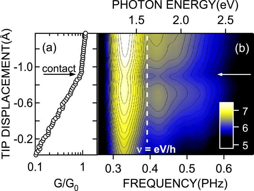
Fig. 1 displays raw data on the light emission from a single atom contact on Ag(111). During a stepwise approach of the STM tip the conductance (Fig. 1(a)) and spectra of the emitted light (Fig. 1(b)) were recorded. The conductance trace exhibits a transition from tunneling to contact (indicated by an arrow) at which is typical of single-atom Ag contacts Agraït et al. (2003); Limot et al. (2005). We note that the smooth evolutions of the conductance and the spectra over the entire range of tip displacements provide additional evidence that no changes of the tip or the sample occurred during the measurement not .
The light emitted from the junction is composed of two components, similar to previous reports from Na monolayers Hoffmann et al. (2003) and Au(111) surfaces Schull et al. (2009). The low-energy emission at photon frequencies is consistent with inelastic one-electron processes. The high-frequency part of the spectra (, cf. dashed vertical line in Fig. 1b) is attributed to processes involving electrons which have been promoted to energies well above the Fermi level via electron-electron scattering. For simplicity, we denote these components and light.
The variations of the and light intensities with the displacement (and, hence, the conductance ) are qualitatively similar. Given the additional complexity of processes we now focus on an analysis of the emission, which is well understood in the tunneling range Johansson et al. (1990); B. N. J. Persson and Baratoff (1992). The intensity as a function of the conductance is displayed in Fig. 2(a). Throughout the tunneling range, at conductances , the intensity increases and is proportional to as expected Johansson et al. (1990). Closer to , however, clear deviations occur, which are more obvious on the linear scales of Fig. 2(b). The intensity decreases despite the continued increase of the current and reaches a minimum at the point of contact formation (Fig. 1(b), arrow). Beyond contact formation, another intensity rise occurs. Similar behavior occurred near integer multiples of the quantum of conductance as illustrated in Fig. 2(b) for not .
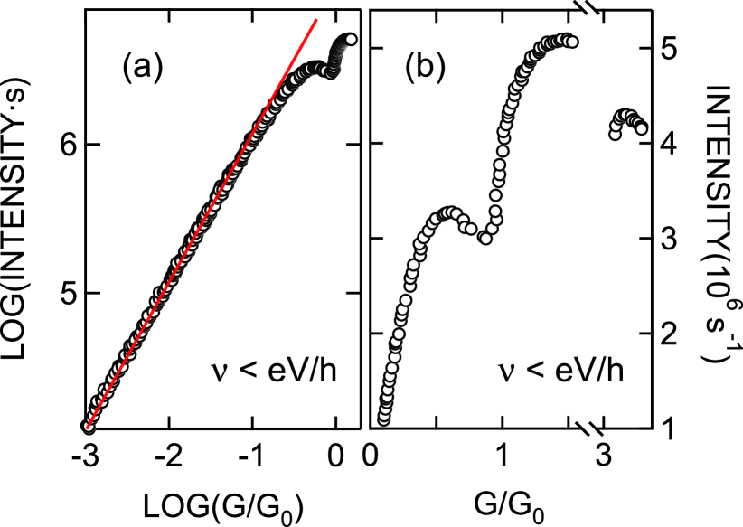
Light emission in the tunneling range, i. e. at low conductance, is mediated by tip-induced plasmon modes (TIP modes), which are induced by the proximity of the STM tip to the sample Johansson et al. (1990); Berndt et al. (1991). These modes, which can decay radiatively, enhance the intensity of the light emitted at TIP resonance frequencies, which, in the case of Ag–Ag junctions, enables light detection in the visible and near infra-red range. Except for a small red-shift () of the peak aiz02 with tip approach, no major change of the spectral shape was observed, implying that the TIP modes remain largely unchanged over the tip excursion of probed in Fig. 1. The drastic 70% decrease of the photon yield (Fig. 3) can hardly be explained by this red-shift. However, the plasmon modes are driven by fluctuations of the tunneling current Rendell1978 ; Laks1979 ; Johansson et al. (1990). For this reason, the light intensity may be expected to be proportional to the high-frequency shot noise of the tunneling current. We propose the hypothesis that this linear relation remains valid close to and at contact. The reduced light intensity near would then reflect the different noise characteristics at large conductances. Indeed, model calculations as well as experiments have shown that the low-frequency shot noise of a quantum contact is reduced below its classical value as described by the Fano factor of Eq. 1 Lesovik (1989); Büttiker (1990); Kumar et al. (1996); Li et al. (1990); van den Brom and van Ruitenbeek (1999).
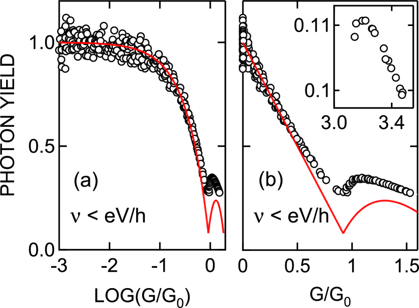
To test our hypothesis, Fig. 3 shows a comparison of the yield of light (circles), which we define as the intensity per current, and the Fano factor (line). The yield is normalized to 1 at low conductance values. As a minimal model of the Fano factor, we used two conductance channels, similar to the approach of van den Brom and van Ruitenbeek van den Brom and van Ruitenbeek (1999) (specifically, for , we set and and, for , and ). Fig. 3(a) covers more than three decades of conductance on a logarithmic scale. The experimental results in the tunneling range, which corresponds to the limit of an almost closed conductance channel, are consistent with the previous data reported by various researchers from various samples, where a linear relationship between intensity and current was observed. Clear deviations from this linearity become obvious for , where a drastic reduction of the yield is observed. The experimental data is described rather accurately by the Fano factor model.
The yield at conductances close to is shown in more detail in Fig. 3(b) on a linear scale. It assumes a minimum at , i. e. the conductance typically observed from a single atom Ag contact (cf. Fig. 1(a)). At higher conductances, upon further approach of the STM tip, the yield recovers, and goes through a maximum followed by another reduction. These variations are qualitatively reproduced by the Fano factor within the two-channel model. Similarly, the variation of the yield between 3 and 4 (Fig. 3(b) inset) is consistent with the Fano factor describing a 3 atom contactvan den Brom and van Ruitenbeek (1999). This lends strong support to the hypothesis that the light intensity is directly related to the current noise.
The role of shot noise of quantum conductors as a source for the electromagnetic radiation has been theoretically discussed Lesovik and Loosen (1997); Gavish et al. (2000); Aguado and Kouwenhoven (2000); Beenakker and Schomerus (2001, 2004) and indirect experimental evidence of the emission of light was found from the transport properties of various quantum detectors located in the near field of a noise source Onac et al. (2006); Gustavsson et al. (2008); Khrapai et al. (2006); Gustavsson et al. (2007); Deblock et al. (2003); Zakka-Bajjani et al. (2007). The present experiment is the first one to directly demonstrate that the current shot noise of a quantum point contact leads to the emission of sub-PHz radiation into the far field.
Despite the similarities of the model and the data, there are deviations. Most notably, the intensity reduction at is less complete than expected from the model. This may partially be due to the presence of more than two open channels. While previous results from Ag break junctions indicate that the contribution of additional channels is minor Ludoph and van Ruitenbeek (2000), the significantly higher bias voltages used in the present experiments are expected to modify the related transmission probabilities. Heating of the electron gas is another likely explanation of the incomplete noise reduction. Thermal fluctuations at a temperature lead to the following noise spectral density Büttiker (1992)
Using this expression, the limited intensity reduction in the experiment can be fitted not assuming an electron temperature .
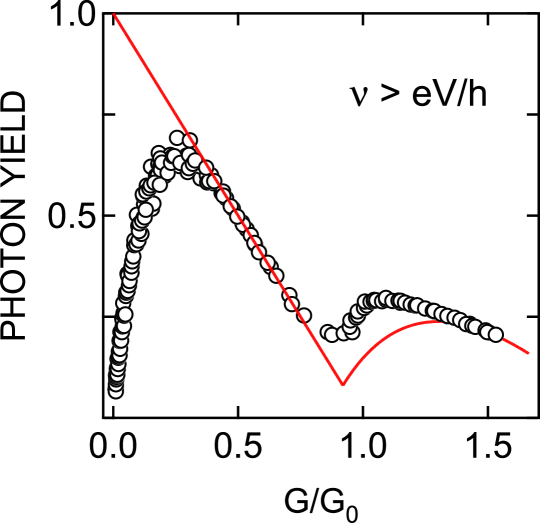
The yield of light varies in an intriguing manner (Fig. 4). While it is zero in the limit of vanishing conductance, an increase is observed up to . At higher conductances, the experimental data approaches the behavior observed for light, i. e., it is rather close to the Fano factor (solid line). As previously demonstrated light may be attributed to inelastic transitions involving electrons which have been promoted to energies above the Fermi edge through electron-electron scattering Hoffmann et al. (2003); Schull et al. (2009). We propose that the number of these electrons is low at low and effectively limits the yield. At sufficiently high , however, the yield tends to reflect current noise at frequencies as described by the Fano factor.
In summary, the intensity of light emitted from single atom silver contacts exhibits a highly nonlinear variation with the conductance. The intensity variation is interpreted in terms of a progressive reduction of high frequency shot noise. An unexpected noise component at is observed and interpreted in terms of non-linear electronic processes. Finally, the results reveal a link between plasmon-mediated inelastic tunneling and current noise and raise intriguing questions into the interaction of electrons in single atom contacts with local optical modes.
We thank F. Charra, T. Frederiksen and P. Johansson, for discussions. Financial support by the Innovationsfonds Schleswig-Holstein is gratefully acknowledged.
References
- (1)
- (2)
- Blanter and Büttiker (2000) Y. M. Blanter and M. Büttiker, Phys. Rep. 336, 1 (2000).
- Landauer (1957) R. Landauer, IBM J. Res. Dev. 1, 223 (1957).
- Landauer (1988) R. Landauer, IBM J. Res. Dev. 32, 306 (1988).
- Schottky (1918) W. Schottky, Ann. Phys. (Leipzig) 362, 541 (1918).
- Lesovik (1989) G. B. Lesovik, Pis’ma Zh. Eksp. Teor. Fiz. 49, 513 (1989), [Sov. Phys. JETP Lett. 49, 592 (1989)].
- Büttiker (1990) M. Büttiker, Phys. Rev. Lett. 65, 2901 (1990).
- Kumar et al. (1996) A. Kumar, L. Saminadayar, D. C. Glattli, Y. Jin, and B. Etienne, Phys. Rev. Lett. 76, 2778 (1996).
- Li et al. (1990) Y. P. Li, D. C. Tsui, J. J. Heremans, J. A. Simmons, and G. W. Weimann, Appl. Phys. Lett. 57, 774 (1990).
- van den Brom and van Ruitenbeek (1999) H. E. van den Brom and J. M. van Ruitenbeek, Phys. Rev. Lett. 82, 1526 (1999).
- Aguado and Kouwenhoven (2000) R. Aguado and L. P. Kouwenhoven, Phys. Rev. Lett. 84, 1986 (2000).
- Onac et al. (2006) E. Onac, F. Balestro, L. H. Willems van Beveren, U. Hartmann, Y. V. Nazarov, and L. P. Kouwenhoven, Phys. Rev. Lett. 96, 176601 (2006).
- Gustavsson et al. (2008) S. Gustavsson, I. Shorubalko, R. Leturcq, T. Ihn, K. Ensslin, and S. Schön, Phys. Rev. B 78, 035324 (2008).
- Khrapai et al. (2006) V. S. Khrapai, S. Ludwig, J. P. Kotthaus, H. P. Tranitz, and W. Wegscheider, Phys. Rev. Lett. 97, 176803 (2006).
- Gustavsson et al. (2007) S. Gustavsson, M. Studer, R. Leturcq, T. Ihn, K. Ensslin, D. C. Driscoll, and A. C. Gossard, Phys. Rev. Lett. 99, 206804 (2007).
- Deblock et al. (2003) R. Deblock, E. Onac, L. Gurevich, and L. P. Kouwenhoven, Science 301, 203 (2003).
- Zakka-Bajjani et al. (2007) E. Zakka-Bajjani, J. Ségala, F. Portier, P. Roche, D. C. Glattli, A. Cavanna, and Y. Jin, Phys. Rev. Lett. 99, 236803 (2007).
- Schull et al. (2009) G. Schull, N. Neel, P. Johansson, and R. Berndt, Phys. Rev. Lett. 102, 057401 (2009).
- Hoffman et al. (2002) G. Hoffman, J. Kröger, and R. Berndt, Rev. Sci. Instrum. 73, 305 (2002).
- Agraït et al. (2003) N. Agraït, A. L. Yeyati, and J. M. van Ruitenbeek, Phys. Rep. 377, 81 (2003).
- Limot et al. (2005) L. Limot, J. Kröger, R. Berndt, A. Garcia-Lekue, and W. A. Hofer, Phys. Rev. Lett. 94, 126102 (2005).
- (23) When contacting a clean Ag(111) terrace no transfer of an atom from the tip to the surface was observed at the voltages used here, in contrast to the case of low bias voltages Limot et al. (2005). Spectroscopic results and conductance data were very similar for contacts to flat areas and adatoms.
- Hoffmann et al. (2003) G. Hoffmann, R. Berndt, and P. Johansson, Phys. Rev. Lett. 90, 046803 (2003).
- Johansson et al. (1990) P. Johansson, R. Monreal, and P. Apell, Phys. Rev. B 42, 9210 (1990).
- B. N. J. Persson and Baratoff (1992) B. N. J. Persson and A. Baratoff, Phys. Rev. Lett. 68, 3224 (1992).
- (27) The complex pattern of decreasing and increasing intensity is clear indication that effects such as shadowing of the emission, changes of the emission direction close to contact or a voltage drop in the contact region can be excluded as possible origins of the intensity variations.
- Berndt et al. (1991) R. Berndt, J. K. Gimzewski, and P. Johansson, Phys. Rev. Lett. 67, 3796 (1991).
- (29) J. Aizpurua, G. Hoffmann, S. P. Apell, and R. Berndt, Phys. Rev. Lett. 89, 156803 (2002).
- (30) R.W. Rendell, D.J. Scalapino, and B. Mühlschlegel, Phys. Rev. Lett. 41, 1746 (1978).
- (31) B. Laks, and D.L. Mills, Phys. Rev. B 20, 4962 (1979).
- Lesovik and Loosen (1997) G. B. Lesovik and R. Loosen, Pis’ma Zh. Eksp. Teor. Fiz. 65, 280 (1997), [Sov. Phys. JETP Lett. 65, 295 (1997)].
- Gavish et al. (2000) U. Gavish, Y. Levinson, and Y. Imry, Phys. Rev. B 62, R10637 (2000).
- Beenakker and Schomerus (2001) C. W. J. Beenakker and H. Schomerus, Phys. Rev. Lett. 86, 700 (2001).
- Beenakker and Schomerus (2004) C. W. J. Beenakker and H. Schomerus, Phys. Rev. Lett. 93, 096801 (2004).
- Ludoph and van Ruitenbeek (2000) B. Ludoph and J. M. van Ruitenbeek, Phys. Rev. B 61, 2273 (2000).
- Büttiker (1992) M. Büttiker, Phys. Rev. B 46, 12485 (1992).
- (38) The range of minimum photon yield, where the Fano factor is minimal at , was used for the fit.
- (39) For an order-of-magnitude estimate of the absolute quantum efficiencies we considered the detected solid angle and assumed an isotropic emission. The wavelength dependent efficiency of the detection setup was taken into account.