Precise in-situ tuning of a superconducting nanowire’s critical current using high bias voltage pulses
Abstract
We present a method for in-situ tuning the critical current (or switching current) and critical temperature of a superconducting nanowire using high bias voltage pulses. Our main finding is that as the pulse voltage is increased, the nanowires demonstrate a reduction, a minimum and then an enhancement of the switching current and critical temperature. Using controlled pulsing, the switching current of a superconducting nanowire can be set exactly to a desired value. These results correlate with in-situ transmission electron microscope imaging where an initially amorphous nanowire transforms into a single crystal nanowire by high bias voltage pulses.
Superconducting nanowires have been proposed as candidates for various solid state qubit implementations Mooij and Harmans (2005); Mooij and Nazaron (2006); Ku et al. (2010). We describe a post-fabrication technique using high bias voltage pulses that allows in-situ precise control over the critical current which may be highly instrumental in developing superconducting nanowire qubits.
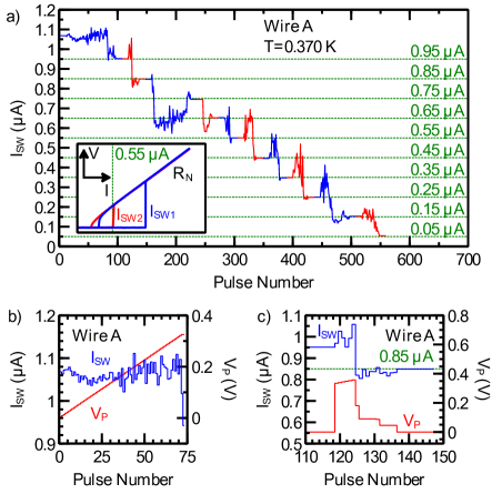
As high bias pulses are applied to superconducting MoGe nanowires, we observe a decrease of switching current, , which is measured at a fixed temperature, typically 0.3K. Analysis of the rate of Little’s phase slips indicates that pulsing also causes a decrease in the critical temperature, , of the wire. An interesting application of this effect is to precisely control the switching current of a superconducting nanowire in-situ. We demonstrate that the switching current can be set to within approximately 10 nA of a desired value (see figure 1a). The switching current cannot be more accurately defined as it is natural stochastic due to thermal and quantum fluctuations Sahu et al. (2009).
The nanowires were fabricated using the method of molecular templating Bezryadin et al. (2000). Both single-walled (SWNT) and multi-walled (MWNT) carbon nanotubes suspended across a trench were coated with Mo76Ge24 to form the nanowires (no difference was observed in behavior between SWNT and MWNT). Single voltage pulses were applied by using relays to switch from a quasi-four probe measurement to a single voltage pulse source. No effect on any nanowire was observed from just switching the relays without pulse application. The pulse length was kept fixed at 100 s and was checked to transmit through the filtering of the cryostat to the sample.
From voltage vs current measurements, we can extract the switching current, , and the normal resistance, , (see inset of figure 1a) versus pulse number or pulse voltage, , applied to the nanowire. The effect as is increased from to V in mV steps is shown in figure 1b. As is increased, we observe an increasing stochasticity of which quickly becomes greater than the natural stochasticity of the switching current. As increases further, we see a sharp, downward trend of . It should be noted that was always measured sufficiently after the voltage pulse was finished that the wire had time to completely equilibrate to the bath temperature. Thus the observed changes in are due to the voltage pulse permanently altering the wire and not heating effects of the high bias pulse. We can use this combined downward trend and increased stochasticity to precisely set to a desired value. In figure 1a, is set to ten values chosen uniformly from A to A. An example of a pulse sequence used to set is shown in figure 1c. Large pulses are used to approach the desired value and then smaller pulses are used to ‘bounce’ the switching current to within nA of the desired value. For each of the ten chosen target values, the switching current was set to the desired value.
As is increased further, saturates at a minimum and then counterintuitively begins to increase, returning to values similar to or even exceeding the starting value of . The drop, saturation and recovery of can be see in figure 2a and 2b. The initial drop of does not have a corresponding change in . When reaches a minimum and then begins to increase, begins to drop. This behavior was reproduced on many nanowires of which figure 2 contains two examples. SEM imaging of wires before and after pulsing do not indicate any formation of weak links due to pulsing.
Weak links would only account for the reduction of switching current and not explain the observed recovery of with increased pulse voltage. In-situ TEM imaging of a nanowire during pulsing indicates the initially amorphous nanowire becomes crystallized as pulsing proceeds. In figure 2c, an unpulsed, amorphous Mo76Ge24 wire is shown with the crystal structure of the underlying MWNT (measured line spacing Å) visible in the bottom half of the image. The crystallization begins by forming polycrystals in the center of the nanowire and gradually annealing the nanowire into a single crystal (measured line spacing Å) as shown in figure 2d.
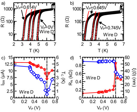
The resistance versus temperature curves taken after a series of pulsing are shown in figure 3a and 3b. The critical temperature, , of the nanowire decreases as pulse voltage increases saturating at a minimum. is defined as a fitting parameter in the best Little fit (discussed in detail below). Further increase of pulse voltage results in the increase of and a drop in (see figure 3c and 3d).
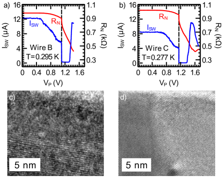
Most forms of crystalline MoGe have lower ’s than amorphous MoGe Ghosh and Douglass (1977) so it is not surprising that the crystallization of MoGe would reduce the wire’s critical temperature thereby reducing critical current at a given temperature. It can be expected that any crystallization or segregation of the MoGe alloy from the large current pulse would produce a reduction of .
The observed crystallization of the MoGe is caused by a combination of electromigrationPark et al. (1999); Strachan et al. (2008); Heersche et al. (2007) and Joule heating induced thermal effects. It appears that thermal effects are dominant since we observe the appearance of crystals at the center hottest spot of the wire and also do not observe the weak link formation associated with electromigration. As a rough approximation of the temperature of the nanowire, we can write the applied voltage as a function of temperature (assuming a constant resistivity): where is the voltage of the pulse, is the Lorenz number, is the temperature of the wire center and is the temperature of the electrodes Holm (1967). Typical values (V=0.5V) gives us an estimated temperature of K close to the crystalizing temperature of MoGe.
The particular crystal form of MoGe closest to our starting concentration of Mo76Ge24 is Mo3Ge which is an A15 compound (known to have high ’s). Studies on Mo3Ge reveal that its is highly dependent on formation conditions (i.e. it can have a very low ) but under the correct formation conditions, the can exceed 5.7K (comparable to the critical temperature of the starting amorphous MoGe) Ghosh and Douglass (1977). It has been observed experimentally that Mo3Ge can be generated by heating amorphous MoGe to high temperatures Searcy et al. (1952). Thus we propose that the return and sometimes higher is caused by the formation of relatively well-ordered crystal Mo3Ge from Joule heating by the high bias pulses. Comparison of TEM images measured line spacing (see figure 2c and d) to x-ray diffraction data Searcy et al. (1952) conclusively indicate that the crystal formed is indeed Mo3Ge. To compare to previous experiments on nanowires we use a phenomenological Little thermally activated phase slip (TAPS) model Bezryadin (2008): where is the normal resistance of the nanowire, is the free energy barrier for phase slips, is the Boltzmann constant and is temperature Chu et al. (2004); Tinkham (1996); Langer and Ambegaokar (1967); Bezryadin (2008). The temperature dependence of the free energy barrier is accurately given at all temperatures by the Bardeen formula Bardeen (1962): where we can express using experimentally accessible parameters Tinkham and Lau (2002). This model is used to produce the fits shown in figure 3 where the fitting parameters are critical temperature, , and coherence length, .
As shown in figure 3c, the decrease and return of corresponds to a drop and return of as expected. In figure 3d, we see that is stable and coherence length is gradually increasing as would be expected from the corresponding decrease in Tinkham (1996). When saturates at a minimum and begins to increase, starts to decrease. Likewise, the coherence length returns from a maximal value (the maximum being due to a highly reduced ) and approaches a value higher than its initial value. This is reasonable since as the wire becomes well-ordered crystalline Mo3Ge, we anticipate an enhanced coherence length due to the longer mean free path of the crystal compared to amorphous MoGe. From a simple Drude model of resistivity, a longer mean free path also implies a decreased normal resistance in agreement with the observed drop in resistance.
In conclusion, we demonstrate that controlled high bias pulsing can be used to precisely set the switching current of the nanowire and that the counterintuitive decrease and increase of the switching current with increasing pulse voltage is well explained by crystallization induced by Joule heating.
Acknowledgements.
We thank Jian-Guo Wen for help with the TEM analysis. This material is based upon work supported by NSF-DMR 10-05645 and by the U.S. Department of Energy under grants DE-FG02-07ER46453 and DE-FG02-07ER46471 through the Frederick Seitz Materials Research Laboratory at the University of Illinois at Urbana-Champaign.References
- Mooij and Harmans (2005) J. E. Mooij and C. J. P. M. Harmans, New Journal of Physics, 7, 219 (2005).
- Mooij and Nazaron (2006) J. E. Mooij and Y. V. Nazaron, Nature Physics, 2, 169 (2006).
- Ku et al. (2010) J. Ku, V. Manachurian, and A. Bezryadin, “Superconducting Nanowires as Nonlinear Inductive Elements for Qubits,” Physical Review B, 82, 134518 (2010).
- Sahu et al. (2009) M. Sahu, M. Bae, A. Rogachev, D. Pekker, T. Wei, N. Shah, P. Goldbart, and A. Bezryadin, “Individual topological tunnelling events of a quantum field probed through their macroscopic consequences,” Nature Physics, 5, 503 (2009).
- Bezryadin et al. (2000) A. Bezryadin, C. N. Lau, and M. Tinkham, “Quantum suppression of superconductivity in ultrathin nanowires,” Nature, 404, 971 (2000).
- Ghosh and Douglass (1977) A. K. Ghosh and D. H. Douglass, Journal of Low Temperature Physics, 27, 487 (1977).
- Park et al. (1999) H. Park, A. Lim, A. Alivisatos, J. Park, and P. McEuen, “Fabrication of metallic electrodes with nanometer separation by electromigration,” Applied Physics Letters, 75, 301 (1999).
- Strachan et al. (2008) D. R. Strachan, D. E. Johnston, B. S. Guiton, S. S. Datta, P. K. Davies, D. A. Bonnell, and A. T. C. Johnson, “Real-time tem imaging of the formation of crystalline nanoscale gaps,” Physical Review Letters, 100, 056805 (2008).
- Heersche et al. (2007) H. B. Heersche, G. Lientschnig, K. O Neill, H. van der Zant, and H. Zandbergen, “In situ imaging of electromigration-induced nanogap formation by transmission electron microscopy,” Applied Physics Letters, 91, 072107 (2007).
- Holm (1967) R. Holm, Electrical Contacts (Springer-Verlag, 1967).
- Searcy et al. (1952) A. W. Searcy, R. J. Peavler, and H. J. Yearian, “Preparation of mo3ge and determination of its structure,” Journal of the American Chemical Society, 74, 566 (1952).
- Bezryadin (2008) A. Bezryadin, Journal of Physics: Condensed Matter, 20, 043202 (2008).
- Chu et al. (2004) S. L. Chu, A. T. Bollinger, and A. Bezryadin, “Phase slips in superconducting films with constrictions,” Physical Review B (Condensed Matter and Materials Physics), 70, 214506 (2004).
- Tinkham (1996) M. Tinkham, Introduction to Superconductivity (Dover Publications, 1996).
- Langer and Ambegaokar (1967) J. S. Langer and V. Ambegaokar, “Intrinsic resistive transition in narrow superconducting channels,” Physical Review, 164, 498 (1967).
- Bardeen (1962) J. Bardeen, “Critical fields and currents in superconductors,” Reviews of Modern Physics, 34, 667 (1962).
- Tinkham and Lau (2002) M. Tinkham and C. N. Lau, “Quantum limit to phase coherence in thin superconducting wires,” Applied Physics Letters, 80, 2946 (2002).