STM and RHEED study of the Si(001)-c surface
Abstract
The Si(001) surface deoxidized by short annealing at C in the ultrahigh vacuum molecular beam epitaxy chamber has been in situ investigated by high resolution scanning tunnelling microscopy (STM) and reflected high energy electron diffraction (RHEED). RHEED patterns corresponding to and structures were observed during sample treatment. The reconstruction arose at C after annealing. The reconstruction was observed to be reversible: the structure turned into the one at C, the structure appeared again at recurring cooling. The reconstruction was revealed by STM at room temperature on the same samples. A fraction of the surface area covered by the structure decreased as the sample cooling rate was reduced. The structure was observed on the surface free of the one. The structure has been evidenced to manifest itself as the one in the RHEED patterns. A model of the structure formation has been built on the basis of the STM data. Origin of the high-order structure on the Si(001) surface and its connection with the epinucleation phenomenon are discussed.
keywords:
Silicon , Surface reconstruction , Scanning tunnelling microscopy , Reflected high energy electron diffractionPACS:
68.35.B- , 68.37.Ef , 68.49.Jk , 68.47.Fg, , url]www.gpi.ru/eng/staff_s.php?eng=1&id=125
1 Introduction
Investigations of clean silicon surfaces prepared in conditions of actual technological chambers are of great interest due to the industrial requirements to operate on nanometer and subnanometer scale when designing future nanoelectronic devices [1]. In the nearest future, the sizes of structural elements of such devices will be close to the dimensions of structure features of Si(001) surface, at least of its high-order reconstructions such as . Most of researches of the Si(001) surface have thus far been carried out in specially refined conditions which allowed one to study the most common types of the surface reconstructions such as , , or [2, 3, 4, 5, 6, 7, 8, 9, 10, 11, 12, 13, 14]. Unfortunately, no or very few papers have thus far been devoted to investigations of the Si surface which is formed as a result of the wafer cleaning and deoxidation directly in the device manufacturing equipment [14]. But anyone who deals with Si-based nanostructure engineering and the development of such nanostructure formation cycles compatible with some standard device manufacturing processes meets the challenging problem of obtaining the clean Si surface within the imposed technological restrictions which is one of the key elements of the entire structure formation cycle [1, 15, 16].
The case is that the ambient in technological vessels such as molecular beam epitaxy (MBE) chambers is usually not as pure as in specially refined ones designed for surface studies. There are many sources of surface contaminants in the process chambers including materials of wafer heaters or evaporators of elements as well as foreign substances used for epitaxy and doping. In addition, due to technological reasons the temperature treatments applicable for device fabrication following the standard processes such as CMOS often cannot be as aggressive as those used for surface preparation in the basic experiments. Moreover, the commercially available technological equipment sometimes does not enable the wishful annealing of Si wafers at the temperature of C even if the early device formation stage allows one to heat the wafer to such a high temperature. Nevertheless, the technologist should always be convinced that the entirely deoxidized and atomically clean Si surface is reliably and reproducibly obtained.
A detailed knowledge of the Si surface structure which is formed in the above conditions—its reconstruction, defectiveness, fine structural peculiarities, etc.—is of great importance too because this structure may affect the properties of nanostructured layers deposited on it. For instance, the Si surface structure may affect the magnitude and the distribution of the surface stress of the Ge wetting layer on nanometer scale when the Ge/Si structure is grown, which in turn affect the Ge nanocluster nucleation and eventually the properties of quantum dot arrays formed on the surface [1, 16, 17, 18, 19, 20, 21, 22, 23, 24, 25, 26, 27, 28, 29, 30].
Thus, it is evident from the above that the controllable formation of the clean Si(001) surface with the prescribed parameters required for technological cycles of nanofabrication compatible with the standard device manufacturing processes should be considered as an important goal, and this article presents a step to it.
In the present paper, we report the results of investigation of the Si(001) surface treated following the standard procedure of Si wafer preparation for the MBE growth of the SiGe/Si(001) or Ge/Si(001) heterostructures. A structure arising on the Si(001) surface as a result of short high-temperature annealing for SiO2 removal is explored. It is well known that such experimental treatments favor the formation of nonequilibrium structures on the surface. The most studied of them are presently the and ones. This work experimentally investigates by means of scanning tunneling microscopy (STM) and reflected high energy electron diffraction (RHEED) the formation and atomic structure of the less studied high-order (or [14, 15, 16]) reconstruction. Observations of this reconstruction have already been reported in the literature [4, 5, 6, 10] but there is no clear comprehension of causes of its formation as the structures looking like the one appear after different treatments: The reconstruction was observed to be a result of the coper atoms deposition on the Si(001)- surface [7, 10]; similar structures were found to arise due to various treatments and low-temperature annealing of the original Si(001)- surface without deposition of any foreign atoms [4, 5, 6]. Data of the STM studies of the Si(001)- surface were presented in Refs. [5, 10].
It may be supposed on the analogy with the Si(001)- reconstruction [12, 31, 32, 33, 34, 35] that the presence of impurity atoms on the surface as well as in the subsurface regions is not the only reason of formation of reconstructions different from the one, and the conditions of thermal treatments should be taken into account. The results of exploration of effect of such factor as the rate of sample cooling from the annealing temperature to the room one on the process of the reconstruction formation are reported in the present article. It is shown by means of RHEED that the diffraction patterns corresponding to the surface structure reversibly turn into those corresponding to the one depending on the sample temperature, and a point of this phase transition is determined. Based on the STM data a model of the structure formation is brought forward.
2 Methods and equipment
The experiments were made using an integrated ultra-high-vacuum (UHV) system [27] based on the Riber EVA 32 molecular beam epitaxy chamber equipped with the Staib Instruments RH20 diffractometer of reflected high energy electrons and coupled through a transfer line with the GPI 300 UHV scanning tunnelling microscope [36, 37, 38]. This instrument enables the STM study of samples at any stage of Si surface preparation and MBE growth. The samples can be serially moved into the STM chamber for the analysis and back into the MBE vessel for further treatments as many times as required never leaving the UHV ambient. RHEED experiments can be carried out in situ, i.e. directly in the MBE chamber during the process.
Samples for STM were 88 mm2 squares cut from the specially treated commercial B-doped CZ Si wafers (-type, cm). RHEED measurements were carried out at the STM samples and similar wafers; the samples were investigated only by means of RHEED. After chemical treatment following the standard procedure described elsewhere [1, 39] (which included washing in ethanol, etching in the mixture of HNO3 and HF and rinsing in the deionized water), the samples were placed in the holders. The STM samples were mounted on the molybdenum STM holders and inflexibly clamped with the tantalum fasteners. The STM holders were placed in the holders for MBE made of molybdenum with tantalum inserts. The wafers were inserted directly into the standard molybdenum MBE holders and did not have so hard fastening as the STM samples.
Thereupon the samples were loaded into the airlock and transferred into the preliminary annealing chamber where outgassed at C and Torr for about 6 hours. After that the samples were moved for final treatment and decomposition of the oxide film into the MBE chamber evacuated down to Torr. There were two stages of annealing in the process of sample heating —at C for min and at C for min [1, 14, 27]. The final annealing at C took min with maximum temperature C (C for min) [27]. Then the temperature was rapidly lowered to C. The rates of the further cooling down to the room temperature were C/s (referred to as the “quenching” mode of both the STM samples and wafers) or C/s (called the “slow cooling” mode of only the STM samples) (Fig. 1). The pressure in the MBE chamber increased to Torr during the process.

In both chambers, the samples were heated from the rear side by radiators of tantalum. The temperature was monitored with the IMPAC IS 12-Si pyrometer which measured the Si sample temperature through chamber windows. The atmosphere composition in the MBE camber was monitored using the SRS RGA-200 residual gas analyser before and during the process.
After cooling, the STM samples were moved into the STM chamber in which the pressure did not exceed Torr. REED patterns were obtained for all samples directly in the MBE chamber at different elevated temperatures in the process of the sample treatment and at room temperature after cooling. The STM samples were always explored by RHEED before moving into the STM chamber.
The STM tips were ex situ made of the tungsten wire and cleaned by ion bombardment [40] in a special UHV chamber connected to the STM chamber. The STM images were obtained in the constant tunnelling current mode at room temperature. The STM tip was zero-biased while the sample was positively or negatively biased when scanned in empty or filled states imaging mode.
The STM images were processed afterwords using the WSxM software [41].
3 Experimental findings
(a)
 (b)
(b)

(a)
 (b)
(b)
 (c)
(c)
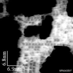
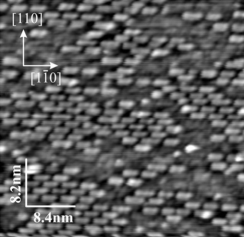
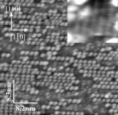
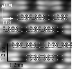
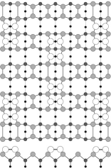
Fig. 2 demonstrates STM images of the Si(001) surface after annealing at C of different duration. Fig. 2a depicts the early phase of the oxide film removal; the annealing duration is 2 min. A part of the surface is still oxidized: the dark areas in the image correspond to the surface coated with the oxide film. The lighter areas correspond to the purified surface. A structure of ordered “rectangles” (the grey features) is observed on the deoxidizes surface. After longer annealing (for 3 min.) and quenching (Fig. 1), the surface is entirely purified of the oxide (Fig. 2b). It consists of terraces separated by the or monoatomic steps with the height of Å [3]. Each terrace is composed of rows running along or directions. The surface reconstruction is different from the one. The insert of Fig. 2b demonstrates the Fourier transform of this image which corresponds to the structure [5]: Reflexes of the Fourier transform correspond to the distance Å in both and directions. So the revealed structure have a periodicity of Å that corresponds to 8 translations on the surface lattice of Si(001) along the 110 directions ( Å is a unit translation length). Rows consisting of structurally arranged rectangular blocks are clearly seen in the empty state STM image (Fig. 2b). They turn by on the neighbouring terraces.
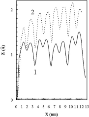
Fig. 3 demonstrates the empty and filled state images of the same surface region. Each block consists of two lines separated by a gap. This fine structure of blocks is clearly seen in the both pictures (a) and (b) but its images are different in different scanning modes. A characteristic property most clearly seen in the filled state mode (Fig. 3b) is the presence of the brightness maxima on both sides of the lines inside the blocks. These peculiar features are described below in more detail. Fig. 3c shows the profiles of the images taken along the white lines. Extreme positions of both curves are well fitted. Relative heights of the features outside and inside the blocks can be estimated from the profiles.

(a)
 (b)
(b)
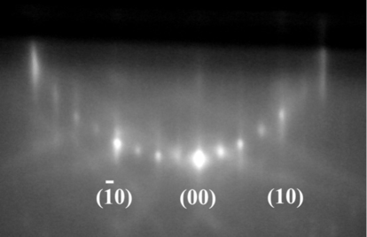
Fig. 4 demonstrates typical RHEED patterns taken at room temperature from the STM sample annealed for 3 min. with further quenching. Characteristic distances on the surface corresponding to the reflex positions in the diffraction pattern were calculated according to Ref. [42]. The derived surface structure is . One sample showed the RHEED patterns corresponding to the structure [42] after the same treatment though.
Temperature dependences of the RHEED patterns in the 110 azimuth were investigated during sample heating and cooling. It was found that the reflexes corresponding to were distinctly seen in the RHEED patterns during annealing at C after 2 minutes of treatment. The reflexes corresponding to started to appear during sample quenching and became definitely visible at the temperature of C; a weak signal started to arise at C if the sample was cooled slowly (Fig. 1). At the repeated heating from room temperature to C, the structure disappeared at C giving place to the one. The structure appeared again at during recurring cooling.
The RHEED patterns obtained from samples always corresponded to the reconstruction. Diffraction patterns for the STM sample which was not hard fastened to the holder corresponded to the structure after quenching (STM measurements were not made for this sample).
(a)
 (b)
(b)
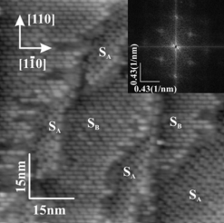
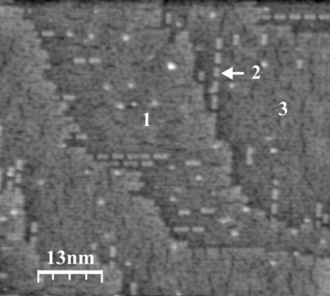
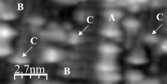
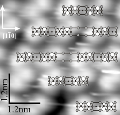
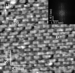
Effects of annealing duration and cooling rate on the clean surface structure were studied by STM. It was established that increase of annealing duration to 6 min. did not cause any changes of the surface structure. On the contrary, decrease of the sample cooling rate drastically changes the structure of the surface. The STM images of the sample surface for the slow cooling mode (Fig. 1) are presented in Fig. 5. The difference of this surface from that of the quenched samples (Fig. 2b) is that only a few rows of “rectangles” are observed on it. The order of the “rectangle” positions with the period of remains in such rows. Two adjacent terraces are designated in Fig. 5a by figures ‘1’ and ‘3’. A row of “rectangles” marked as ‘2’ is situated on the terrace ‘3’; it has the same height as the terrace ‘1’. The filled state image, which is magnified in comparison with the former one, is given in Fig. 5b. A part of the surface free of the “rectangles” is occupied by the reconstruction. Images of the dimer rows with the resolved Si atoms are marked as ‘B’ in Fig. 5b. The “rectangles” are also seen in the image (they are marked as ‘A’) as well as single defects: dimerized Si atoms (‘C’) and chaotically located on the surface accumulations of several dimers. Most of these dimers are oriented parallel to dimers of the lower surface and located strictly on the dimer row. Note that influence of the cooling rate on the surface structure was observed by the authors of Ref. [6]: when the sample cooling rate was decreased the surface reconstruction turned from to which was considered as the derivative reconstruction of the one transformed because of dimer buckling.
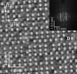
Fig. 6 presents the STM images obtained for the samples cooled in the quenching mode but containing ares free of “rectangles”. The images (a) and (b) of the same place on the surface were obtained serially one by one. We managed to image the surface structure between the areas occupied by the “rectangle” rows, but only in the filled state mode (see the insert at Fig. 6b). Like in Fig. 5b this structure is seen to be formed by parallel dimer rows going apart. The direction of these rows is perpendicular to the direction of the rows of “rectangles”. The height difference of the rows of “rectangles” and the rows is 1 monoatomic step ( Å). We did not succeed to obtain a good enough image of these subjacent dimer rows in the empty state mode. It should be noted also that positions of the “rectangles” are always strictly fixed relative to the dimer rows of the lower layer: they occupy exactly three subjacent dimer rows. It also may be seen in the STM images presented in Refs. [5, 10].
(a)
 (b)
(b)
3.1 Fine structure of the observed reconstruction
Let us consider the observed structure in detail.
A purified sample surface consists of monoatomic steps. Following the nomenclature by Chadi [3], they are designated as and in Fig. 2b. Each terrace is composed by rows running along the or directions. Each row consists of rectangular blocks (“rectangles”). They may be regarded as surface structural units as they are present on the surface after thermal treatment in any mode, irrespective of a degree of surface coverage by them. Reflexes of the Fourier transform of the picture shown in Fig. 2b correspond to the distances and Å in both [110] and directions. Hence the structure revealed in the long shot seems to have a periodicity of Å that corresponds to 8 translations on the surface lattice of Si(001). It resembles the Si(001)- surface [5]. Reflexes corresponding to the distance of Å () arise due to the periodicity along the rows. STM images obtained at higher magnifications give an evidence that the surface appears to be disordered, though.

(a)
 (b)
(b)
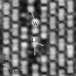
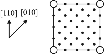
Fig. 7 shows the magnified images of the investigated surface. The rows of the blocks are seen to be situated at varying distances from one another (hereinafter, the distances are measured between corresponding maxima of features). A unit cell is marked with a square box in Fig. 7a. The distances between the adjacent rows of the rectangles are in such structures (‘B’ in Fig. 7a). The adjacent rows designated as ‘A’ are apart ().
A structure with the rows going at apart is presented in Fig. 7b. The lost blocks (‘LB’) that resemble point defects are observed in this image. In addition, a row wedging in between two rows and separating them by an additional distance is seen in the centre of the upper side of the picture (‘W’). The total distance between the wedged off rows becomes .
Hence it may be concluded that the order and some periodicity take place only along the rows—disordering of the structure across the rows is revealed (we often refer to this structure as ).
(a)
 (b)
(b)
The block length can possess two values: Å () and Å (). Distances between equivalent positions of the adjacent short blocks in the rows are . If the long block appears in a row, a divacancy is formed in the adjacent row to restore the checkerboard order of blocks. Fig. 7a illustrates this peculiarity. The long block is marked as ‘L’, the divacancy arisen in the adjacent row is lettered by ‘V’. In addition, the long blocks were found to have one more peculiarity. They have extra maxima in their central regions. The maxima are not so pronounced as the main ones but nevertheless they are quite recognizable in the pictures (Fig. 7a).
Fig. 8 presents magnified STM images of the blocks (“short rectangles”). The images obtained in the empty-state (Fig. 8a) and filled-state (Fig. 8b) modes are different. In the empty-state mode, short blocks look like two lines separated by Å (the distance is measured between brightness maxima in each line). It is a maximum measured value which can lessen depending on scanning parameters. Along the rows, each block is formed by two parts. The distance between the brightness maxima of these parts is Å (or some greater depending on scanning parameters). In the filled-state mode, the block division into two structurally identical parts remains. Depending on scanning conditions, each part looks like either bright coupled dashes and blobs (Figs. 3b and 6b) or two links (brightness maxima) of zigzag chains (Fig. 8b). The distances between the maxima are Å along the rows; this value grows with increasing tunneling current.
The presented STM data are interpreted by us as a structure composed by Si ad-dimers and divacancies.
4 Discussion
4.1 Structural model
The above data allow us to bring forward a model of the observed Si(001) surface reconstruction. The model is based on the following assumptions: (i) the outermost surface layer is formed by ad-dimers; (ii) the underlying layer has a structure of ; (iii) every rectangular block consists of ad-dimers and divacancies a number of which controls the block length.

(a)
 (b)
(b)
 (c)
(c)
Fig. 9a shows a schematic drawing of the structure (a unit cell is outlined). This structure is a basic one for the model brought forward. The elementary structural unit is a short rectangle. These blocks form raised rows running vertically (shown by empty circles). Smaller shaded circles show horizontal dimer rows of the lower terrace. The rest black circles show bulk atoms. Each “rectangle” consists of two dimer pairs separated with a dimer vacancy. The structures on the Si(001) surface composed of close ad-dimers are believed to be stable [6, 13] or at least metastable [43]. In our model, a position of the “rectangles” is governed by the location of the dimer rows of the structure of the underlying layer. The rows of blocks are always normal to the dimer rows in the underlying layer to form a correct epiorientation [43]. Every rectangular block is bounded by the dimer rows of the underlying layer from both short sides. Short sides of blocks form non-rebonded steps [3] with the underlying substrate (see Fig. 5b and three vertically running (the very left) rows of “rectangles” in Fig. 7a).
Fig. 9b demonstrates the same model for the case of the long rectangle. This block is formed due to the presence of an additional dimer in the middle of the rectangle. The structure consisting of one dimer is metastable [6, 13], so this type of blocks cannot be dominating in the structure. Each long block is bounded on both short sides by the dimer rows of the underlying terrace, too. The presence of the long rectangle results in the formation of a dimer-vacancy defect in the adjacent row; this is shown in Fig. 9b—the long block is drawn in the middle row, the dimer vacancy is present in the last left row. According to our STM data the surface is disordered in the direction perpendicular to the rows of the blocks. The distances between the neighboring rows may be less than those in the structure. Hence the structure presented in this paper may be classified as one. Fig. 9c demonstrates an example of such structure—the one.
In Fig. 8, the presented structure is superimposed on STM images of the surface. The filled state image (Fig. 8b) reveals dimer buckling in the blocks which is often observed in this mode at some values of sample bias and tunnelling current. Upper atoms of tilted dimers are shown by larger open circles.
(a)
 (b)
(b)
 (c)
(c)
4.2 Comparison of STM and RHEED data
Now we shall explain the observed discrepancy of results obtained by STM and RHEED within the proposed model. Fig. 10 presents a sketch of the reciprocal lattice of . The RHEED patterns obtained in the azimuth correspond to the structure; the patterns observed in the azimuth do not (Fig. 4). The reason of this discrepancy may be understood from the STM filled state image which corresponds to the electron density distribution of electrons paired in covalent bond of a Si–Si dimer. Fig. 11 compares STM images of the same region on one terrace obtained in the empty-state (a) and filled-state (b) modes; inserts show their Fourier transforms, the differences in which for the two STM modes are as follows: in the Fourier transform of the filled state image, reflexes corresponding to the distance of are absent in the and directions, whereas the reflexes corresponding to and are present (it should be noticed that the image itself resembles that of the reconstructed surface). If an empty state image is not available, it might be concluded that the structure is arranged on the surface. An explanation of this observation is simple. Main contribution to the STM image is made by ad-dimers situated on the sides of the “rectangles”, i. e. on tops of the underlying dimer rows. According to calculations made, e. g., in Refs. [44, 45] dimers located in such a way are closer to the STM tip and look in the images brighter than those situated in the troughs. Hence, it may be concluded that the RHEED pattern results from electron diffraction on the extreme dimers of the “rectangles” forming the surface structure.
The latter statement is illustrated by the STM 3-D empty-state topograph shown in Fig. 11c. The extreme dimers located on the sides of the rectangular blocks are seen to be somewhat higher than the other ones of the dimer pairs; they form a superfine relief which turned out to be sufficient to backscatter fast electrons incident on the surface at grazing angles.
4.3 Origin
The Si(001)- structure have formerly been observed and described in a number of publications [4, 5, 6, 7, 10]. Conditions of its formation were different: coper atoms were deposited on silicon surface to form the reconstruction [10], although it is known that Cu atoms are not absorbed on the Si(001) clean surface if the sample temperature is greater than C, and on the contrary Cu desorption from the surface takes place [7, 10]; fast cooling from the annealing temperature of C was applied [4, 5]; samples treated in advance by ion bombardment were annealed and rapidly cooled [6]. The resultant surfaces were mainly explored by STM and low energy electron diffraction (LEED). STM investigations yielded alike results—a basic unit of the reconstruction was a “rectangle”, but the structure of the “rectangles” revealed by different authors was different. In general, an origin of the Si(001)- structure is unclear now.
STM images most resembling our data were reported in Ref. [5]. In that paper, the structure was observed in samples without special treatment by coper: the samples were subjected to annealing at the temperature of C for the oxide film removal. Formation of the reconstruction was explained in that article by the presence of a trace amount of Cu atoms the concentration of which was beyond the Auger electron spectroscopy detection threshold. The STM empty state images of the samples were similar to those presented in the current paper. A very important difference is observed in the filled state images—we observe absolutely different configuration of dimers within the “rectangles”. Nevertheless, the presence of Cu cannot be completely excluded. Some amount of the Cu atoms may come on the surface from the construction materials of the MBE chamber (although there is a circumstance that to some extent contradicts this viewpoint: Cu atoms were not detected in the residual atmosphere of the MBE chamber within the sensitivity limit of the SRS RGA-200 mass spectrometer) or even from the Si wafer. Cu is known to be a poorly controllable impurity and its concentration in the subsurface layers of Si wafers which were not subjected to the gettering process may reach 1015 cm-3. This amount of Cu may appear to be sufficient to give rise to the formation of the defect surface reconstruction. However, the following arguments urge us to doubt about the Cu-based model: (i) undetectable trace amounts of Cu were suggested in Ref. [5], the presence or absence of which is unprovable; (ii) even if the suggestion is true, our STM images give an evidence of a different amount of dimers in the rectangular blocks, so, it is unclear why Cu atoms form different stable configurations on similar surfaces; and (iii) it is hard to explain why Cu atoms cyclically compose and decompose the rectangular blocks during the cyclical thermal treatments of the samples. It applies equally to any other impurity or contamination.
Now we consider a different interpretation of our data. As mentioned above, literature suggests two causes of appearance. The first is an impact of impurity atoms adsorbed on the surface even at trace concentrations. The second is a thermal cycle of the oxide film decomposition and sample cooling. The first model seems to be hardly applicable for explanation of the reported experimental results. According to our data, there are no impurities adsorbed directly on the studied surface: RHEED patterns correspond to a clean Si(001) surface reconstructed in or, at lower temperatures, configuration. Cyclic contaminant desorption at high temperatures (C) and adsorption on sample cooling is unbelievable. Consecutive segregation and desegregation of an undetectable impurity in subsurface layers also does not seem verisimilar.
(a)
 (b)
(b)
 (c)
(c)
The second explanation looks more attractive. It was found in Ref. [46] as a result of the STM studies that the Si(001) surface subjected to the thermal treatment at C which was used for decomposition of the thin ( nm thick) SiO2 films obtained by chemical oxidation contained a high density of vacancy-type defects and their agglomerates as well as individual ad-dimers. So, the initial bricks for the considered surface structure are abundant after the SiO2 decay.
Literature presents a wide experimental material on a different reconstruction of the Si(001) surface——which also arise at the temperatures of C. For example, a review of articles describing different experimental investigations can be found in Refs. [12, 31, 32, 33, 34, 35]. Based on the generalized data, an inference can be made that the structure forms in the interval from 600 to 700∘C. Most likely, at these temperatures an appreciable migration of Si ad-atoms starts on surface. The structure is free of impurities. It irreversibly transits to the one at the temperature greater than C. Ref. [47] demonstrates formation of the Si(001)- structure, also without impurity atoms. In analogy with the above literature data, formation of the reconstruction may be expected as a result of low-temperature annealing and/or further quenching. The standard annealing temperature for obtaining structure is known to be in the interval from 1200 to 1250∘C. At these temperatures in UHV ambient not only oxide film removal from the surface takes place, but also silicon evaporation and carbon desorption goes on. Unfortunately, we have not got a technical opportunity to carry out such a high-temperature annealing in our instrument. Treatment at 925∘C that we apply likely does not result in substantial evaporation of Si atoms from the surface, and C atoms, if any, may diffuse into subsurface layers. As a result, a great amount of ad-dimers arise on the surface, like it happens in the process described in Ref. [46]. Formation processes of the and structures are different. arise during the high-temperature annealing and ad-atoms of the uppermost layer do not need to migrate and be embedded into the lattice to form this reconstruction. On the contrary, appears during sample cooling, at rather low temperatures, and at the moment of a prior annealing the uppermost layer consists of abundant ad-atoms. On cooling the ad-dimers have to migrate along the surface and be build in the lattice. A number of competing sinks may exist on the surface (steps, vacancies, etc.), but high cooling rate may impede ad-atom annihilation slowing their migration to sinks and in such way creating supersaturation and favoring 2-D islanding, and freezing a high-order reconstruction.
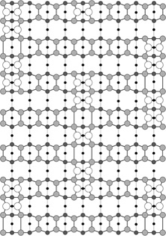
The following scenario may be proposed to describe the structure formation. A large number of ad-dimers remains on the surface during the sample annealing after the oxide film removal. They form the uppermost layer of the structure. The underlying layer is reconstructed. Ad-dimers are mobile and can form different complexes (islands). Calculations show that the most energetically favorable island configurations are single dimer on a row in non-epitaxial orientation [43, 45, 48, 49] (Fig. 5b), complexes of two dimers (pairs of dimers) in epi-orientation (metastable [43]) and two dimers on a row in non-epitaxial orientation separated by a divacancy, and tripple-dimer epi-islands considered as critical epinuclei [43]. These mobile dimers and complexes migrate in the stress field of the structure. The sinks for ad-dimers are (A) steps, (B) vacancy defects of the underlying reconstructed layer, and (C) “fastening” them to the surface as a structure. The main sinks at high temperatures are A and B. As the sample is cooled, the C sink becomes dominating. Ad-dimers on the Si(001)- surface are known to tend to form dimer rows [50]. In this case such rows are formed by metastable dimer pairs gathered in the “rectangles”. The “rectangles” are ordered with a period of 8 translations in the rows. The ordering is likely controlled by the structure of the underlying layer and interaction of the stress fields arising around each “rectangle”. Effect of the underlying layer is that the “rectangle” position on the surface relative to its dimer rows is strictly defined: dimers of the “rectangle” edges must be placed on tops of the rows. Interaction of the stress fields initially arranges the “rectangles” within the rows (Fig. 12a), then it arranges adjacent rows with respect to one another (Fig. 12b). The resultant ordered structure is shown in Fig. 12c. The described behaviour of “rectangles” can be derived from the STM images presented in the previous sections. In addition, investigation of appearance of the RHEED patterns allowed us to conclude that the process of dimer ordering in the structure is gradual: the pattern reflexes appearing on transition from to reach maximum brightness gradually; it means that the structure does not arise instantly throughout the sample surface, but originally form some nuclei (“standalone rectangles” like those in Fig. 5a) on which mobile ad-dimers crystallize in the ordered surface configuration.
4.4 Stability
A source of stability of the Si(001) surface configuration composed by ad-dimers gathered in the rectangular islands has not been found to date. Some of possible sources of stabilization of structures with high-order periodicity were considered in Refs. [31, 47, 51, 52, 53]. One of likely reasons of high-order structure formation might be a non-uniformity of the stress field distribution on a sample surface and dependance of this distribution on such factors as process temperature, sample cooling rate, specimen geometry and a way of sample fastening to a holder, presence of impurity atoms on and under the surface. In this wise, it is clear only that ad-dimers form “rectangles” which are energetically favorable at temperature conditions of the experiments.
In this connection, a guide for further consideration could be found in Ref. [43] where an issue of the critical epinucleus—or the smallest island which unreconstructs the surface and whose probability of growth is greater than likelihood of decay—on the reconstructed Si(001) was theoretically investigated. First-principle calculations showed that dimer pairs in epi-orientation are metastable and the epinucleus consists of tripple dimers [43]. Unfortunately, we failed to observe tripple-dimer islands in our experiments, and calculations were limited to three dimers in the cited article. Some formations smaller than “rectangles” sometimes are observed in images of the rarified structures (Fig. 5a) but they are likely single dimers (Fig. 5b) and dimer pairs. We believe that the short “rectangles” we deal with in this article might be considered as epinuclei for the structure because, although they show no tendency to grow themselves, they are both seeds and structural units for formation of larger islands such as chains (Fig. 5a), grouped chains (Fig. 2a) and complete ares (Fig. 6). From other hand, they also do not tend to decay or annihilate even on as powerful sinks as steps (Fig. 5a). Thus, we conclude that the stability of such epi-islands as dimer pair-vacancy-pair (short “rectangles”, Fig. 9a,c) is the highest. Less probable (stable) configuration is pair-vacancy-dimer-vacancy-pair (long “rectangle”, Fig. 9b). We think its less stability is due to presence of a single epi-oriented dimer in the centre. That is why long “rectangles” are much less spread on the Si(001) surface than the short ones and entire structure stabilization in the presence of the long “rectangles” requires appearance of additional dimer vacancies between “rectangles” in adjacent rows in the vicinity of the long blocks.
5 Conclusion
In summary, it may be concluded that the Si(001) surface prepared under the conditions of the UHV MBE chamber in a standard wafer preparation cycle has reconstruction which is partly ordered only in one direction. Two types of unit blocks form the rows running along and axes. When the long block disturbs the order in a row a dimer-vacancy defect appears in the adjacent row in the vicinity of the long block to restore the checker-board order of blocks in the neighboring rows.
Discrepancy of RHEED patterns and STM images was detected. According to RHEED data, and structures can form the Si(001) surface during sample treatment. STM studies of the same samples at room temperature show that a high-order reconstruction exists on the Si(001) surface; simultaneously, the underlying layer is reconstructed in the areas free of the structure. A fraction of the surface area covered by the structure decreases as the sample cooling rate is reduced. RHEED patterns corresponding to the reconstruction arise at C in the process of sample cooling after annealing. The reconstruction is reversible: the structure turns into the one at C in the process of the repeated sample heating, the structure appears on the surface again at the same temperature during recurring cooling.
A model of the structure based on epi-oriented ad-dimer complexes has been presented. Ordering of the ad-dimer complexes likely arise due to interaction of the stress fiends produced by them. The discrepancy of the STM and RHEED data has been explained within the proposed model: the structure revealed by STM has been evidenced to manifest itself as the one in the RHEED patterns.
Probable causes of the reconstructed Si(001) surface formation have been discussed. A combination of low temperature of sample annealing and high rate of its cooling may be considered as one of the most plausible factors responsible for its appearance. The structural units of the studied reconstruction are supposed to be its critical epinuclei.
6 Acknowledgements
The research was supported by the Science and Innovations Agency of RF under the State Contract No. 02.513.11.3130 and the Education Agency of RF under the State Contract No. 2367.
References
- [1] V. A. Yuryev, L. V. Arapkina, V. A. Chapnin, V. P. Kalinushkin, N. V. Kiryanova, O. V. Uvarov, K. V. Chizh, L. A. Krylova, R. O. Stepanov, O. O. Zaytsev, Development of physical and technological basis of the controllable formation of densely packed Ge nanocluster arrays on the silicon (100) surface by means of ultrahigh vacuum molecular beam epitaxy, Report on Research Project 2007-3-1.3-25-01-303 of the Science and Innovations Agency of the Russian Federation, A. M. Prokhorov General Physics Institute of the Russian Academy of Sciences, Moscow, Russia, VNITC State Reg. No. 0220.0 802501 (2007).
- [2] R. J. Hamers, R. M. Tromp, J. E. Demuth, Scanning tunneling microscopy of Si(001), Phys. Rev. B 34 (1986) 5343.
- [3] D. J. Chadi, Stabilities of single-layer and bilayer steps on Si(001) surfaces, Phys. Rev. Lett. 59 (1987) 1691.
- [4] X. Hu, Z. Lin, Hydrogen adsorption induced phase transitions on Si(100)-: temperature dependence studied by LEED, Appl. Surf. Sci. 90 (1995) 111.
- [5] P. W. Murray, R. Lindsay, F. M. Leibsle, P. L. Wincott, G. Thornton, Direct observation of the defect structure on Si(001) using scanning tunnelling microscopy, Phys. Rev. B 54 (1996) 13468.
- [6] T. Kubo, T. Agura, N. Takagi, M. Nishijima, Investigation on the surface electronic states of the Si(001) and surfaces: An electron energy loss spectroscopy study, Jpn. J. Appl. Phys. 36 (1997) L975.
- [7] H. Iton, T. Ann, T. Kawasaki, T. Ichinokawa, Surface structures and growth mode of Cu/Si(100) surfaces by scanning tunnelling microscopy, Surf. Rev. Lett. 5 (1998) 747.
- [8] J.-Y. Koo, J.-Y. Yi, C. Hwang, D.-H. Kim, G. Lee, S. Lee, Basic structure of the kinked monatomic steps on the Si(001) surface, Phys. Rev. B 57 (1998) 8782.
- [9] K. Hata, S. Yasuda, H. Shigekawa, Reinterpretation of the scanning tunnelling microscopy images of Si(100)- dimers, Phys. Rev. B 60 (1999) 8164.
- [10] B. Z. Liu, M. V. Katkov, J. Nogami, An STM study of Cu on Si(001) in the structure, Surf. Sci. 453 (2000) 137.
- [11] H. Okada, Y. Fujimoto, K. Endo, K. Hirose, Y. Mori, Detailed analysis of scanning tunneling microscopy images of the Si(001) reconstructed surface with buckled dimers, Phys. Rev. B 63 (2001) 195324.
- [12] A. Goryachko, P. V. Melnik, N. G. Nakhodkin, T. V. Afanasjeva, I. F. Koval, New features of the Si(100)- reconstruction observed with STM: suggestion of the structure with lowered symmetry, Surf. Sci. 497 (2002) 47.
- [13] H. W. Liu, H. Q. Yang, H. M. Guo, Y. L. Wang, X. Lin, S. J. Pang, H. J. Gao, Patterns formed on the dimer vacancy array of Si(100) by self-assembly, Nanotechnol. 13 (2002) 729.
- [14] L. V. Arapkina, V. M. Shevlyuga, V. A. Yuryev, Structure and peculiarities of the -type Si(001) surface prepared in a molecular beam epitaxy chamber: A scanning tunneling microscopy study, JETP Lett. 87 (2008) 215, arXiv:0908.1346.
- [15] L. V. Arapkina, K. V. Chizh, V. M. Shevlyuga, V. A. Yuryev, The controllable formation of densely packed arrays of Ge nanoclusters on the silicon (001) surface by means of ultrahigh vacuum molecular beam epitaxy, in: A. L. Aseev, A. V. Dvurechenskiĭ (Eds.), Russian Conference on Actual Problems of Semiconductor Photoelectronics (“Photonics-2008”), A. V. Rzhanov Institute of Semiconductor Physics of Siberian Brunch of the Russian Academy of Sciences, Novosibirsk, Russia, 2008, p. 48.
- [16] L. V. Arapkina, V. A. Yuryev, V. M. Shevlyuga, STM and RHEED investigations of the defect structure on Si(001), in: 25-th International Conference on Defects in Semiconductors (ICDS-25), St. Petersburg, Russia, 2009, p. 348.
- [17] L. V. Arapkina, V. A. Yuryev, K. V. Chizh, V. A. Chapnin, Nucleation and growth of Ge hut clusters on the Si(001) surface at low temperatures, in: Proc. XIV Int. Symp. “Nanophysics and nanoelectronics”, Vol. 2, Inst. Microstruct. Phys. RAS, Nizhni Novgorod, Russia, 2010, p. 531.
- [18] A. V. Dvurechenskii, V. A. Zinoviev, V. A. Kudryavtsev, J. V. Smagina, Effects of low-energy ion irradiation on Ge/Si heteroepitaxy from molecular beam, JETP Lett. 72 (3) (2000) 131.
- [19] A. V. Dvurechenskii, V. A. Zinoviev, J. V. Smagina, Self-organization of an ensemble of Ge nanoclusters upon pulsed irradiation with low-energy ions during heteroepitaxy on Si, JETP Lett. 74 (2001) 267.
- [20] A. V. Dvurechenskii, V. A. Zinovyev, V. A. Kudryavtsev, J. V. Smagina, P. L. Novikov, S. A. Teys, Ion-beam assisted surface islanding during Ge MBE on Si, Phys. Low-Dim. Struct. 1/2 (2002) 303.
- [21] A. V. Dvurechenskii, J. V. Smagina, V. A. Zinoviev, V. A. Armbrister, V. A. Volodin, M. D. Efremov, Elemental composition of nanoclusters formed by pulsed irradiation with low-energy ions during Ge/Si epitaxy, JETP Lett. 79 (7) (2004) 333.
- [22] A. V. Dvurechenskii, J. V. Smagina, V. A. Zinovyev, S. A. Teys, A. K. Gutakovskii, Modification of growth mode of Ge on Si by pulsed low-energy ion-beam irradiation, Int. J. Nanoscience 3 (1/2) (2004) 19.
- [23] A. V. Dvurechenskii, J. V. Smagina, R. Groetzschel, V. A. Zinoviev, V. A. Armbrister, P. L. Novikov, S. A. Teys, A. K. Gutakovskii, Ge/Si quantum dot nanostructures grown with low-energy ion beam-epitaxy, Surf. Coat. Technol. 196 (1–3) (2005) 25.
- [24] A. V. Dvurechenskii, J. V. Smagina, V. A. Armbrister, V. A. Zinovyev, P. L. Novikov, S. A. Teys, R. Groetzschel, Ge/Si nanostructures with quantum dots grown by ion-beam-assisted heteroepitaxy, in: B. Joyce, P. Kelires, A. Naumovets, D. Vvedensky (Eds.), Quantum Dots: Fundamentals, Applications and Frontiers, Kluwer Academic Publishers, Netherlands, 2005, p. 135.
- [25] N. P. Stepina, A. V. Dvurechenskii, V. A. Armbrister, J. V. Smagina, V. A. Volodin, A. V. Nenashev, J. P. Leito, M. C. do Carmo, N. A. Sobolev, MBE growth of Ge/Si quantum dots upon low-energy pulsed ion irradiation, Thin Solid Films 517 (2008) 309.
- [26] J. V. Smagina, V. A. Zinovyev, A. V. Nenashev, A. V. Dvurechenskiĭ, V. A. Armbrister, S. A. Teys, Self-assembly of germanium islands under pulsed irradiation by a low-energy ion beam during heteroepitaxy of Ge/Si(100) structures, JETP 106 (2008) 517.
- [27] L. V. Arapkina, V. A. Yuryev, Classification of Ge hut clusters in arrays formed by molecular beam epitaxy at low temperatures on the Si(001) surface, Phys.-Usp. 53 (3) (2010) 279, arXiv:0907.4770.
- [28] L. V. Arapkina, V. A. Yuryev, Atomic structure of Ge quantum dots on the Si(001) surface, JETP Lett. 91 (6) (2010) 281, arXiv:0908.0883.
- [29] L. V. Arapkina, V. A. Yuryev, Nucleation of Ge quantum dots on the Si(001) surface, Phys. Rev. B 82 (2010), to be published, arXiv:0907.4665.
- [30] V. A. Yuryev, L. V. Arapkina, Defects of Ge quantum dot arrays on the Si(001) surface, Physica B 404 (2009) 4719, arXiv:0908.0841.
- [31] K. Miki, K. Sakamoto, T. Sakamoto, Is the reconstruction of Si(001) associated with the presence of carbon?, Appl. Phys. Lett. 71 (1997) 3266.
- [32] R. I. G. Uhrberg, J. E. Northrup, D. K. Biegelsen, R. D. Bringans, L.-E. Swartz, Atomic structure of the metastable reconstruction of Si(100), Phys. Rev. B 46 (1992) 10251.
- [33] Z. Zhang, M. A. Kulakov, B. Bullemer, Scanning tunnelling microscopy study of Si(100)-c(4x4) structure formation by annealing of Si epitaxial films, Surf. Sci. 69 (1996) 369.
- [34] Z. Zhang, M. A. Kulakov, B. Bullemer, Surface morphology and reconstructions of ultra thin Si films growth by solid-phase epitaxy, Thin Solid Films 294 (1997) 88.
- [35] F. K. Men, J. L. Erskine, Metastable oxygen-induced ordered structure on the Si(001) surface, Phys. Rev. B 50 (1994) 11200.
- [36] K. N. Eltsov, Ultrahigh vacuum scanning tunnelling microscope STM GPI-300, http://surface.gpi.ru/papers/gpi300e.pdf.
- [37] K. N. Eltsov, A. N. Klimov, A. N. Kosyakov, O. V. Obyedkov, V. M. Shevlyuga, V. Y. Yurov, Ultrahigh vacuum scanning funnelling microscope GPI-300, in: V. I. Konov, K. N. Eltsov (Eds.), Chemical state and atomic structure of fcc metal surfaces in chemical reaction with halogens, Vol. 59 of Proc. General Phys. Inst., Nauka, Moscow, Russia, 2003, p. 45.
- [38] V. Y. Yurov, A. N. Klimov, Scanning tunneling microscope calibration and reconstruction of real image—drift and slope elimination, Rev. Sci. Instrum. 65 (1994) 1551.
- [39] I. V. Kiryushina, Processes of liquid chemical preparation of silicon wafers in the VLSI production with sub-micrometer design rules, Ph.D. thesis, JSC Mikron, Zelenograd, Moscow, Russia, in Russian (2003).
- [40] K. N. Eltsov, V. M. Shevlyuga, V. Y. Yurov, A. V. Kvit, M. S. Kogan, Sharp tungsten tips prepared for STM study of deep nanostructures in UHV, Phys. Low-Dim. Struct. 9/10 (1996) 7.
- [41] I. Horcas, R. Fernandez, J. M. Gomez-Rodriguez, J. Colchero, J. Gomez-Herrero, A. M. Baro, WSxM: A software for scanning probe microscopy and a tool for nanotechnology, Rev. Sci. Instrum. 78 (2007) 013705.
- [42] J. E. Mahan, K. M. Geib, G. Y. Robinson, R. G. Long, A review of the geometrical fundamentals of reflection high-energy electron diffraction with application to silicon surfaces, J. Vac. Sci. Technol. A 8 (1990) 3692.
- [43] R. G. S. Pala, F. Liu, Critical epinucleation on reconstructed surfaces and first-principle calculation of homonucleation on Si(001), Phys. Rev. Lett. 95 (2005) 136106.
- [44] Z. Zhang, F. Wu, H. J. Zandvliet, B. Poelsema, H. Metiu, M. G. Lagally, Energetics and dynamics of Si ad-dimers on Si(001), Phys. Rev. Lett. 74 (1995) 3644.
- [45] G. Brocks, P. J. Kelly, R. Car, The energetics of adatoms on the Si(100) surface, Surf. Sci. 269/270 (1992) 860.
- [46] A. Ney, J. J. Schulz, C. Pampuch, L. Peripelittchenko, R. Koch, Atomic structure of low temperature prepared Si(001) substrates, Surf. Sci. 520 (2002) L633.
- [47] T. Aruga, Y. Murata, Ordered-defect model for Si(001), Phys. Rev. B 34 (1986) 5654.
- [48] Z. Zhang, H. Metiu, The self-organization of Si atoms adsorbed on a Si(100) surface: an atomic level kinetic model, Surf. Sci. Lett. 292 (1993) L781.
- [49] K. Terakura, T. Yamasaki, T. Uba, I. Stich, Atomic and molecular processes on Si(001) and Si(111) surfaces, Surf. Sci. 386 (1997) 207.
- [50] Y.-W. Mo, B. S. Swartzentruber, R. Kariotis, M. B. Webb, M. G. Lagally, Growth and equilibrium structures in the epitaxy of Si on Si(001), Phys. Rev. Lett. 63 (1989) 2393.
- [51] H. Q. Yang, C. X. Zhu, J. N. Gao, Z. Q. Xue, S. J. Pang, Large area dimer vacancy array on the Si(100) surface studied by scanning tunneling microscope, Surf. Sci. 412/413 (1998) 236.
- [52] A. Natori, R. Nishiyama, H. Yasunaga, Stability of ordered missing-dimer structures and the ordering dynamics on Si(001), Surf. Sci. 397 (1998) 71.
- [53] Y. F. Zhao, H. Q. Yang, S. J. Pang, Si(100) reconstruction formed in a highly nonequilibrium process, Phys. Rev. B 62 (2000) R7715.