External Bias Dependent Direct To Indirect Bandgap Transition in Graphene Nanoribbon
Graphene, the two dimensional allotrope of carbon, has drawn an enormous amount of attention in the literature after its first isolation on an oxide substrate [1, 2]. Apart from the theoretical physics point of view [3, 4], graphene has emerged as a possible candidate for different electronic devices including field effect transistors [5]-[8]. However, the small bandgap of graphene reduces the controllability of such devices and thus limits its widespread applications. Graphene Nanoribbon (GNR), on the other hand, a quasi-one dimensional strip of graphene, has been shown to provide a significant bandgap [9]-[12] and hence is being considered as a channel material in field effect transistors [13]-[15].
More recently, it has been theoretically shown that the bandgap of a graphene nanoribbon can be tuned significantly by the application of an external field along the width of the ribbon [16, 17, 18] and at sufficiently large field, it is also possible to collapse the gap of the ribbon. In this work, we extend this result in a more generic way for both semiconducting and metallic Armchair Graphene NanoRibbon (A-GNR) and demonstrate that not only the magnitude of the bandgap, but the whole electronic structure of the nanoribbon can be altered significantly depending on the magnitude and polarity of the external bias. In particular, we will show that it is possible to obtain a bias dependent direct to indirect bandgap transition in such a nanoribbon. This kind of control over the electronic structure by the application of an external bias opens up the possibility of new device applications.
A schematic of the setup that we consider in this work is shown in Fig. 1, where an Armchair Graphene NanoRibbon A-GNR of width is sandwiched between a left gate (GL) and a right gate (GR). There is a third contact which keeps the chemical potential of the A-GNR at zero. In this work, we will primarily focus on semiconducting nanoribbons, i.e., the number of dimers () along the width, is of the form and . Note that, gives rise to metallic nanoribbons [11, 12] and is briefly analyzed in this work. The gate terminal in each gate stack is separated from the GNR by a dielectric. We assume the Equivalent Oxide Thickness (EOT) of the gate dielectric to be 1nm. The interfaces between the GNR and the gate dielectric are assumed to be perfect, hence the electronic structure of the GNR is not altered significantly. The gate dielectric confines the electrons and holes in the GNR along the direction, however the component of the states can be obtained using longitudinal wave vector . The work function of the gate metal is assumed to be such that a zero flatband voltage is obtained. The external biases and at the left and the right gates respectively can be varied independently. The application of an external bias changes the potential energy inside the GNR, altering the electronic structure.
We now provide the details of the calculation procedure used to investigate the effect of external bias on an A-GNR. The self-consistent electronic structure of the A-GNR is determined by using tight binding method ([19, 20]) coupled with the Poisson equation. Taking the left edge of the GNR at and the plane of the GNR as , the charge density is given by , where is the electronic charge and is obtained as the difference between the hole [] and electron [] density as
| (1) |
where is the Fermi-Dirac probability at temperature . Here goes over the whole first Brillouin Zone, and are the valence and conduction band indices respectively. The chemical potential , set by the contact , is taken to zero. is the energy eigenvalue of the state obtained from the tight binding bandstructure taking only orbital into account, with an intra-layer overlap integral, = 0.129 between two nearest carbon atoms and the intra-layer hopping as 3.033eV [19]. Note that, the results obtained from the nearest neighbor calculation are in close agreement with simulation that take into account coupling terms up to the third nearest neighbor (see supporting information). To obtain the wavefunction , we assume normalized Gaussian orbital as the basis function, where the parameter of the basis function is fitted using the parameter . The wavefunctions are set to zero at the dielectric interfaces indicating an infinite potential barrier. Once self-consistency is achieved between the bandstructure calculation and the Poisson equation for a given gate bias, the energy eigenvalues at different points correspond to the electronic structure of the A-GNR.
We take an A-GNR with (nm) and consider three
representative bias conditions, namely, (i) , (ii) , and (iii) , . We now present the results
in these three cases as shown in Fig.
2-4.
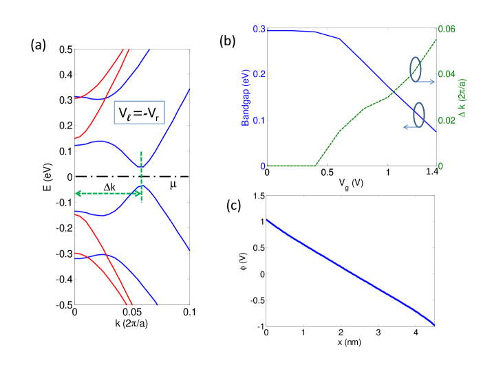
Case (i): In this case, the two gate voltages are anti-symmetric in nature, i.e., . We observe a significant reduction of bandgap in Fig. 2(a) and (b) with an increase in , and this has also been predicted in [17, 18]. It is observed that at sufficiently large , both the conduction and valence band edges shift from , giving a ‘Mexican Hat’ shape around . Fig. 2(b) clearly shows a threshold like behavior of the bandgap change [17], and as the band edges shift from (non-zero ), the bandgap starts decreasing significantly with bias. However, the particle-hole symmetry is almost conserved (the small asymmetry in Fig. 2(a) is due to the non-zero overlap assumed between two nearest neighbor carbon atoms in the honeycomb lattice) and hence the bandgap continues to remain direct in nature, at any bias condition. Note that, the anti-symmetric bias condition forces the GNR to retain its charge neutral condition with similar electron and hole density, keeping the total effective charge density very low. , dictated by the Poisson’s equation, thus remains almost linear (uniform field) along , as shown in Fig. 2(c). Note that bias dependent bandgaps match very well with one of the previously published reports based on non-selfconsistent calculations [18] and this linearity of along the width of the nanoribbon is the reason of this unexpected close match.
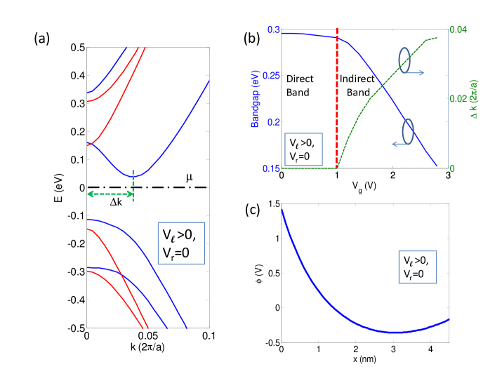
Case (ii): In this case, the left gate is kept at positive bias, keeping the right gate grounded and the results are shown in Fig. 3(a)-(c). The bandstructure shows a dramatic change as compared with case (i). With an increase in , the conduction band minimum shifts from , giving rise to a ‘Mexican Hat’ shape around . However, the valence band maximum continues to remain at , irrespective of . Thus, at any for which , the GNR has an indirect bandgap. The direct and indirect bandgap regions are indicated in Fig. 3(b). The magnitude of the bandgap continues to show a threshold-like behavior as before, with an increased sensitivity of bandgap when the system becomes indirect. Note that, the spatial distribution of along the width of the nanoribbon is severely non-linear (non-uniform field) to support the increased electron density inside the GNR that arises due to the conduction band edge moving closer to the chemical potential. We will later point out that it is this strong non-linearity of that causes such a direct to indirect bandgap transition.
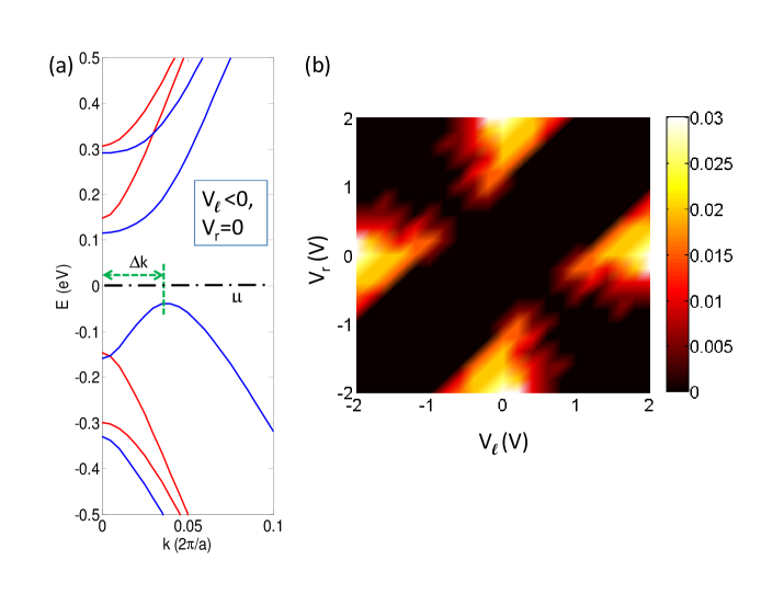
Case (iii): A similar case like (ii) can be constructed where the left gate is at negative bias, with the right gate grounded. The bandstructure in such a scenario is shown in Fig. 4(a) where the conduction band minimum continues to remain at , and the valence band maximum shifts away from , depending on the external bias. In this case, the valence band edge moves closer to the chemical potential resulting in a relative increase in the hole density.
Note that the corrections due to the second and the third nearest neighbor interactions contribute at relatively large values of , away from the zone center [21]. However, the band edge shift () from the zone center (), in all the above scenarios, are small () compared to the size of the Brillouin zone. Hence, the calculations with nearest neighbor interactions are accurate enough to predict such direct to indirect bandgap transition.
In Fig. 4(b), we generalize this result and show the
transition from direct to indirect bandgap in the (,)
space. We compute the absolute difference of the values of the
conduction band minimum and the valence band maximum for any
arbitrary combination of and . This is plotted as a
function of (,) in Fig. 4(b). A zero value
(dark color) indicates direct bandgap, whereas a non-zero value
(lighter color) represents indirect bandgap region. We clearly
observe that in the (,) space, there are symmetric pockets
of indirect bandgap regions, with the chosen cases (ii and iii) are
the most favorable conditions to obtain such a bandgap transition.
In the case of a metallic A-GNR, it is interesting to note that an asymmetric external electric field along the width opens a small bandgap at the zone center. Fig. 5(a) shows a direct bandgap of meV for a metallic A-GNR with under a bias of 2.8V at the left gate, while grounding the other. However, as shown in Fig. 5(b), at larger bias, this bandgap tends to become indirect accompanied with a reduction in its magnitude. We do not observe such an effect in the case of anti-symmetric bias condition, in agreement with [17].
The external bias dependent direct to indirect bandgap transition,
coupled with the change in magnitude of the bandgap can have
significant effects in phenomena including band-to-band tunneling,
electron-phonon interaction and optical properties. Such an external
bias dependent tailoring of the electronic structure can provide us
with the possibility of a wide variety of fascinating electronic and
optoelectronic device applications.
Now, to get more insights, we present a theoretical analysis of the phenomenon by starting from the Dirac equation [11, 12, 17]. We write the low energy states in terms of smoothly varying envelop . and have components on the and sublattices in the honeycomb lattice with and nm [17]. By making the replacement in the Dirac Hamiltonian [12], we can write where the Hamiltonian () for the nanoribbon is given as
| (2) |
with . Here, are the Pauli matrices and m/s. To keep the analysis simple, we assume the intra-layer coupling parameter to be zero. The armchair boundary condition with ideal edges forces
| (3) |
and
| (4) |
Now, we give a simple argument to show why we observe a direct to indirect bandgap transition in setup (ii) and (iii), whereas setup (i) provides direct bandgap independent of external bias. If we write the full Hamiltonian by discretization of space along , we find,
| (5) |
which is equal to zero in case (i) and this holds good for any . This is due to the anti-symmetric nature of the external bias and hence of about the mid point of the nanoribbon. Now, using the fact that the sum of the eigenvalues equals the trace of , this condition forces the sum of the energy eigenvalues at any to be zero. Thus the conduction band and valence band remain symmetric about , forcing the bandgap to be direct at any external gate bias. However, in cases (ii) and (iii), the asymmetric gate biases introduce consequent asymmetry in the spatial distribution of and hence force to become nonzero, allowing asymmetry in the conduction and the valence bands. This manifests as a bandgap transition in the nanoribbon.
We now provide an independent numerical method derived from Eq. 2 to re-calculate the bias dependent electronic structure and verify the trend of direct to indirect bandgap transition obtained from tight binding calculations. To do this, We rewrite as [17]
| (6) |
where
| (7) |
Since, in general, does not commute for two different , we can write the solutions in terms of Magnus series [22, 23]:
| (8) |
where . is the term in the Magnus series with the first three terms are given as
| (9) | |||||
Using Eqs. 3, 4 and 8, we obtain
| (10) |
To get non-trivial solutions for , we obtain
| (11) |
For a given , the set of values of satisfying Eq. 11 gives the required energy eigenvalues, which can be found numerically. We have verified that the results obtained using this method show a direct to indirect bandgap transition in setup (ii) and (iii) whereas the GNR continues to remain a direct bandgap semiconductor in case (i).
As a special case, commutes for two different for and hence = becomes zero for . Hence, we can readily observe from Eq. 11 that as long as , we do not have any change in the energy eigenvalues at for any arbitrary . This is why we should not expect any change in = for any external bias as long as . Note that, in reality, as shown in Fig. 2(a), we do see a small change in = under gate bias, which arises from non-zero overlap parameter . However, in case (ii) and (iii), nonzero introduces a bias dependent upward or downward shift in the value depending on the polarity of the terminal bias.
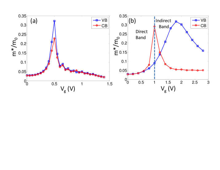
As a final comment, we extract the effective mass values at the conduction band minimum and the valence band maximum for case (i) and (ii) using the relationship obtained from self-consistent tight binding calculations. The results are shown in Fig. 6(a)-(b). In both the cases, we observe strong non-monotonic behavior of the effective mass values, both for the electrons and the holes. In case (i) [Fig. 6(a)], the effective mass of the electrons follows that of the holes for both small and large biases. However, at some intermediate gate bias, where the band edges start shifting from , we notice a significant difference in the electron and the hole effective mass values, though both of them strongly peak about that point. A similar behavior is observed in the electron effective mass in case (ii) [Fig. 6(b)], which sharply peaks around the direct to indirect band transition point indicating a “flattening” of the conduction band edge when it moves away from . However, we do not observe any such sharp peak in the hole effective mass around the bandgap transition point. This sharp notch like behavior of the effective masses (with almost an order of magnitude change) is a unique feature of the influence of the external field on the electronic structure of A-GNR where one can selectively “slow down” the carriers by choosing the appropriate external bias condition.
To conclude, using a self-consistent tight binding calculation, we have demonstrated that it is possible to change the bandgap of an semiconducting A-GNR from direct to indirect by adjusting the external biases at the left and the right gate, opening up the possibility of new device applications. Such a direct to indirect bandgap transition has been explained, both qualitatively as well as quantitatively, by starting from Dirac equation, to support the findings obtained from tight-binding calculations. Finally, the external bias dependent carrier effective masses have been shown to have non-monotonic sharp behavior around the direct to indirect bandgap transition point.
Acknowledgement: K. Majumdar and N. Bhat would like to thank the Ministry of Communication and Information Technology, Government of India, and the Department of Science and Technology, Government of India, for their support.
References
- [1] Novoselov, K. S.; et al. Electric Field Effect in Atomically Thin Carbon Films. Science 2004, 306, 666-669.
- [2] Novoselov, K. S.; et al. Two-dimensional gas of massless Dirac fermions in graphene. Nature 2005, 438, 197.
- [3] Geim, A. K.; et al. The Rise of Graphene. Nat. Mat. 2007, 6, 183.
- [4] Novoselov, K. S.; et al. Unconventional quantum Hall effect and Berry’s phase of in bilayer graphene. Nat. Phys. 2006, 2, 177.
- [5] Lemme, M. C.; et al. A Graphene Field-Effect Device. IEEE Elec. Dev. Lett. 2007, 28, 282.
- [6] Oostinga, J. B.; et al. Gate-induced insulating state in bilayer graphene devices. Nat. Mat. 2008, 7, 151.
- [7] Chen, J. H.; et al. Intrinsic and extrinsic performance limits of graphene devices on SiO2. Nat. Nano. 2008, 3, 206.
- [8] Lin, Y. M.; et al. 100-GHz Transistors from Wafer-Scale Epitaxial Graphene. Science 2010, 327, 662.
- [9] Nakada, K.; et al. Edge state in graphene ribbons: Nanometer size effect and edge shape dependence. Phys. Rev. B 1996, 54, 17954.
- [10] Son, Y. W.; Energy Gaps in Graphene Nanoribbons. Phys. Rev. Lett. 2006, 97, 216803.
- [11] Brey, L.; et al. Edge states and the quantized Hall effect in graphene. Phys. Rev. B 2006, 73, 195408.
- [12] Brey, L.; et al. Electronic states of graphene nanoribbons studied with the Dirac equation. Phys. Rev. B 2006, 73, 235411.
- [13] Obradovic, B.; et al. Analysis of graphene nanoribbons as a channel material for field-effect transistors. Appl. Phys Lett. 2006, 88, 142102.
- [14] Yan, Q.; et al. Intrinsic Current-Voltage Characteristics of Graphene Nanoribbon Transistors and Effect of Edge Doping. Nano Lett. 2007, 7, 1469.
- [15] Rojas, F. M.; et al. Performance limits of graphene-ribbon field-effect transistors. Phys. Rev. B 2008, 77, 045301.
- [16] Son, Y. W.; et al. Half-Metallic Graphene Nanoribbons. Nature 2006 444, 347.
- [17] Novikov, D. S.; Transverse Field Effect in Graphene Ribbons. Phys. Rev. Lett. 2007, 99, 056802.
- [18] Raza, H.; et al. Armchair graphene nanoribbons: Electronic structure and electric-field modulation. Phys. Rev. B 2008, 77, 245434.
- [19] Saito, R.; et al. “Physical Properties of Carbon Nanotubes,” World Scientific Publishing, 1998.
- [20] Slater, J.C.; et al. Simplified LCAO Method for the Peroidic Potential Problem. Phys. Rev. 1954, 94, 1498.
- [21] Reich, S.; et al. Tight-binding description of graphene. Phys. Rev. B 2002, 66, 035412.
- [22] Magnus, W.; On the exponential solution of differential equations for a linear operator. Comm. Pure and Appl. Math. 1954, VII: 649.
- [23] Blanes, S.; et. al. Magnus and Fer expansions for matrix differential equations: The convergence problem. Phys. Rep., 2009, 470, 151.