Piezoconductivity of gated suspended graphene
Abstract
We investigate the conductivity of graphene sheet deformed over a gate. The effect of the deformation on the conductivity is twofold: The lattice distortion can be represented as pseudovector potential in the Dirac equation formalism, whereas the gate causes inhomogeneous density redistribution. We use the elasticity theory to find the profile of the graphene sheet and then evaluate the conductivity by means of the transfer matrix approach. We find that the two effects provide functionally different contributions to the conductivity. For small deformations and not too high residual stress the correction due to the charge redistribution dominates and leads to the enhancement of the conductivity. For stronger deformations, the effect of the lattice distortion becomes more important and eventually leads to the suppression of the conductivity. We consider homogeneous as well as local deformation. We also suggest that the effect of the charge redistribution can be best measured in a setup containing two gates, one fixing the overall charge density and another one deforming graphene locally.
pacs:
73.22.Pr., 73.23.Ad., 73.50.Dn, 46.70.DeI Introduction
Graphene is a novel material with highly unusual electron properties, related to the Dirac form of its energy spectrum at low energies, and demonstrated in many seminal experiements (for review see BeenakkerR ; CastroNeto ). Experiments on single-layer graphene have been performed on the flakes obtained by exfoliation as well as grown on a substrate.
Graphene also has excellent mechanical properties. Indeed, the elastic properties have been measured on suspended graphene flakes mechanically deposited over a hole by indentation in an atomic force microscope Changgu ; Delftexp ; FrankAFM ; the results showed that graphene is incredibly stiff, with the breaking strength of the order of N/m, the Young modulus of 1 TPa, and possibility to be stretched elastically up to 20. Bending properties have been determined experimentally for several-layer graphene flakes Delftexp and are not yet available for a monolayer. Theoretically, these properties have been predicted from the calculations using the analytical form of the interatomic potential, and from molecular dynamic studies Huang ; Huang2 . Graphene is currently one of the most prospective candidates for high-frequency nanomechanical resonators Bunch ; Chen , with the quality factor and eigenfrequency extracted from measurements to be , MHz for a monolayer, and , MHz for 15nm thick graphite. Quality factor further increases with decreasing temperature. An alternative method to investigate elastic properties of graphene is to put the film on a flexible substrate and deform the substrate grow3 ; Mohiuddin . The strain influences optical phonon spectum Mohiuddin , which has been measured by Raman spectroscopy.
Recent experiments combine mechanical and electrical properties of graphene by measuring conductivity Bolotin1 ; Bolotin2 ; Lau ; suspended of suspended graphene flakes. This is a very promising direction since suspended graphene flakes exhibit much higher mobility than graphene on substrate due to much weaker disorder Bolotin1 ; Bolotin2 . Potentially electrons can produce back-action on the resonator. Graphene resonators are expected to have high sensitivity to mass and prebuilt strain Chen , so that they can be used to ultra-sensitive mass detection.
Suspension of graphene flakes always leads to their deformation, which in turn affects the conduction properties of graphene. Deformation creates inhomogeneous elongation of the lattice constant CastroNetoD ; Katsnelson which locally affects the electron spectrum of graphene. One way to look at the variations of the band structure of the strained graphene is to perform density functional calculations CastroNetomol . Alternatively, the variation of the lattice constant can be represented at the level of Dirac equation in the form of pseudomagnetic fields Ando . Ref. Katsnelson, pointed out that local shifts of the Fermi surface in suspended graphene in the vicinity of the Dirac point can block the conductivity — if the Fermi-surfaces at different parts of the flake do not overlap, the conduction is tunnel rather than metallic. Effects of disorder due to charged impurities and midgap states, optical and acoustic phonons were taking into account for calculating conductivity of gated graphene in Stauber . For strong enough deformation, graphene quasiparticles can become localized Ahn .
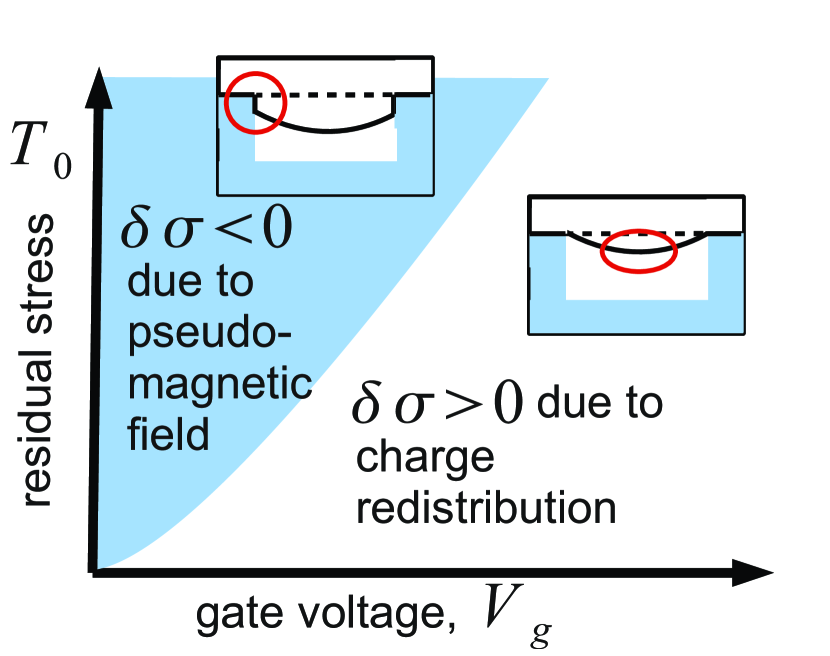
In experiments, graphene flakes are typically suspended over a back-gate. This gate redistributes the electron density in the flake due to the spatial variation of the capacitance. The regions in the center of the suspended part of the flake have higher electron density then the regions near the clamping edges, as the central part is closer to the gate. This density redistribution affects the transmission coefficients through the entire flake. The corresponding effect on the piezoresistivity in ballistic regime is of the first order in the maximum deformation of the flake in the transverse direction, and it increases the conductivity. This has to be contrasted with the effect of the pseudomagnetic fields which suppress the conductivity. The contribution from pseudovector potential depends on the strain Katsnelson over the flake and is of the second order in the maximum deformation. Thus, this contribution is expected to be weaker than effect from the charge redistribution. We will show however that this effect can be important for graphene under high enough residual stress. Inhomogeneous deformation of graphene yields the corrections to the conductivity which are of the fourth order in the maximum deformation, which is even smaller.
In this Article, we calculate the effect of the gate-induced density redistribution on the conductivity of the graphene flake. We find that, indeed, for high residual stress the correction resulting from the pseudovector potential is important, and the correction to the conductivity is negative. We mostly focus on the regime of low residual stress and show that the correction from the charge redistribution becomes the most important.
Experimentally, influence of deformation on the conductivity would be difficult to observe on a suspended graphene flake with one gate since the main effect of the gate is the global shift of the density rather than its redistribution. To separate density redistribution and elastic deformation, one needs to employ two gates. For instance, one can use the configuration with a large bottom gate and a narrow top gate. The bottom gate deforms the graphene flake and determines the maximum transverse deformation . When voltage is switched on the narrow top gate it does not influence much of deformation of the flake depleting the charge density below the top gate. Since the region under the top gate has the lowest density it determines the conductivity of the whole flake. If this region is brought to the Dirac point, the correction to conductivity is determined only by the deformation of graphene Katsnelson and is proportional to , with and being the voltage applied to the bottom gate and the length of the strip under the top gate. However, for higher voltages the charge redistribution is more important, and the correction to conductivity is proportional to , being the distance to the bottom gate. Instead of the top gate, one can use an AFM tip.
The paper is organized as follows. In Section II we derive equations for the deformation of suspended graphene from general theory of elasticity. We consider two situations — graphene deformed homogeneously by a gate and graphene deformed locally by an AFM tip. The capacitance between the gate and suspended graphene varies due to deformation of the flake. We calculate the density redistribution over the flake taking into account the shape of the flake. In Section III, we use these results to evaluate correction to the conductivity. We use the perturbation theory to calculate the transmission eigenvalues, and the correction to the conductivity is obtained using the Landauer formula. This correction can be big for sufficiently strong deformations of the flake which can be produced by an AFM tip. In Section IV we discuss the results and the regimes not considered in this Article.
II Deformation of the graphene sheet
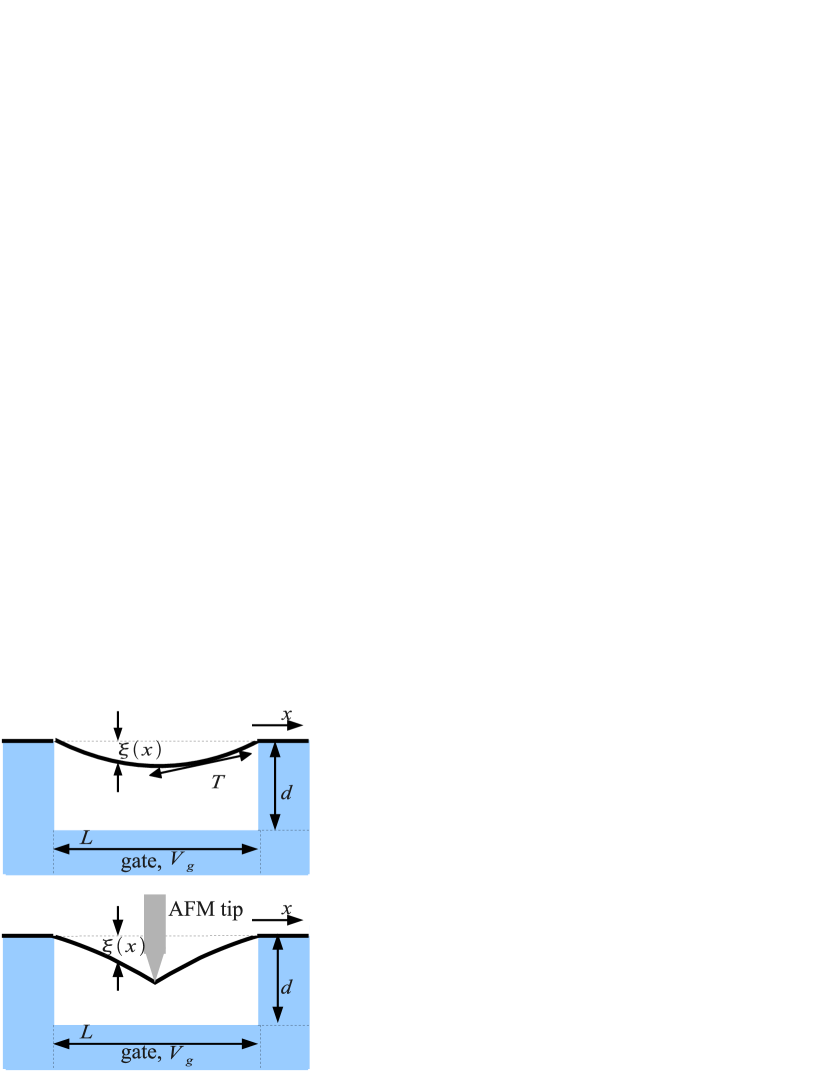
In this Section, we calculate the profile of the graphene sheet formed by electrostatic forces induced by the gates. For this purpose, we decompose the total energy of the flake as the sum of electrostatic and elastic energies. We consider a graphene flake of the length (direction ) and the width (direction ). For simplicity, we assume . An undeformed sheet occupies a part of the plain ; the electrostatically induced deflection is . Below we only consider small deformations so that we can stay within the limits of linear theory of elasticity (Hooke’s law). At stronger deformations, as expected from the general theory Landau and also confirmed by theoretical modeling Isacsson and by experiments Bunch on graphene, non-linear terms become important. However, there is a considerable parameter range, with the displacements up to 50 nm, where the linear regime is still valid. We discuss the terms which go beyond Hooke’s law Isacsson in Section IV.
For electrostatic energy, similarly to Ref. Blanter, , we model the system as a capacitor between the flake and the gate, with the distributed capacitance dependent on the profile of the flake,
| (1) |
Electrostatic coupling to the leads is modelled via contact capacitances , and resistances , , see. Fig (1). The total electrostatic energy of the system carrying the charge is
| (2) |
with .
From now on, we assume that the contacts are ideal, , and thus the electrostatic energy is
| (3) |
The effect of non-ideal contacts is discussed in Section IV.
II.1 Elastic energy
We evaluate the elastic energy in the thin-plate approximation. The elastic energy consists of the bending contribution and the stretching contribution , where is the deformation tensor, and and denote the coordinates in the plane of the sheet ( and ). In the linear regime, the bending contribution is less important than the stretching one, however, we consider both contributions for completeness. Explicitly, we have Landau
| (4) |
and
| (5) |
Here is the bending ridgity, is the Young modulus, is the Poisson ratio, is the thickness of the plate (graphene flake) , and is the stress tensor.
In addition, if a local force (for instance, an AFM tip) acts on the graphene flake, it is best represented by external pressure . The work of this external pressure to deform the flake by is , where is the surface element.
The profile of the sheet is determined by minimizing its total energy. Performing the variation, we find the equation describing the shape of the flake,
| (6) | |||
| (7) |
with being the electrostatic pressure on the plate, induced by the variation of electrostatic energy (3). For ideal contacts, . Here is the electron density. Eq. (6) is the most general equation for in the linear approximation of theory elasticity. For an infinitely wide graphene flake, , the deformation in the direction is homogeneous.
At sufficiently small deformations, the tension along the sheet is constant over the sheet (7), . The tension is the sum of two contributions:
| (8) |
The first one, , is the residual stress which results from the fabrication process or is induced by the ripple formation Delftexp ; Changgu . The second contribution, , is an internal force due to the relative elongation (Hooke’s law). If we take this term into account, we can go beyond the thin-plate approximation and consider deformations bigger then the thickness of the graphene layer.
In the two following Subsections, we solve the above equations for two specific situations: homogeneous external force (which can be produced by a bulk bottom gate), and local force (produced for example by an AFM tip).
II.2 Homogeneous force: Deformation by a bottom gate
Applying a voltage on a bottom gate is a standard way to vary electron density in graphene. If the suspended graphene flake is charged, it is subject to a mechanical force proportional to the charge density. If the area of the gate is much larger than the area of the flake, the electron density induced by the gate is constant almost everywhere, , except for the clamping points of the flake, where it is determined not only by the solution of the Poisson equation (providing singularities at the capacitor edges), but also by the metallic leads to which the flake is clamped. Indeed, experimental evidence for this charge inhomogeneity exist and can be accessed by asymmetry of the Dirac peak in conductivity smth . However, these density inhomogeneities at the clamping areas very little affect the deformation, since the displacement vanishes at the edges of the flake. Therefore we can approximate the effect of the gate by homogeneous electrostatic pressure over the flake, , and being the gate voltage and the distance to the gate. The profile of the graphene sheet is found from the equation
| (9) |
where the stress is constant over the sheet (8) and the deformation-dependent contribution to it depending has to be found self-consistently,
| (10) |
(the case for inhomogeneous derived in Ref. Isacsson, is discussed in Section IV and does not induce significant difference in results). For the boundary condition corresponding to the clamping the sheet, , the profile is
| (11) | |||||
The profile (11) is parabolic in the middle of the strip (as noted in Ref. Katsnelson, ). As we show below, in graphene the dimensionless parameter assumes large values. In this case, the profile can be simplified, and near the middle of the strip has the form
| (12) |
Close to the edges, the profile becomes . Substituting this shape into Eqs. (4) and (5), we find the values of the parameters and ,
| (13) |
and
| (14) |
The maximum vertical displacement obeys the equation
| (15) |
The deformation of the sheet leads to the redistribution of the electron density, which in the Thomas-Fermi approximation is . In its turn, the density redistribution affects the profile of the sheet, and needs, in principle, to be calculated self-consistently. However, as soon as the displacement is much smaller than the distance to the gate, the later effect is insignificant (of the order of ), and we will use the shape (11) not modified by the density redistribution.
The charge over the graphene flake is determined from minimization of the total energy of the system with respect to electron density ,
| (16) |
where the maximum deformation of the sheet in the middle, (15), and depends on charge density. The second term in the brackets and from the third term come from electrostatic energy and originate from the redistribution of the charge density due to variation of the distance between parts of deformed graphene and the gate. The rest () of the third term comes from bending energy. The fourth term takes into account dependence of the stretching force over the flake on the charge density via the deflection (Eq. (10)). Calculations are made under the assumption , which is realistic for available experiments. Simplifying Eq. (16), we obtain
| (17) |
At low gate voltages, Eq. (17) yields the linear gate voltage dependence of the electron density, . There is non-linear deviation from this dependence at higher gate voltages and at rather low initial strain .
The maximum deformation can be expressed analytically in two limiting cases. First, if the residual stress is stronger than the induced stress , it mostly accounts for the deformation of the sheet,
| (18) | |||||
| (19) |
In the case of low residual stress, one obtains
| (20) | |||||
| (21) |
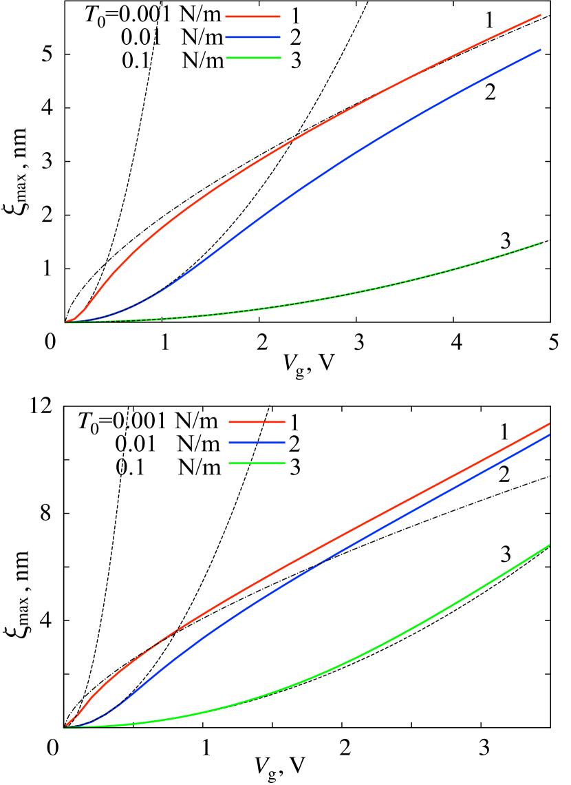
The maximum deviation , obtained from the numerical solution of coupled nonlinear equations Eqs. (15), (17), as well as asymptotic expressions (18) and (20), are shown in Fig. 2 for different values of initial stress foot1 . According to Eqs. (19) and (21), the nonlinear part of the charge induced on the graphene flake follows the dependence .
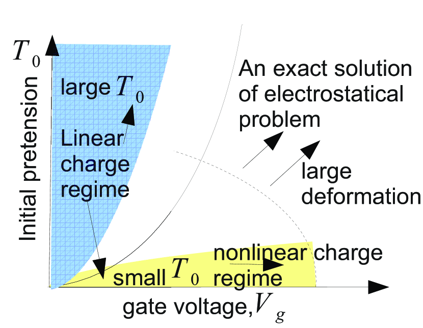
Consequently, we encounter several regimes for the deformation,
- •
-
•
at small and low gate voltages the charge–voltage dependence can be in linear regime, and the maximum deformation follows Eq. (20). We illustrate this for the flake with the parameters N/m and distance to the gate nm (See. Fig. 2, top), where the solutions of coupled electrostatic and elastic equations, Eq. (15), (17), follow asymptotic expression Eq. (20). The charge redistribution does not need to be taken into account;
-
•
at small and large the system is in the non-linear charge regime. This situation can be realized for small distances to the gate when the coupling of the graphene sheet to the gate is large, so that it is possible to create large deformations using low gate voltages. For example, at nm the non-linear charge regime influences the deformation already at voltage V, at the bottom plot Fig. 2 we can see the intersection of the asymptotical curve (20) and the actual solution of Eqs. (15), (17).
The schematic representation of these regimes is shown in Fig. 3.
II.3 Local force: Deformation by an AFM tip
Next, we consider a concentrated force acting on graphene. This force can be provided, for example, by an AFM tip. The effect of the tip is modeled by strong pressure exerted on a narrow area of the width . We assume that the problem is still homogeneous in the -direction, what simplifies the calculations enormously. Inclusion of a pressure action in a narrow circle, which is experimentally relevant for an AFM tip, is not expected to bring qualitatively new features. We consider pressure and . Here is the local pressure, and can describe homogenious pressure due to electrostatics.
The maximum displacement of the flake (realized at the central point) is easy to write down for and :
| (22) | |||||
For and we obtain
| (23) |
The profile of the graphene sheet in this approximation becomes
| (24) |
In the limits of weak and strong residual stress the deformation is determined by
| (25) |
and
| (26) |
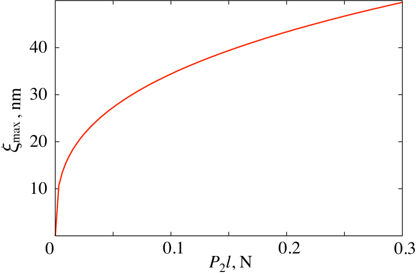
The dependence of the maximum deformation on the applied external local force is shown in Fig. 4. The deformation produced by this force is much bigger than the deformation caused by electrostatic pressure of the gate. The electrostatic problem for this case can be solved separately from the problem of elasticity.
III Piezoconductivity of graphene flake
It was shown experimentally Bolotin2 that suspended graphene flakes are described with good precision as purely ballistic. Theoretically, conductance is determined by Landauer formula Carlo
| (27) |
where is the transmission eigenvalue in the transport channel , and the factor is conductivity of a single transport channel which takes into account valley and spin degeracy. The number of open transport channels is proportional to the Fermi momentum , and thus the conductivity is proportional to the square root of the electron density , .
The conductivity of graphene flake suspended over a gate can deviate from this dependence. To start with, due to electrostatic interaction with the gate, the density becomes inhomogeneous Silvestrov . In particular, Poisson equation leads to the square root divergence of the electron density at the clamping points, as in any capacitor (see e.g. Ref. Morse, ). To treat this divergence properly, one has to take into account electrostatic interaction with the contacts near the edge of the graphene strip, which modifies significantly the electron density near the edge, removing the divergence. However, the effect of this inhomogeneous density close to the contacts does not affect the piezoconductivity of the flake, since the deformation close to the clamping points is very weak, and thus it can be included into the contact resistance at the clamping points.
We now turn to the effects of the deformation on the conductivity. Deformation of graphene can change the conductivity by inducing changes in the band structure (which results in pseudo-magnetic fields) as well as by changing the electron density over the flake. We consider both these mechanisms and will show that typically the effect of the density redistribution dominates.
Electrons in graphene obey Dirac equation. Deformation of the flake influences on the Dirac equation in three ways — it shifts the K-points by a certain amount (pseudomagnetic field), renormalizes the Fermi velocity by , and induces the variation of the electron density on the flake . The deformation correction to the conductivity is thus a function of these three dimensionless parameters.
The pseudomagnetic field, produced by the shift of the -point, is caused by stretching and bending. The shift of the -point due to stretching generates the vector potential Ando ; Katsnelson
| (28) |
where is the order of 1, and , and being the overlap integral in the tight-binding model and the lattice parameter, respectively. For one has , and hence . The deformation is homogeneous within the limits of applicability of Hooke’s law, and thus and . This means that there is no pseudomagnetic field over the graphene flake. The pseudomagnetic field only appears in the region where the flake goes from the substrate to the suspended state Katsnelson and, as noted above, its effect to the piezoconductivity is small, of the second order in ,
| (29) |
where the deformation on the edges has been estimated as , and . Taking into account the value of Cbeta , we obtain
| (30) |
Note the contribution from two terms induced by deformation stress and residual stress, as well as multiplication with the big prefactor .
The underlying physical picture for the model of Ref. Katsnelson, is that the graphene flake is ”glued” to the walls at the suspension point. Whereas this has been realized in some experiments Changgu , it describes the situation when the residual strain is of the same order or higher than the strain induced by the gate voltage. The residual strain results from the fabrication process and is most likely to be created by impurities in the substrate. It can be made low on purpose since the strain is reduced after annealing Chen . In the opposite situation, when the residual stress is not significant, the pseudomagnetic field is inhomogeneous and distributed over the whole suspension area.
The pseudomagnetic field is also inhomogeneous if one considers the bending contribution. Bending leads to the inhomogeneous modification of the overlap of the orbitals, and the resulting pseudovector potential has the form Katsnelson2
| (31) |
being the angle between normal vectors to the graphene surface at the points and , and the constant Kim tbend . The shape dependence of has the form
This yields . Hence the contribution from bending is approximately times smaller then from stretching without residual stress, and is thus negligibly small, even though the resulting magnetic field is not homogeneous.
The easiest way to estimate inhomogeneous stretching of graphene is to take Hooke’s law in the local form, . Since the maximum relative deformation can be estimated as , naively, the correction from non-homogeneous stretching is of the same order as the one from delta-functional pseudomagnetic field at the clamping edges. We show below, however, that the correction from non-uniform stretching is of the order of , but still due to large prefactor it can reduce the conductivity at low gate voltages.
Another effect induced by the deformation is the renormalization of the Fermi velocity. The renormalized value of the velocity can be derived from the tight-binding model. Assuming that the graphene sheet is only deformed in the -direction, we find that the -component of the Fermi velocity is unchanged wheres the -component is renormalized,
| (32) |
so that approximately . The effect of the renormalization on the conductivity is not significant and has the order of magnitude . Note that this is the same dependence on as for pseudomagnetic fields, however, it is not enhanced by a big prefactor.
The influence on conductivity of such change in fermi-velocity is not significant. This influence can be in principe measured experimentally as the conductivity variation at the Dirac point, similarly to how we explain below in Subsection III.2.
III.1 Correction to conductivity due to the charge redistribution
Redistribution of electric charge due to interactions with the gate is found from the assumption that the potential along the graphene sheet is constant, , where is the capacitance of the element of the length of graphene, , and is the charge of this element. In the first order approximation, this gives .
The conductivity of graphene is proportional to charge density , and thus the contribution to conductivity due to charge redistribution is expected to be linear in the maximum deviation from the homogeneous density, . Thus, the correction to conductivity is expected to be .
Before starting the calculation of the correction to conductivity, we estimate the range where this correction of the order of is more important than the correction due to pseudovector potential which we considered above, Fig. 5,
| (33) |
As noticed in Ref. Katsnelson, the pseudovector potential at low gate voltages blocks conductivity, this is seen from Eq. (30). For large deformation the expressions (20) are valid, residual stress is not important any more, and thus the gate voltage should be large enough to see the decrease of conductivity,
| (34) |
This deformation is so strong that in can not be reached in practice.
For the deformation with AFM the residual stress is not important and at deviations
| (35) |
correction to pseudovector potential starts to suppress the conductivity.
To calculate the correction due to the charge redistribution, we notice that the density variation is translated into the correction for conductivity via the variation of the transmission probabilities , which are the eigenvalues of the matrix , being the transmission matrix of the graphene sheet. The transmission eigenvalues are determined in Appendix by the transfer matrix method. The correction to the conductivity is linear in the density shift , and consequently in the maximum deformation (as is shown above from simple qualitave considerations). It has the form (see Appendix)
| (36) | |||||
where is the transmission probability for the mode labeled by the transverse momentum , being an integer number, and is a wave number in the direction along the strip, so that .
To carry out more detailed analysis, we consider specific deformation setups discussed in Section II — homogeneous and local deformation.
Eq. (36) can be analyzed analytically for small and large values of the parameter , which characterizes the charge density over the flake. The correction to conductivity for the homogeneous deformation (bottom gate) has the following asymptotic behavior for small and large values of (for more details, see Appendix),
| (37) |
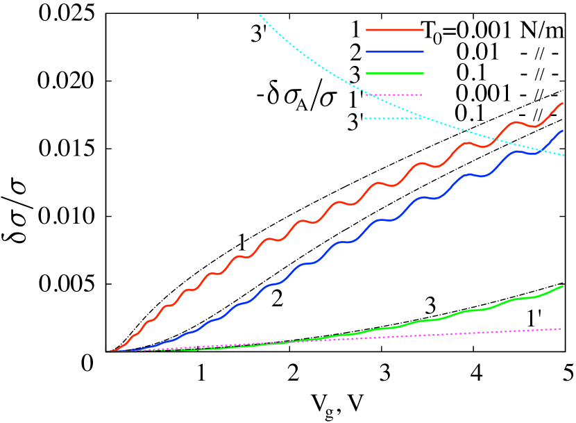
Taking into account the functional dependence of the maximum deviation for small and large initial stress , Eqs. (20) and (18), we get the asymptotic dependence of the correction to conductivity on the gate voltage, for :
| (38) |
and for :
| (39) |
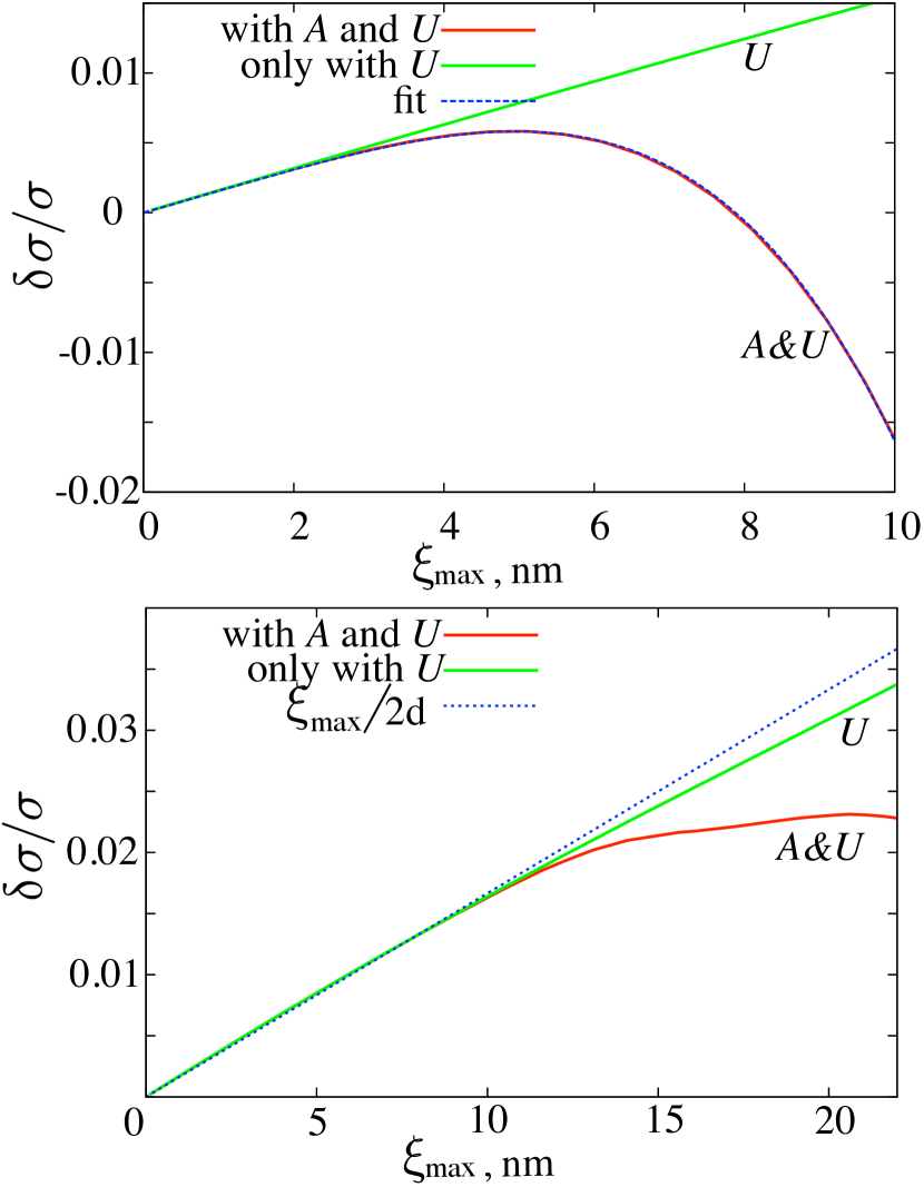
Fig. 6 shows the exact result of summation over modes Eq. (36). At both high () and low () gate voltages, the correction follows the asymptotic behavior both for weak and strong residual stress , Eqs. (39) and (38). On the same plot we compare the correction we found with the correction due to pseudomagnetic fields at the edges Katsnelson . The latter one has a different sign (conductivity decreases with the stress). For high residual stress this correction is more important than due to charge redistribution, according to Ref. Katsnelson, it can block conductivity. For low residual stress it is about 10 times lower than the increasing conductivity correction. The oscillations of have the period of d are associated with the shift of Fabry-Perot resonances in conductivity for deformed graphene flake as conpared with an undeformed flake. This shift occurs since the effective longitudinal wave vector of an electron in graphene depends on the deformation since it feels different charge density over the graphene flake. Note also that the contribution from pseudomagnetic fields does not oscillate since the value of is the same for the whole flake. The first order perturbation theory in is valid until this parameter reaches a rather large value, (see Appendix for more details).
For the case of local deformation, using the graphene profile (24) and using the same technique as in Appendix, we find the correction for conductivity due to the charge redistribution,
| (40) |
Note that the asymptotic behavior for large has the same form as for homogeneous deformation.
We can also estimate the influence of inhomogeneous pseudomagnetic field assuming the local form of Hooke’s law as in Isacsson and using the perturbation theory for the transfer matrix, as detailed in Appendix. We find that the first order perturbation theory correction in pseudovector potential vanishes, whereas the second order correction can be estimated as
| (41) |
At low gate voltages and large deformations (for instance, induced by local deformation), this correction can be more important that the one from the charge redistribution, and thus the conductivity will be suppressed. From comparison of Eqs. (41) and (40) this supression happens for deformations:
| (42) |
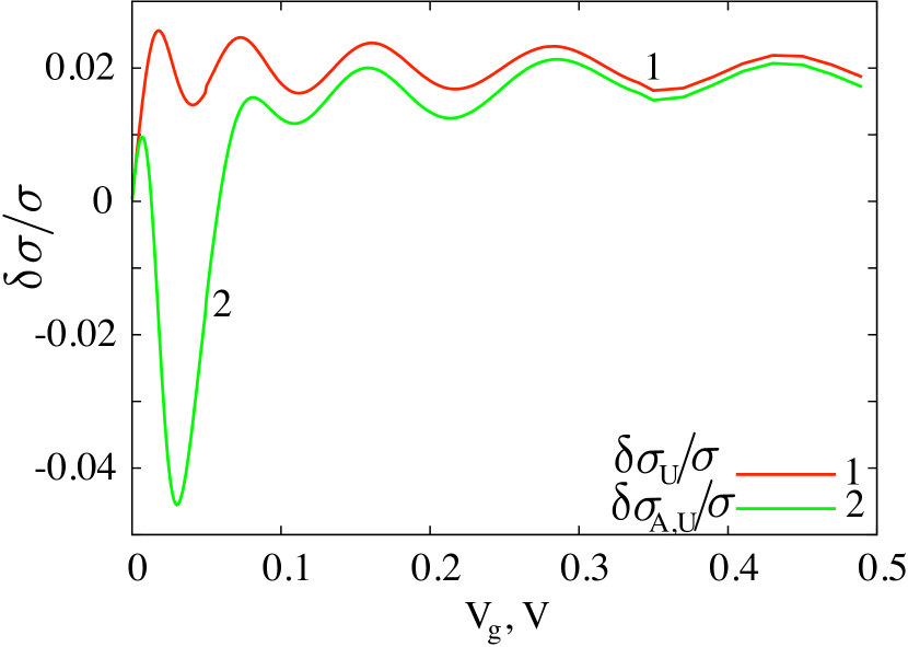
We demonstrate this by solving numerically by transfer matrix method the Dirac equation with additional potential due to charge redistribution and pseudovector potential, Fig. 7. At fixed large nm (estimated using Eq. (42)) and at low voltages the conductivity starts to decrease due to inhomogeneous tension distribution in the flake, and at higher voltages increases again due to the effect of charge redistribution. Fig. 8 shows that for small gate voltages lower maximum deformation is required to reach the point where the conductivity starts to decrease, in agreement with Eq. (41). For high gate voltages V pseudomagnetic fields lead to saturation of the conductivity rather than to its decrease.
III.2 Two-gate geometry
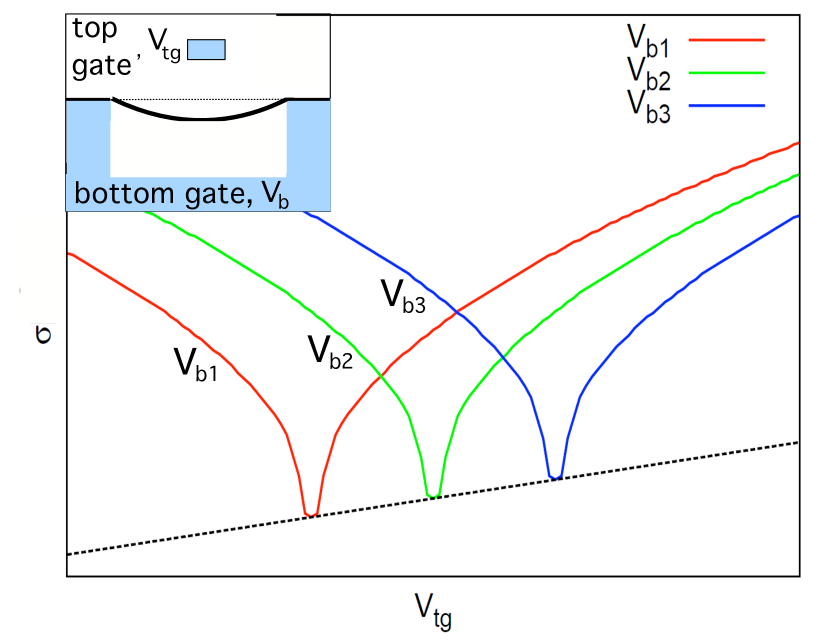
Conductivity can also be used to measure relative stretching of deformed suspended graphene. Note that the influence of stretching on the conductivity of graphene deposited on a substrate has been demonstrated experimentally grow3 . For suspended graphene it is more difficult to extract the value of stretching than from the graphene on the substrate, since the gate voltage simultaneously varies the concentration and deforms graphene, as shown above.
To measure relative stretching of suspended graphene, we propose the two-gate geometry (Fig. 9). The deformation of the graphene flake is created by the large bottom gate, the influence of the top gate on the deformation is small as the top gate is narrow. The top gate is used to vary the charge density in the region underneath it. In this geometry at the fixed voltage at the bottom gate one can move through the Dirac point by varying the voltage at the top gate (the experiment for bilayer with two gates on the substrate Oostinga ). The value of conductivity at this point depends on the deformation.
The stretching of the graphene flake, as discussed above, induces variations of the conductivity for two reasons. First, it induces pseudomagnetic fields. These, however, can be gauged away of Dirac equation Ludwig at the Dirac point and do not influence the conductivity. Second, it shifts the Fermi velocity. The relative shift is proportional to the deformation, , and leads to the positive correction of the conductivity at the Dirac point, . Thus, for different bottom gate voltages, which is equivalent to different maximum deformations , the conductivity at the Dirac point is slightly different, and the relative graphene stretching can be restored from this dependence. For example, consider the dependence of conductivity on the top gate voltage for different bottom gate voltages (Fig. 9). At a fixed value of the bottom gate voltage, the conductivity as a function of the top gate voltage exhibits a peak dependence, with the minimum corresponding to the Dirac point. The difference between the values of conductivity at Dirac peaks, , for different bottom gate voltages, and , is proportional to the difference in relative deformation, (we remember that ).
IV Discussion
In this Article, we investigated two mechanisms which affect the conductivity of suspended graphene — charge redistribution induced by the gate(s), and pseudomagnetic fields induced by the deformation of graphene. We find that for the small residual stress , the charge redistribution mechanism dominates. For low gate voltages and strong deformation, which experimentally is best realized by using AFM, the correction due to nonuniform pseudomagnetic fields is more significant. The correction due to pseudovector potential at the region of suspension can decrease conductivity at the large residual stress Katsnelson . It is important that the two mechanisms provide corrections to conductivity which are of different signs. Indeed, the correction from pseudomagnetic fields suppresses the conductivity Katsnelson by shifting K-points due to the vector potential. The shift is different at different points of the suspended sample, and if the deformation is big enough, the Fermi circles at the clamping points and at the centre of the flake do not overlap: The system becomes insulating. If now we take into account the effects of the gate, not only the Fermi circles are shifted, but their radii are greater at the center of the flake since the charge density is greater in the areas closer to the gate. The increase of the radii and the shift of the center compete, and we find that typically the radius increase is more important.
It is difficult to measure piezoconductivity only by using a bottom gate since the gate voltage not only bends graphene and produces the correction to the conductivity, but also shifts the overall charge density. The density dependence of the conductivity is different from the density dependence of the correction. Thus, to extract the value of piezoconductivity, one has to compare the conductance of deformed and undeformed graphene sheet at the same density, which can only be done in the one-gate geometry by comparing the results with the theoretical prediction. In contrast, the two-gate setup, with a bottom gate fixing the overall density and the top gate (which can be an AFM tip) creating the deformation is more convenient to extract piezoconductivity. One can fix the voltage on the bottom gate and start to deform the flake with the AFM tip. At low gate voltages the conductivity decreases due to the pseudomagnetic fields, whereas at higher voltages it starts to grow due to the charge redistribution.
In the real experimental situation, the AFM tip has a point shape, whereas in this Article we considered for illustration the deformation homogeneous in one direction, i.e. replaced the tip by a rod. Non-homogeneous deformation in all directions creates pseudomagnetic fields, with the conductivity depending not only on the transverse displacement, but also locally on the position over the graphene sheet. The conductivity is the largest if the tip is placed in the middle of the sheet, and decreases if the tip moves to the side. We can understand this behavior from a simple reasoning. Indeed, the electrons which from the two sides of the tip feel the pseudomagnetic fields and interfere similarly to an Aharonov-Bohm ring. The interference is more destructive if the tip is further from the center, and thus the conductivity decreases.
Another parameter which affects the conductivity is the residual stress . It can be varied experimentally for instance if one uses graphene suspended over piezosubstrate. Putting voltage on the substrate would induce extra stress on graphene, and one can move from the situation where pseudovector potential blocks the conductivity at low gate voltages to the case where residual stress does not play a role and the correction due to charge redistribution increases the conducitivity.
In this Article, we considered ideal ballistic graphene. In particular, we disregarded the contact resistance, assuming the clamping points to be ideal contacts. Finite transparency of the contacts would suppress both the conductivity itself and the piezocorrection to the conductivity; in addition, it would raise the amplitude of Fabry-Perot resonances.
For strong deformations of the graphene sheet, the problem becomes much more complicated, since one has now to solve elasticity equations self-consistently, taking into account that the displacement depends on the charge redistribution. This leads to additional terms in the equations of the elasticity theory. Taking into account influence of the density redistribution on the term with electrostatic pressure in the equation of deformation, one can show that the self-consistency condition increases the deformation in the middle of the graphene sheet. This effect only becomes important at sufficiently strong deformations.
Finally, we assumed that undeformed graphene is flat. In reality, it is always rippled, and, in principle, one needs to use the elasticity theory for membranes. However, we do not expect that taking ripples into account would significantly affect the results of this paper. First, the ripples are small and have a large radius of curvature, which means they are very little affected by the overall deformation of the graphene sheet. Second, the main effect of the ripples is to renormalize the energy over the graphene sheet Ostrovsky . We thus expect that our results are valid, but for renormalized energy over the flake (energy is determined by gate voltage in clean case, and is renormalized in the rippled case).
V Acknowledgements
We thank A. Akhmerov, C. Beenakker, M. Fogler, S. Goossens, F. Guinea, A. Isacsson, and A. Kharimkhodjaev for discussions. We acknowledge the financial support of the Future and Emerging Technologies program of the European Commission, under the FET-Open project QNEMS (233992), of the Dutch Science Foundation NWO/FOM and of the Eurocores program EuroGraphene.
VI Appendix. Perturbative corrections to conductivity
In this Appendix, we calculate the corrections to the conductivity due to both charge redistribution and pseudomagnetic fields, using the preturbation theory.
The Dirac equation for one valley in graphene has the form
| (43) |
with , ,
and being the components of the pseudomagnetic vector-potential Cbeta , given by Eq. (28), and is the additional electrostatic potential due to the charge redistribution over the graphene flake. It is determined by local variations of the Fermi energy over the flake. Since the Fermi energy depends on the charge density over the flake, , , one has
We only consider the deformation homogeneous in -direction.Then both and only depend on the coordinate , and (see Section III). The problem becomes effectively one-dimensional since the momentum in -direction is conserved. It is convenient to use the transfer matrix representation of Dirac equation Ostrovsky to calculate the correction to the conductivity caused by the deformation , ,
where is the Hadamard transformed transfer matrix, and is the Hadamard transformed transfer matrix of the unperturbed system,
| (45) |
We perform the perturbation expansion of the integral form for Eq. (VI), and in the first order in and we obtain
| (46) | |||
The conductance of the graphene sheet is determined by Landauer formula (27). According to general scattering theory Ostrovsky , the transmission matrix element is an inverse element of ,
| (47) |
Taking into account Eq. (VI), Landauer formula (27), and the definition (47), the first order corrections to conductivity due to electrostatics and pseudo-magnetic field are
| (48) | |||||
| (49) |
| (50) | |||||
where is a wave vector in the -direction, is an integer number, and is a wave vector along the strip,
Furthermore, is the transmission probability for clean system for the mode , and
Note that the first-order correction due to the pseudo-vector potential (49) only contains odd powers of , so that the sum over vanishes. Thus, the first-order correction to the conductivity is determined solely by the density redistribution. It is linear in the maximum deviation for small deviations.
First, we remark on the validity of Eq. (48). The expansion of the expression
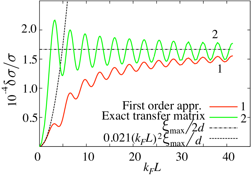
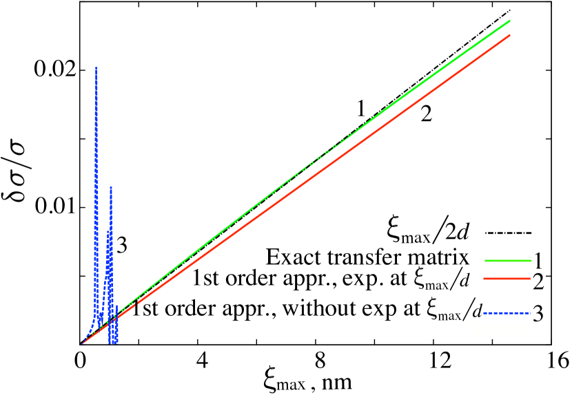
has been made under assumption that the second term is small in comparison with unity due to the small prefactor . Following this argument, the expression for the first order correction to the conductivity in is formally only valid for . However, solving the integral equation numerically, we find that this expression is valid for a broader parameter range. We compare results of calculations for the first order correction Eq. (48) and numerical solution of Eq. (VI) for the two cases: for the fixed ratio and for the fixed value of . For the first case, the dependence of on shows the same oscillation period and the same asymptotic behavior at large , Fig. 10. For the second case, at large (for the distance to the gate nm this corresponds to the gate voltage V) the expansion clearly ceases to be valid, see Fig. 11. We thus conclude from the results of our numerical solution that the expression for the correction linear in is applicable until , which is weaker than the perturbation theory suggestion .
The second order correction to conductivity contains also a term with the pseudo-vector potential, the magnitude of the term being .
We consider both corrections separately. Now we perform the analysis of Eq. (48) for deformation with constant pressure. For this case, the shape of the strip is nearly parabolic (Section II) and can be approximated as
The integral with the induced potential from Eq. (48), , is
| (51) |
Now we can perform the summation over modes for , Eq. (48), analytically in two asymptotic cases: and .
For , the evanescent modes give the most important contribution to the conductivity BeenakkerR ,
| (52) |
and to the correction to the conductivity,
| (53) |
with
and its numerical value is . The relative correction to conductivity reads
| (54) |
For we average over fast oscillations. In this case, only the propagating modes contribute significantly to the conductivity.
To perform the averaging, we replace the summation over by the integration,
To simplify subsequent calculations, we make the change of variables , , and then go from the integral over to the integral over . The correction to the conductivity Eq. (48) has the form
In this expression only the term with from Eq.(51) survived: All terms with vanish after averaging, and the term with is smaller than one which is taken into account). For large the terms and in Eq. (48) oscillate very rapidly. We can represent as a sum of fast oscillating terms, with each term being an average over the period,
with . The integrand is determined by structure of Eq. (48) and Eq. (51),
What is left is the sum over ,
| (55) |
. Finally,
| (56) |
The conductivity after averaging over fast oscillations becomes , and the relative correction to the conductivity is
From general physical considerations about the correction (see main text), one also expects the dependence for .
Concerning the correction due to the pseudomagnetic fields, it is of the second order in , and the analytical expressions are too cumbersome. Instead, we illustrate our conclusions using the numerical solution of the integral equation (VI). It is done by multiplying transfer matrices for small intervals of the length . Convergence with the size of is reached.
References
- (1) C. W. J. Beenakker, Rev. Mod. Phys. 80, 1337 (2008)
- (2) A. H. Castro Neto, F. Guinea, N. M. R. Peres, K. S. Novoselov, and A. K. Geim Rev. Mod. Phys. 81, 109 (2009).
- (3) C. Lee, X. Wei, J. W. Kysar, and J. Hone, Science 321, 385 (2008).
- (4) M. Poot and H. S. J. van der Zant, Appl. Phys. Lett. 92, 063111 (2008)
- (5) I. W. Frank, D. M. Tanenbaum, A. M. Van der Zande, and P. L. McEuen, J. Vac. Sci. Technol. B 25, 2558 (2007)
- (6) Q. Lu, M. Arroyo, and R. Huang, J. Phys. D 42, 102002 (2009).
- (7) J. Zhou and R. Huang, J. Mech. Phys. Solids 56, 1609 (2008).
- (8) J. S. Bunch, A. M. van der Zande, S. S. Verbridge, I. W. Frank, D. M. Tanenbaum, J. M. Parpia, H. G. Craighead, and P. L. McEuen, Science 315, 490 (2007).
- (9) C. Chen, S. Rosenblatt, K. I. Bolotin, W. Kalb, P. Kim, I. Kymissis, H. L. Stormer, T. F. Heinz, and J. Hone, Nature Nanotechnology 4, 861 (2009).
- (10) Keun S. Kim, Y. Zhao, H. Jang, S. Y. Lee, J. M. Kim, Kwang S. Kim, J.-H. Ahn, P. Kim, J.-Y. Choi, and B. H. Hong, Nature 457, 706 (2009).
- (11) T. M. G. Mohiuddin, A. Lombardo, R. R. Nair, A. Bonetti, G. Savini, R. Jalil, N. Bonini, D.M. Basko, C. Galiotis, N. Marzari, K. S. Novoselov, A. K. Geim, A. C. Ferrari, Phys. Rev. B, 79, 205433 (2009).
- (12) K. I. Bolotin, K. J. Sikes, Z. Jiang, M. Klima, G. Fudenberg, J. Hone, P. Kim, and H. L. Stormer, Solid State Commun. 146, 351 (2008).
- (13) K. I. Bolotin, K. J. Sikes, J. Hone, P. Kim, and H. L. Stormer, Phys. Rev. Lett. 101, 096802 (2008).
- (14) J. Velasco Jr., G. Liu, W. Bao, and C. N. Lau, New J. Phys. 11, 095008 (2009).
- (15) X. Du, I. Skachko, F. Duerr, A. Luican, and E. Y. Andrei, Nature, 462, 192 (2009).
- (16) V. M. Pereira and A. H. Castro Neto, Phys. Rev. Lett. 103, 046801 (2009).
- (17) M. M. Fogler, F. Guinea, and M. I. Katsnelson, Phys. Rev. Lett. 101, 226804 (2008).
- (18) R. M. Ribeiro, Vitor M. Pereira, N. M. R. Peres, P. R. Briddon, and A. H. Castro Neto, New J. Phys. 11, 115002 (2009).
- (19) H. Suzuura and T. Ando, Phys. Rev. B 65, 235412 (2002).
- (20) T. Stauber, N. M. R. Peres, and A. H. Castro Neto, Phys. Rev. B 78, 085418 (2008).
- (21) K.-Y. Kim, Ya. M. Blanter, and K.-H. Ahn (unpublished).
- (22) Y. Hernandez, V. Nicolosi, M. Lotya, F. M. Blighe, Z. Sun, S. De, I. T. McGovern, B. Holland, M. Byrne, Y. K. Gun’Ko, J. J. Boland, P. Niraj, G. Duesberg, S. Krishnamurthy, R. Goodhue, J. Hutchison, V. Scardaci, A. C. Ferrari, and J. N. Coleman, Nature Nanotechnology 3, 563 (2008).
- (23) L. D. Landau and E. M. Lifshits, Theory of Elasticity (Pergamon, Oxford, 1986).
- (24) J. Atalaya, A. Isacsson and J. M. Kinaret, Nano Lett. 8 (12), 4196, (2008).
- (25) S. Sapmaz, Ya. M. Blanter, L. Gurevich, and H. S. J. van der Zant, Phys. Rev. B 67, 235414 (2003).
- (26) We consider the experimentally feasible parameters of the graphene flake: Length , distance to the gate nm, Young modulus TPa, Poisson ratio , and thickness of the graphene monolayer nm.
- (27) J. Tworzydlo, B. Trauzettel, M. Titov, A. Rycerz, and C. W. J. Beenakker, Phys. Rev. Lett. 96, 246802 (2006).
- (28) P. G. Silvestrov and K. B. Efetov Phys. Rev. B 77, 155436 (2008).
- (29) H. Feshbach and P. Morse, Methods of Theoretical Physics, (University Press, Cambridge, 1953).
- (30) Parameter can be taken in the form , where according to calculations Woods , N/m2, and the parameter , can be determined by different methods, it is approximetely (from femtosecond time-resolved photoemission experiement Hertel , , from analitycal estimations Pietronero and optical spectrum of polyacetylene, , from tight-binding approximation ). Finally, the estimation of the is .
- (31) Y. Huang, J. Wu, and K. C. Hwang, Phys. Rev. B 74, 245413 (2006).
- (32) E. Kim and A. H. Castro Neto, Europhys. Lett. 84, 57007 (2008).
- (33) follows from consideration of orbital overlapping.
- (34) J. B. Oostinga, H. B. Heersche, X. Liu, A. F. Morpurgo and L. M. K. Vandersypen, Nature Materials 7, 151 (2007).
- (35) A. W. W. Ludwig, M. P. A. Fisher, R. Shankar, and G. Grinstein, Phys. Rev. B 50, 7526 (1994).
- (36) A. Schuessler, P. M. Ostrovsky, I. V. Gornyi, and A. D. Mirlin, Phys. Rev. B 79, 075405 (2009).
- (37) L. M. Woods and G. D. Mahan, Phys. Rev. B 61, 10651 (2000).
- (38) T. Hertel and G. Moos, Phys. Rev. Lett. 84, 5002 (2000).
- (39) L. Pietronero, S. Strassler, H. R. Zeller, and M. J. Rice, Phys. Rev. B 22, 904 (1980).
- (40) S. Russo, M. F. Craciun, M. Yamamoto, A. F. Morpurgo, and S. Tarucha, Phys. E 42, 677 (2010); B. E. Feldman, J. Martin, and A. Yacoby, Nature Physics 5, 889 (2009).
- (41) Note that the conductivity in our considerations and in Ref. Katsnelson, are calculated for different models of the leads. We use the model with infinitely doped leads like in Ref. BeenakkerR, , whereas in Katsnelson graphene has the same potential as the leads.