Graphene Photonics and Optoelectronics
Abstract
The richness of optical and electronic properties of graphene attracts enormous interest. Graphene has high mobility and optical transparency, in addition to flexibility, robustness and environmental stability. So far, the main focus has been on fundamental physics and electronic devices. However, we believe its true potential to be in photonics and optoelectronics, where the combination of its unique optical and electronic properties can be fully exploited, even in the absence of a bandgap, and the linear dispersion of the Dirac electrons enables ultra-wide-band tunability. The rise of graphene in photonics and optoelectronics is shown by several recent results, ranging from solar cells and light emitting devices, to touch screens, photodetectors and ultrafast lasers. Here we review the state of the art in this emerging field.
I Introduction
Electrons propagating through the bi-dimensional structure of graphene behave as massless Dirac fermionsGeim_nmat ; Charlier ; Wallace_1947 , having a linear energy-momentum relation. Consequently, graphene exhibits electronic properties for a two dimensional (2d) gas of charged particles described by the relativistic Dirac equation, rather than the non-relativistic Schrödinger equation with an effective massGeim_nmat ; Charlier , with carriers mimicking particles with zero mass and an effective “speed of light”m/s.
Graphene has revealed a variety of transport phenomena characteristic of 2d Dirac fermions, such as specific integer and fractional quantum Hall effectsZhang_Nature2005 ; andrei , a ”minimum” conductivity even when the carrier concentration tends to zeroGeim_nmat , Shubnikov-de Haas oscillations with phase shift due to Berry’s phaseGeim_nmat . Mobilities, , up to are observed in suspended samples. This, combined with near-ballistic transport at room temperature, makes graphene a potential material for nanoelectronicsLemme_IEEE ; Han_PRL , especially for high frequencylin_10 .
Graphene also shows remarkable optical properties. Despite being a single atom thick, it can be optically visualizedCasi_nanolett ; Blake_APL . Its transmittance can be expressed in terms of the fine structure constantNair_Science ; Kravets . The linear dispersion of the Dirac electrons enables broadband applications. Saturable absorption is observed as a consequence of Pauli blockingHasan_AM ; Sun_graphene , non equilibrium carriers result in hot luminescenceNLPL . Chemical and physical treatments also enable photoluminescencegokusacsnano ; edaadvmater ; sunnanores ; luoapl . These properties make it an ideal photonic and optoelectronic material.
II Electronic and optical properties
II.1 Electronic properties
The electronic structure of single layer graphene (SLG) can be described using a tight-binding HamiltonianCharlier ; Wallace_1947 . Since the bonding and anti-bonding bands are well separated in energy (10 eV at ), they can be neglected in semi-empirical calculations, retaining only the two remaining bandsWallace_1947 . The electronic wavefunctions from different atoms on the hexagonal lattice overlap. However, such an overlap between the () and the or and orbitals is strictly zero by symmetry. Consequently, the electrons, which form the bonds, can be treated independently from the other valence electrons. Within this -band approximation:
| (1) |
where (=1.42 Å is the carbon-carbon distance) and is the transfer integral between first neighbor orbitals (typical values for are 2.9-3.1eV). The vectors in the first Brillouin zone (BZ) constitute the ensemble of available electronic momenta.
With one pz electron per atom in the - model (the three other electrons fill the low-lying band), the (-) band (negative energy branch) in Eq. 1 is fully occupied, while the (+) branch is totally empty. These occupied and unoccupied bands touch at the points. The Fermi level is the zero-energy reference, and the Fermi surface is defined by and .
Expanding Eq. 1 at yields the linear and bands for Dirac fermions:
| (2) |
where , and is the electronic group velocity: .
The linear dispersion given by Eq. 2 is the solution to the following effective Hamiltonian at the point:
| (3) |
where , and ’s are the pseudo-spin Pauli matrices operating in the space of the electron amplitude on the A-B sublattices of graphene.
II.2 Linear optical absorption
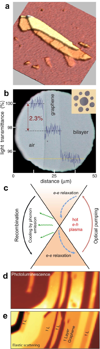
The optical image contrast can be used to identify graphene on top of a Si/SiO2 substrate (Fig.1a). This scales with the number of layers and is the result of interference, with SiO2 acting as a spacer. The contrast can be maximized by adjusting the spacer thickness or the light wavelengthCasi_nanolett ; Blake_APL .
The transmittance (T) of a freestanding SLG can be derived by applying the Fresnel equations in the thin film limit for a material with a fixed universal optical conductanceKuzmenko_2008_PRL , to give:
| (4) |
where is the fine structure constantNair_Science . Graphene only reflects of the incident light in the visible regionNair_Science , raising to 2% for 10 layersCasi_nanolett . Thus, we can take the optical absorption of graphene layers to be proportional to the number of layers, each absorbing A=1-T==2.3% over the visible spectrumNair_Science , Fig.1b. In a few layer graphene (FLG) sample, each sheet can be seen as a bi-dimensional electron gas, with little perturbation from the adjacent layers, making it optically equivalent to a superposition of almost non-interacting SLGCasi_nanolett . The absorption of SLG is quite flat from 300 to 2500nm with a peak in the UV region (250nm), attributed to inter-band electronic transition from the unoccupied statesKravets . In FLG, other absorption features can be seen at lower energies, associated with inter-band transitionsWang_science_2008 ; Mak .
II.3 Saturable absorption
Interband excitation by ultrafast optical pulses produces a non-equilibrium carrier population in the valence and conduction bands, Fig.1c. In time-resolved experimentsBreusing_PRL two relaxation time scales are typically seen. A faster one, , usually associated with carrier-carrier intraband collisions and phonon emission, and a slower one, on a ps scale, corresponding to electron interband relaxation and cooling of hot phononskampfrathprl05 ; lazzeriPRL .
The linear dispersion of the Dirac electrons implies that for any excitation there will always be an electron-hole pair in resonance. A quantitative treatment of the electron-hole dynamics requires the solution of the kinetic equation for the electron and hole distribution functions and , being the momentum counted from the Dirac pointSun_graphene . If the relaxation times are shorter than the pulse duration, during the pulse the electrons reach a stationary state and collisions put electrons and holes in thermal equilibrium at an effective temperatureSun_graphene . The populations determine electron and hole densities, total energy density and a reduction of photon absorption per layer, due to Pauli blocking, by a factor of . Assuming efficient carrier-carrier relaxation (both intraband and interband) and efficient cooling of the graphene phonons, the main bottleneck is energy transfer from electrons to phononsSun_graphene .
For linear dispersions near the Dirac point, pair carrier collisions cannot lead to interband relaxation, thereby conserving the total number of electrons and holes separatelySun_graphene ; Guinea96 . Interband relaxation by phonon emission can occur only if the electron and hole energies are close to the Dirac point (within the phonon energy). Non-equilibrium electron-hole recombination is also possibleNLPL . For graphite flakes the situation is different: the dispersion is quadratic, and pair carrier collisions can lead to interband relaxation. Thus, in principle, decoupled SLG can provide the highest saturable absorption for a given amount of materialSun_graphene .
II.4 Luminescence
Graphene could be made luminescent by inducing a band gap, following two main routes. One is by cutting it into ribbons and quantum dots, the other is by chemical or physical treatments, to reduce the connectivity of the electrons network. Even though graphene nanoribbons (GNRs) have been produced, with varying band gapsHan_PRL , to date no photoluminescence (PL) has been reported from them. However, bulk graphene oxide (GO) dispersions and solids do show a broad PLedaadvmater ; sunnanores ; luoapl ; KPlohACSnano . Individual graphene flakes can be made brightly luminescent by mild oxygen plasma treatmentgokusacsnano . The resulting PL is uniform across large areas, as shown in Figs. 1d,e, where a PL map and the corresponding elastic scattering image are compared. It is possible to make hybrid structures by etching just the top layer, while leaving underlying layers intactgokusacsnano . This combination of photoluminescent and conductive layers could be used in sandwich light-emitting diodes. Luminescent graphene-based materials can now be routinely produced covering the infrared (IR), visible and blue spectral rangegokusacsnano ; edaadvmater ; sunnanores ; luoapl ; KPlohACSnano .
Even though some groups assigned PL in GO to band-gap emission from electron confined islandsedaadvmater ; sunnanores ; luoapl , this is more likely to arise from oxygen related defect statesgokusacsnano . Whatever the origin, fluorescent organic compounds are of significant importance to the development of low-cost opto-electronic devicessheaths . Blue PL from aromatic or olefinic molecules is particularly important for display and lighting applicationsrothberg . Luminescent quantum dots are widely used for bio-labeling and bio-imaging. However, their toxicity and potential environmental hazard limit widespread use and in-vivo applications. Fluorescent bio-compatible carbon-based nanomaterials, may be a more suitable alternative. Fluorescent species in the IR and near-IR are useful for biological applications since cells and tissues exhibit little auto-fluorescence in this regionFrangioni_JV . Ref. sunnanores, exploited PL GO for live cell imaging in the near-infrared with little background.
Ref. Wang_science_2008, reported a gate-controlled, tunable gap up to 250meV in BLG. This may enable novel photonic devices for far IR light generation, amplification and detection.
Broadband non-linear PL is also possible following non equilibrium excitation of untreated graphene layers, Fig 1c, as recently reported by several groupsNLPL . Emission was observed throughout the visible spectrum, for energies both higher and lower than the exciting one, in contrast to conventional PL processesNLPL . This broadband non linear-PL arises from recombination of a distribution of non-equilibrium electrons and holes, generated by rapid scattering between photo-excited carriers after optical excitationNLPL . It scales with the number of layers and can be used as a quantitative imaging tool, as well as to reveal the hot electron-hole plasma dynamicsNLPL , Fig 1c.
Electroluminescence was also recently reported in pristine grapheneEssig . Although the power conversion efficiency is lower than carbon nanotubes (CNTs), this could lead to novel emitting devices based entirely on graphene.
III Production
Graphene was first produced by micromechanical exfoliation of graphiteNovoselov_PNAS . This still gives the best samples in terms of purity, defects, mobility and optoelectronics properties. However, large scale assembly is needed for the widespread application of this material. Several techniques have been developed to provide a steady supply of graphene in large areas and quantities, amenable for mass applications. These comprise growth by chemical vapor depositionKaru_JAP_1966 ; Obraztsov_Carbon ; Kim_nature ; Reina_NL_2009 ; Bae_arxiv , segregation by heat treatment of carbon containing substratesBerger ; Sutter_nmat ; Emtsev_nmat , liquid phase exfoliationLi_Science ; Hernandez_nnano ; Lotya_JACS ; Valles_Jacs ; Stankovich_Nature . In fact, most of these methods date back several decades. The current interest in graphene pushed these early approaches to large yields, controlled growth, large areas, and enabled in just 6 years to go from micrometer flakes to near mass production of layer controlled samples.
III.1 Micromechanical cleavage
Micromechanical cleavage (MC)Novoselov_PNAS consists in peeling off a piece of graphite by means of an adhesive tape. MC has been optimized to give SLG up to mm in size, of high structural and electronic quality. Although this is the method of choice for fundamental research, and most key results on individual SLG were obtained on MC flakes, it has disadvantages in terms of yield and throughput, and is impractical for large scale applications.
III.2 Liquid phase exfoliation
Liquid phase exfoliation (LPE) of graphite consists in chemical wet dispersion followed by ultrasonication, both in aqueousLotya_JACS and non-aqueous solventsHernandez_nnano . Up to SLG can be achieved by mild sonication in water with sodium deoxycholate followed by sedimentation based-ultracentrifugationMarago .
Bile salts surfactants also allow the isolation of flakes with controlled thickness, when combined with density gradient ultracentrifugation (DGU)Green_NL . Exfoliation of graphite intercalated compoundsValles_Jacs and expandable graphiteDai_nnano was also reported.
LPE can also give GNRs with widths10nmLi_Science and offers advantages of scalability and no requirement of expensive growth substrates. Furthermore it is an ideal means to produce films and composites.
III.2.1 Graphene oxide
LPE of graphite was first obtained through sonication of graphite oxideStankovich_Nature , following the 60 years old Hummers methodHummers_1958 , to produce graphene oxide (GO). The oxidation of graphite in the presence of acids and oxidants, proposed already in the nineteenth centuryBrodie ; Staudenmaier , disrupts the sp2-network and introduces hydroxyl or epoxide groupsMattevi_AFM ; cai_sci_08 with carboxylic or carbonyl groups attached to the edges. These make GO sheets readily dispersible in water and several other solvents. Although large GO flakes can be produced, these are intrinsically defective, and electrically insulating. Despite several attemptsStankovich_Nature ; Mattevi_AFM , reduced GO (RGO) does not fully regain the pristine graphene electrical conductivityMattevi_AFM ; Eda_nnano . It is thus important to distinguish between dispersion processed graphene flakes, retaining the electronic properties of graphene, and insulating GO layers.
III.3 Chemical vapor deposition
FLGs were grown more than 40 years ago by Chemical Vapor Deposition (CVD)Karu_JAP_1966 . SLG and FLG can now be produced on various substrates by feeding hydrocarbons at a suitable temperatureKaru_JAP_1966 ; Obraztsov_Carbon ; Kim_nature ; Reina_NL_2009 ; Bae_arxiv ; Oshima_1997 ; Lband_SS ; Wang_Carbon . The scale of progress in CVD growth is given by Ref. Bae_arxiv, , where samples over 60cm were achieved. Plasma-enhanced CVD can be applied on substrates without catalystWang_Carbon . Note that most as-grown CVD samples are multilayer. Even if their Raman spectrum appears similarKim_nature ; Reina_NL_2009 to the ideal SLG oneFerrari_PRL , this is just an indication of electronic decoupling of the layers, not a definite proof of SLG growth.
III.4 Carbon segregation
Carbon segregation from silicon carbideBerger ; Acheson ; Badami_62 or metal substratesSutter_nmat ; Oshima_1997 ; Isett_1976 ; Gamo_SS_1997 ; Rosei_PRB_83 ; Ueta_SS ; Marchini_PRB_2007 , following high temperature annealing, can produce graphene. As early as 1896 E. G. Acheson reported a method to produce graphite from SiCAcheson , while the segregation of graphene from Ni(111) was investigated over 30 years agoIsett_1976 . High quality layers can now be produced on SiC in an Ar atmosphereEmtsev_nmat and electronic decoupling from the underlying SiC substrate can be achieved by H treatmentStark .
III.5 Chemical synthesis
Graphene or carbon nanosheets can also be chemically synthesizedChouchair_nnano . Total organic synthesis yields graphene-like poly-aromatic hydrocarbons (PAHs)Wang_Angwandte . These synthetic nanographenes (NGs) can then be assembled to form larger layers. Supramolecular interactions can be used to cover SLG with PAHs, keeping the network intact, without compromising the transport properties. NGs form ordered layers, with precise control of orientation and spacingMullen_CR . These interact with the graphene backbone allowing in principle to control and tune its optoelectronic propertiesMullen_CR .
III.6 Deterministic placement
A fundamental step to produce useful devices is the deterministic placement of graphene on pre-defined positions on a substrate of choice. Transfer processes are common in the semiconductor industry. Extensive experience of transfer was developed for carbon nanotubes (CNTs). Ref. Reina2008, reported transfer of SLG and FLG from SiO2/Si to other substrates. A layer of poly(methyl methacrylate) (PMMA) was coated on graphene deposited on SiO2, subsequently detached by partial SiO2 etchReina2008 . The PMMA/graphene membrane was then placed over the target substrate and PMMA dissolved with acetoneReina2008 . Ref. Kim_nature, used a dry-method based on a polydimethylsiloxane (PDMS) stamp to transfer patterned films. Ref. Bae_arxiv, scaled the process to a roll-based layer-by-layer transfer onto plastic substrates.
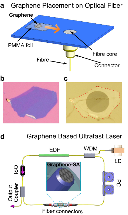
We developed a procedure for deterministic placement, following transfer. This exploits a water layer between the PMMA/graphene foil and the substrate, enabling the PMMA to move. This allows to place graphene layers on any substrate in any predefined location, prepare ”artificial” multi-layers, create sandwich structures with other materials (such as BN, MoS2), etc. We will show an example of this technique in Section IV.7, by placing graphene on the core of an optical fibre.
Large scale placement of LPE samples can be achieved by spin coating and Langmuir-BlogdettDai_nnano , even though with lack of positional control. Surface modification by self-assembled monolayers (SAMs) can enable targeted deposition of graphene flakes in a large scale. Di-electrophoresis allows controlled placement of individual graphene flakes between pre-patterned electrodeskrupke . Inkjet printing is another attractive techniqueBeecher_JAP , and could directly ”write” optoelectronic devices.
IV Photonics and Optoelectronics applications
IV.1 Transparent conductors
Optoelectronic devices such as displays, touch-screens, light emitting diodes, solar cells, require materials with low sheet resistance and high transparency. In a thin-film /d, where d is the film thickness and the resistivity. For a rectangle of length L and width W, the resistance R is:
| (5) |
The term L/W can be seen as the number of squares of side W that can be superimposed on the resistor without overlapping. Thus, even if Rs has units of ohms as R, it is historically quoted in ”ohms per square” ().
Current transparent conductors (TC) are semiconductor-basedHamberg_JAP_1986 : doped Indium Oxide (In2O3)Holland_53 , Zinc Oxide (ZnO)Minami_SST_2005 , Tin Oxide (SnO2)Hamberg_JAP_1986 , as well as ternary compounds based on their combinationsHamberg_JAP_1986 ; Minami_SST_2005 ; Granqvist_07 . The dominant material is indium tin-oxide (ITO), a doped n-type semiconductor composed of In2O3, and SnO2Hamberg_JAP_1986 . The electrical and optical properties of ITO are strongly affected by the impuritiesHamberg_JAP_1986 . Sn atoms act as n-type donorsHamberg_JAP_1986 . ITO has strong absorption above 4eV due to interband transitionsHamberg_JAP_1986 , with other features at lower energy related to scattering of free electrons with Sn atoms or grain boundariesHamberg_JAP_1986 . ITO is commercially available with T and as low as on glassMinami_SST_2005 , and on polyethylene terephthalate (PET)Granqvist_07 . Note that T is typically quoted at 550nm, since this is where the human eye spectral response is maximumHamberg_JAP_1986 .
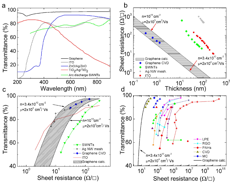
ITO suffers severe limitations: an ever increasing cost due to Indium scarcityHamberg_JAP_1986 , processing requirements, difficulties in patterningGranqvist_07 ; Hamberg_JAP_1986 , sensitivity to acidic and basic environments. Moreover, ITO is brittle and can easily wear out or crack when used in applications where bending is involved, such as touch screens and flexible displayssheraw_02 . This demands new TC materials with improved performance. Metal gridsPeumans_NL , metallic nanowiresDe_acsnano2 , or other metal oxidesGranqvist_07 have been explored as alternative. Nanotubes and graphene also show great promise. In particular, graphene films have higher T over a wider wavelength range with respect to SWNT filmsGeng_JACS ; Wu_NT_Science ; Coleman_ACS , thin metallic filmsPeumans_NL ; De_acsnano2 , and ITOHamberg_JAP_1986 ; Minami_SST_2005 , Fig. 2a.
We now give a relation between T and Rs for graphene films of varying doping. From Eq. 4, T depends on the optical conductivity G0,
| (6) |
where N is the number of layers. Rs is linked to the bi-dimensional dc conductivity by:
| (7) |
Combining Eqs. 6,7, eliminating N, gives:
| (8) |
where, =377 is the free space impedance, being the free space electric constant and c the speed of light. In SLG we can take , where n is the number of charge carriersGeim_nmat . Note that for n0, does not go to zero, but assumes a constant valueGeim_nmat , resulting in Rs6k for an ideal intrinsic SLG with T. Thus, ideal intrinsic SLG, would beat the best ITO only in terms of T, not Rs. However, samples deposited on substrates, or in thin films, or embedded in polymers are never intrinsic. Exfoliated SLG has typically n (see e.g. Ref. Casi_APL, ), and much smaller Rs. The range of T and that can be realistically achieved for graphene layers of varying thickness can be estimated taking n=1012-10 and =103-2104cm2/Vs, as typical for CVD grown films. Figs. 2b,c show that graphene can achieve the same as ITO, ZnO-Ag-ZnOSahu_ASS , TiO2/Ag/TiO2 and SWNTs with a similar or even higher T. Fig. 2c plots T versus for ITOPeumans_NL , Ag nanowiresPeumans_NL , SWNTsGeng_JACS and the best graphene-based transparent conductive film (TCFs) reported to dateBae_arxiv , again showing that the latter is superior. For instance, taking n=3.41012cm-2 and =2104cm2/Vs, we get T=90 and . Note that Eq.8 is intended as guideline for TCF design and optimization, not as a statement on the transport physics of graphene. For TCF design empirical expressions of as a function of carrier concentration and doping are enough, whatever the origin and precise quantification of the minimal conductivity, and of the dependence of Rs on doping, defects, electron-hole puddles, etc.
Different strategies were explored to prepare graphene-based TCFs (GTCFs): sprayingGilje_Nanoletters , dipWang_NL and spin coatingBecerril_ACSnano , vacuum filtrationEda_nnano , roll-to-roll processingBae_arxiv .
Significant progress was made since the first attempts to produce GO based TCFs (GOTCFs). Since GO is insulating, it must be reduced to improve Stankovich_Nature . Ref. Gilje_Nanoletters, decreased from to following reduction with dimethylhydrazine. GraphitizationBecerril_ACSnano , hydrazine exposure and low-temperature annealingEda_nnano , or high-temperature vacuum annealingWuACSnano further decreased , down to for T=82%WuACSnano .
Dispersions of graphite intercalated compounds (GIC)Biswas_NL and hybrid nanocomposites (GO sheets mixed with silica sols or CNTsTung_NL ) were also attempted, with a minimum for T=Tung_NL . Graphene films produced by chemical synthesis, currently show for T=Wang_Angwandte .
Ref. Blake_nanoletters, reported, thus far, the best GTCF from LPE of graphite. This was fabricated by vacuum filtration, followed by annealing, achieving Rs=; T. The high is most likely due to the small flake size, and lack of percolationBlake_nanoletters ; Green_NL . The role of percolation can be seen in Ref. Green_NL, , where and T went from ;; to , increasing flake size.
A key strategy to improve performance is stable chemical doping. Ref. Blake_nanoletters, prepared GTCFs, produced by MC, with T;=, exploiting a layer of polyvinyl alcohol (PVA) to induce n-type doping. Ref. Bae_arxiv, achieved Rs;T by nitric acid treatment of GTCFs derived from CVD grown flakes, one order of magnitude lower in terms of than previous GTCFs from wet transfer of CVD filmsKim_nature .
Figure 2d is an overview of current GTCFs and GOTCFs. It shows that GTCFs derived from CVD flakes, combined with doping, could outperform ITO, metal wires and SWNTs. Note that GTCFs and GOTCFs produced by other methods, such as LPE, albeit presently with higher at T=90, have already been tested in organic light emittersWuACSnano ; Matyba_Acsnano and solar cellsWang_NL ; Liu_AM . These are a cheaper and easier scalable alternative to MC or CVD films, and need be considered in applications where cost reduction is crucial.
IV.2 Photovoltaic devices
A photovoltaic (PV) cell converts light to electricityChapin_1954 . ISC is the maximum short circuit current, while VOC is the maximum open circuit voltage. The fill factor (FF) is defined as: FF=(VmaxImax)/(VOCISC), where and are maximum voltage and current. The energy conversion efficiency is =Pmax/Pinc, where and is the incident power. The fraction of absorbed photons converted to current defines the internal photocurrent efficiency (IPCE).
Current PV technology is dominated by Si cellsChapin_1954 , with up to25 Green_2001 . Organic photovoltaic cells (OPVs) rely on polymers for light absorption and charge transportHoppe_04 . They can be manufactured economically compared to Si-cells, for example by a roll-to-roll processKreebs_09 , even though they have lower . An OPV consists of a TC, a photoactive layer and the electrodeHoppe_04 . Dye-sensitized solar cells (DSSCs) use a liquid electrolyte as a charge transport mediumGratzel_Nature . A DSSC consists of a high porosity nanocrystalline photoanode, comprising TiO2 and dye molecules, both deposited on a TCGratzel_Nature . When illuminated, the dye molecules capture the incident photon generating electron/holes pairs. The electrons are injected into the conduction band of the TiO2 and transported to the counter electrode, the cathodeGratzel_Nature . Regeneration of dye molecules is accomplished by capturing electrons from a liquid electrolyte. Presently, ITO is the most common material used both as photoanode and cathode, the latter with a Pt coating.
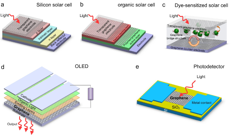
Graphene can fulfill multiple functions in PV devices: 1) TC window, 2) photoactive material, 3) channel for charge transport, 4) catalyst.
GTCFs can be used as window electrodes in inorganic (Fig. 3a), organic (Fig.3b), and DSSCs devices (Fig. 3c). Ref. Wang_Angwandte, used GTCFs produced by chemical synthesis, reporting . Higher was achieved using reduced GOWu_APL , having Wu_APL instead of Wang_Angwandte , despite a lower T ( instead of ). Ref. De_Arco, achieved better performance () using CVD graphene as TCs with and T=72. Further optimization is certainly possible, considering the performance of the best GTCF to dateBae_arxiv .
GO dispersions were also used in bulk hetero-junction PV devices, as electron-acceptors with poly(3-hexylthiophene) and poly(3-octylthiophene) as donors, with Liu_AM . Ref. Yong_Small, claims that should be possible with graphene as photoactive material.
Graphene can cover an even larger number of functions in DSSCs. Ref. Wang_NL, reported a solid-state DSSC based on spiro-OMeTAD1 (as hole transport material) and porous TiO2 (for electron transport) using a GTCF anode, with . Graphene can be incorporated into the nanostructured TiO2 photoanode to enhance the charge transport rate, preventing recombination, thus improving the IPCEYang_acsnano . Ref. Yang_acsnano, used graphene as TiO2 bridge, achieving faster electron transport and lower recombination, leading to , higher than conventional nanocrystalline TiO2 photoanodesYang_acsnano . Another option is to use graphene to substitute the Pt counter electrode, due to its high specific surface area. An hybrid poly(3,4-ethylenedioxythiophene (PEDOT):poly-(styrenesulfonate) (PSS)/GO composite was used as counter electrode, getting =4.5, comparable to 6.3, for a Pt counter electrode tested under the same conditionsHong_el_comm , but now with a cheaper material.
IV.3 Light-emitting devices
Organic light-emitting diodes (OLED) have an electroluminescent layer between two charge-injecting electrodes, at least one of which transparentFriend_Nature . In OLED, holes are injected into the highest occupied molecular orbital (HOMO) of the polymer from the anode, while electrons are injected into the lowest unoccupied molecular orbital (LUMO) from the cathode. For efficiently injection, the anode and cathode work functions should match the HOMO and LUMO of the light-emitting polymerFriend_Nature . Due to the image quality, low power consumption and ultra-thin device structure, OLEDs find applications in ultra-thin televisions and other display screens, such as computer monitors, digital cameras and mobile phones. Traditionally, ITO, having a work function 4.4-4.5eV, is used as TCF. However, besides cost issues, ITO is brittle and limited as flexible substrateGranqvist_07 . Also, In tends to diffuse into the active OLED layers, leading to a reduction of performance over timeHamberg_JAP_1986 . Thus, there is a need for alternative TCFs with optical and electrical performance similar to ITO, but without its drawbacks. Graphene has a work function of 4.5eVGiovannetti_PRL , similar to ITO. This, combined with its promise as flexible and cheap TCF, makes it an ideal candidate as OLED anode, Fig. 3d, eliminating at the same time the issues related to In diffusion. GTCFs anodes enabled out-coupling efficiency comparable to ITOWuACSnano . Considering that and T were and 82 at 550nmWuACSnano , it is reasonable to expect further optimization will improve performance.
Ref. Matyba_Acsnano, used a GOTCF in a light-emitting electrochemical cell (LEC). This is a device, similar to an OLED, where the light-emitting polymer is blended with an electrolytePei_Nat_Mat . The mobile ions in the electrolyte rearrange when a potential is applied between the electrodes, forming high charge-density layers at each electrode interface, allowing efficient and balanced injection of electrons and holes, regardless of the work function of the electrodesPei_Nat_Mat . Usually, LECs have at least one metal electrode. Electrochemical side-reactions, involving the electrode materials, can cause problems in terms of operational lifetime and efficiencyMatyba_Acsnano . This also hinders the development of flexible LEC devices. Graphene is the ideal material to overcome these problems. Ref. Matyba_Acsnano, demonstrated a LEC based solely on dispersion-processable carbon-based materials, paving the way to totally organic low-voltage, inexpensive, and efficient LEDs.
IV.4 Photodetectors
Photodetectors (PDs) measure photon flux or optical power by converting the absorbed photon energy into electrical current. They are widely used in a range of common devicesSaleh_book , such as remote controls, TVs, DVD players, etc. Most PDs exploit the internal photo-effect, where the absorption of photons results in carriers excited from the valence to the conduction band, outputting an electric current. The spectral bandwidth is typically limited by the material absorptionSaleh_book . For example, PDs based on IV and III-V semiconductors suffer from the so-called ”long-wavelength limit”, as these become transparent when the incident energy is smaller than the bandgapSaleh_book . Graphene absorbs from UV to THzNair_Science ; Sun_graphene ; Dawlaty_APL_2 ; Wright_PRL . As a result, graphene based PDs (GPDs) (see Fig. 3e) could work over a much broader wavelength range. The response time is ruled by the carrier mobilitySaleh_book . Graphene has huge mobilities. Hence, GPDs can be ultrafast.
The photoelectrical response of graphene has been widely investigated, both experimentally and theoreticallyVasko_PRB_08 ; Park_2009_NL ; Xia_NL_2009 ; Xia_nnano ; Mueller_NP_10 . Photoelectrical response at 0.514, 0.633, 1.5 and 2.4m was reportedMueller_NP_10 . Much broader spectral detection is expected due to the graphene ultrawideband absorption. Ref. Xia_nnano, demonstrated a GPD with photo-response up to 40GHz. The GPD operation bandwidth is mainly limited by the time constant resulting from the device resistance R and capacitance C. Ref. Xia_nnano, , reported a RC limited bandwidthGHz, comparable to traditional PDsKang_NP_09 . However, the maximum possible operation bandwidth of PDs is typically restricted by the transit time, the finite duration of the photo-generated current Saleh_book . The transit time limited bandwidth of a GPD could be well over 1500GHz Xia_nnano , surpassing state-of-the-art PDs.
Although external electric field can produce efficient photocurrent generation, with electron-hole separation efficiencyPark_2009_NL , zero source-drain bias and dark current operations could be achieved by using the internal electric field formed near the metal electrode-graphene interfacesXia_nnano ; Mueller_NP_10 . The small effective area of the internal electric field could decrease the detection efficiencyXia_nnano ; Mueller_NP_10 , since most of the generated electron-hole pairs would be out of the electric field, thus recombining, rather than being separated. The IPCE ()Xia_NL_2009 ; Park_2009_NL and external responsivity (generated electric current for given input optical power) of 6.1mA/WMueller_NP_10 so far reported for GPDs are relatively low compared to current PDsSaleh_book . This is mainly due to limited optical absorption when only one SLG is used, short photo-carrier lifetime, and small effective photo-detection area ( in Ref. Xia_nnano, ).
The photo-thermoelectric effect, which exploits the conversion of photon energy into heat and then electric signalSaleh_book , may play an important role in photocurrent generation in graphene devicesPark_2009_NL ; Xu_NL_10 . Thus photo-thermoelectric GPDs may be possible.
IV.5 Touch screens
Touch screens are visual outputs that can detect the presence and location of a touch, by a finger or other objects, such as a pen, within the display area, thereby permitting the physical interaction with what shown on the display itselfMaeda_99 . Touch panels are currently used in a wide range of applications, such as cellular phones and digital cameras, and where keyboard and mouse do not allow a satisfactory, intuitive, quick, or accurate interaction by the user with the display content.
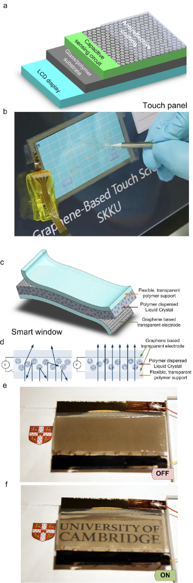
Resistive and capacitive (see Fig. 4a) touch panels are the most common. A resistive touch panel comprises a conductive substrate, a liquid crystal device (LCD) frontpanel, and a TCFMaeda_99 . When pressed by a finger or pen, the frontpanel film comes into contact with the bottom TC and the coordinates of the contact point are calculated on the basis of their resistance values. There are two categories of resistive touch screens: matrix and analogueMaeda_99 . The matrix has striped electrodes, while the analogue has a non-patterned TC electrode, thus lower production costs. The TC requirements for resistive screens are and T90 at 550nmMaeda_99 . Favorable mechanical properties, including brittleness and wear resistance, high chemical durability, no toxicity, and low production costs are also important. Cost, brittleness, wear resistance, and chemical durability are the main limitations of ITOHamberg_JAP_1986 ; Granqvist_07 . Thus for resistive touch-screens there is an effort to find an alternative TC. Indeed, ITO cannot withstand repeated flexing and poking involved with this type of touch screens without cracking or deteriorating.
GTCFs can satisfy the requirements for resistive touch screens in terms of T and , when combined with large area uniformity. Ref. Bae_arxiv, recently reported a graphene-based touch panel display by screen-printing a CVD grown sample, Fig. 4b. Considering the and T required by analogue resistive screens, GTCF or GOTCF produced via LPE also offer a viable alternative, and further cost reduction.
Capacitive touch screens are emerging as the high-end version, especially since the launch of Apple’s iPhone. These consist of an insulator such as glass, coated with ITOMaeda_99 . As the human body is also a conductor, touching the surface of the screen results in a electrostatic field distortion, measurable as a change in capacitance. Although capacitive touch screens do not work by poking with a pen, thus mechanical stresses are lower with respect to resistive ones, the use of GTCFs can improve performance and reduce costs.
IV.6 Flexible smart windows
Polymer dispersed liquid crystal devices (PDLC) or similar structures, generally known as ’smart windows’, were introduced in the early 80scraighead_82 . These consist of thin films of optically transparent polymers with micron-sized LC droplets contained within pores of the polymer. Light passing through the LC/polymer is strongly forward scattered, producing a milky filmdrzaic_86 ; doane_88 . If the LC ordinary refractive index is close to that of the host polymer, the application of an electric field results in a transparent statesheraw_02 . The ability of switching from translucent to opaque makes them attractive in many applications, e.g. where privacy at certain times is highly desirable. There are other potential applications of PDLC in flexible displays due to their compatibility with flexible substrates and wide viewing anglesheraw_02 . For example, Ref. sheraw_02, demonstrated an organic thin film transistor driven flexible display with each individual pixel controlled by an addressable PDLC matrix. Conventionally, ITO on glass is used as TCF to apply the electric field across the PDLC. However, one of the reasons behind the limited market penetration of smart windows is the significant ITO cost. Furthermore, flexibility is hindered when using ITO, reducing potential applications, such as PDLC flexible displayssheraw_02 . For transparent or colored/tinted smart windows, the generally required T and range from 60 to 90 and above and 100 to 1k depending on production cost, application and manufacturer. In addition to flexibility, the electrodes need to be as large as the window itself and must have long term physical and chemical stability, as well as being compatible with the roll to roll PDLC production process.
All these deficiencies of ITO electrodes can be overcome by GTCFs. Figures 4c,d shows the working principle and Fig. 4e,f a prototype of a flexible smart window with PET used as substrate.
IV.7 Saturable absorbers and ultrafast lasers
Materials with non-linear optical and electro-optical properties are needed in most photonic applicationsBoyd_book ; Hasan_AM . Laser sources producing nano- to sub-picosecond pulses are a major component in the portfolio of leading laser manufacturers. Thus far, solid-state lasers are the short-pulse source of choice, being deployed in a variety of applications ranging from basic research to material processing, from eye surgery to printed circuit board manufacturing, from metrology to trimming of electronic components such as resistors and capacitors. Regardless of wavelength, the majority of ultrafast laser systems employ a mode-locking technique, whereby a non-linear optical element, called saturable absorber (SA), turns the continuous wave output into a train of ultrafast optical pulsesKeller_nature_03 . The key requirements for non-linear materials are fast response time, strong non-linearity, broad wavelength range, low optical loss, high power handling, low power consumption, low cost and ease of integration into an optical system. Currently, the dominant technology is based on semiconductor saturable absorber mirrors (SESAMs)Keller_nature_03 . However, these have a narrow tuning range, and require complex fabrication and packaging Keller_nature_03 ; Hasan_AM . A simple, cost-effective alternative is to use SWNTsHasan_AM ; Wang_Tunable , where the diameter controls the gap, thus the operating wavelength. Broadband tunability is possible using SWNTs with a wide diameter distributionHasan_AM ; Wang_Tunable . However, when operating at a particular wavelength, SWNTs not in resonance are not used and contribute unwanted losses.
As discussed in Sect.II.3, the linear dispersion of the Dirac electrons in graphene offers an ideal solution: for any excitation there is always an electron-hole pair in resonance. The ultrafast carrier dynamicsBreusing_PRL ; SUN_PRL , combined with large absorption and Pauli blocking make graphene an ideal ultra-broadband, fast SA. Compared to SESAMs and SWNTs, there is no need of bandgap engineering or chirality/diameter control.
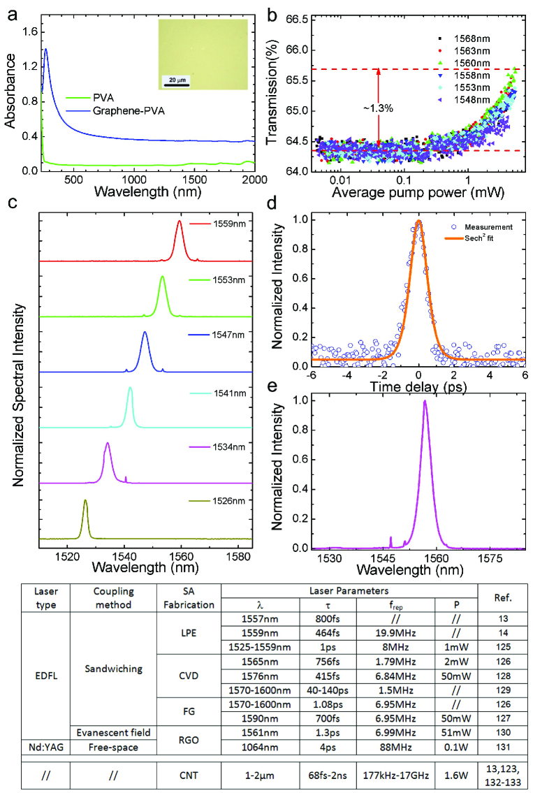
Thus far, graphene-polymer compositesHasan_AM ; Sun_graphene ; Sun_Tunable ; Bao_AFM_2010 ; Zhang_APL_gra , CVD grown filmsZhang_OE_gra ; Zhang_apl_10_tun , functionalized graphene (e.g. GO bonded with poly[(m-phenylenevinylene)-co-(2,5-dioctoxy-p-phenylenevinylene)])Bao_AFM_2010 and reduced GO flakesSong_APL_2010 ; Tan_APL_2010 were used for ultrafast lasers. Graphene-polymer composites are scalable and, more importantly, allow easy integration into a range of photonic systemsHasan_AM ; Sun_graphene ; Sun_Tunable . Another route for graphene integration is via deterministic placement in a pre-defined position on a substrate of choice, e.g. a fiber core or cavity mirrors. Fig.5a shows such transfer of a flake onto an optical fibre core. This is achieved by exploiting a water layer between the poly(methyl methacrylate)(PMMA)/graphene foil and the optical fibre, which enables the PMMA to move. Graphene integration is finally obtained after precise alignment to the fibre core by a micro-manipulator (Fig. 5 b) and dissolution of the PMMA layer (Fig.5c).
A typical absorption spectrum is shown in Fig.6a Hasan_AM ; Sun_graphene ; Sun_Tunable . This is featureless, save a characteristic UV plasmon peak, while the host polymer only contributes a small background for longer wavelengths. Fig.6b plots T as a function of average pump power at six wavelengths. Saturable absorption is evident by the T increase with power at all wavelengths.
Various strategies have been proposed to integrate graphene saturable absorbers (GSAs) in laser cavities for ultrafast pulse generation. The most common is to sandwich a GSA between two fibre connectors with a fibre adapter, as schematized in Fig.5c Hasan_AM ; Sun_graphene ; Sun_Tunable . Graphene on a side-polished fiber was also reported, aimed at high power generation by evanescent field interactionSong_APL_2010 . A quartz substrate coated with graphene was used for free-space solid-state lasersTan_APL_2010 .
The most common wavelength of generated ultrafast pulses so far is, since this is the standard in optical telecommunications, not because GSAs have any preference for a particular wavelength. A solid-state laser mode-locked by graphene was reported atTan_APL_2010 . Fig.6c shows a GSA-mode locked EDF laser tuneable from 1526 to 1559nmSun_Tunable , with the tuning range mainly limited by the tunable filter, not the GSA. Fig.6d,e show the pulse from a GO based saturable absorber (GOSA). The possibility of tuning the GSA properties by functionalization and using different layers or composite concentrations, offers considerable design freedom. Fig.6 has a table comparing the performance of graphene-based ultrafast lasers and the main CNT-based devicesScardaci_am_2008 ; Sun_apl_2009 .
IV.8 Optical limiters
Optical limiters (OL) are devices with high transmittance for low incident light intensity, and vice-versa for high intensityBass_book . There is a great interest in OL mainly for optical sensors and human eye protectionBass_book , as damage can happen when the intensity exceeds a thresholdBass_book . Passive OL using a nonlinear optical material, have potential for simplicity, compactness and low costBass_book . However, so far there is no demonstration of passive OL able to protect eyes and other common sensors over the entire visible and NIR rangeBass_book . Typical OL materials include semiconductors (e.g. ZnSe, InSb), organic molecules (e.g. phthalocyanines), LC and carbon based composites (e.g. carbon-black dispersions, CNTs, fullerenes)Bass_book ; Wang_advmater . Fullerenes and their derivativesTutt_Nat_92 ; Wang_jmc_09 and CNTs dispersionsWang_jmc_09 have good OL performance, in particular for ns pulses at 532 and 1064nmWang_jmc_09 .
In graphene-based OL the absorbed light energy converts into heat, creating bubbles and microplasmasWang_advmater , resulting in reduced transmission. Graphene dispersions can be used as wideband OL covering visible and NIR. Broad OL (from 532 to 1064nm) of LPE graphene was reported for ns pulsesWang_advmater . It was shown that funtionalized graphene dispersions could outperform Xu_AM_2009 .
IV.9 Optical Frequency converters
Optical frequency converters are used to expand the wavelength accessibility of lasers (e.g. frequency doubling, parametric amplification and oscillation, and four-wave mixing (FWM))Bass_book . Calculations suggest that nonlinear frequency generation in graphene (e.g. harmonics of input light) should be possible for sufficiently high external electric field ()Mikhailov_EPL_2007 . Second harmonic generation (SHG) from a 150fs laser at 800nm was reported for a graphene filmDean_APL_2009 . In addition, FWM, generating NIR wavelength-tunable light was demonstrated using SLG and FLGHendry_2009_FWM . Graphene’s third-order susceptibility was measured to be Hendry_2009_FWM , one order of magnitude larger than reported so far for CNTs Hendry_2009_FWM . However, photon-counting electronics is typically needed to measure the outputDean_APL_2009 , indicating a low conversion efficiency. Other features of graphene, such as the possibility of tuning the nonlinearity by changing the number of layersHendry_2009_FWM , and wavelength-independent nonlinear susceptibilityHendry_2009_FWM , still could be potentially used for various photonic applications (e.g. optical imaging Hendry_2009_FWM ).
IV.10 THz devices
THz radiation in the 0.3 to 10THz range ( to ), is attractive for biomedical imaging, security, remote sensing and spectroscopyThz_book . A large amount of unexplored territory for THz technology still remains mainly due to a lack of affordable and efficient THz sources and detectorsThz_book . The frequency of graphene plasma wavesRana_2008 ; Ryzhii_JAP_07_1 lies in the THz range, as well as the gap of GNRs, and the BLG tunable band gap, making graphene appealing for THz generation and detection. Various THz sources were suggested, based on electricalRana_2008 ; Ryzhii_JAP_07_1 or opticalRana_2008 ; Ryzhii_JAP_07_1 pump of graphene devices. Recent experimental observations of THz emissionSun_NL_10 and amplificationOtsuji_10_THz in optically pumped graphene show the feasibility of graphene-based THz generation. Twisted multilayers, retaining the electronic properties of SLG, could also be interesting for THz applications.
Graphene devices can be used for THz detection and frequency conversion. The possibility of tuning the electric and optical properties by external means (e.g. electric and magnetic field, optical pump), makes SLG and FLG suitable for IR and THz radiation manipulation as well. The possible devices include modulators, filters, switches, beam splitters and polarizers.
V Perspective
Graphene films and composites have attractive electronic and optical properties, making them ideal for photonics and optoelectronics. A number of applications are enabled by using graphene as a replacement for ITO and other transparent conductors. In many cases (e.g. touch-screens, OLEDs) this also adds fabrication flexibility, in addition to economic advantages. Current PDLC-based devices face major challenges due to fabrication costs associated with the requirement of large transparent electrodes. The move to a graphene-based technology could make them more viable. Novel graphene-based transparent electrodes on flexible substrates for solar cells can add value and operational flexibility, not possible with current transparent conductors and rigid glass substrates. Recent progresses on growth and dispersion processing of graphene have definitely made this material ”come of age”, encouraging industrial applications. Deterministic placement of graphene layers on arbitrary substrates, and multi-layers by individual assembly of monolayers at given angles are now possible. Future efforts on nonlinear optical devices will focus on demonstrators at different wavelengths to fully exploit graphene’s ultrawide broadband capability. Ultrafast and tunable lasers are a reality, with an ever growing number of groups entering this field. The combination of graphene photonics with plasmonics could enable a variety of advanced devices.
VI Acknowledgments
We thank S. A. Awan, D.M. Basko, E. Lidorikis, A. Hartschuh, J. Coleman, A. Dyadyusha, T. Kulmala, A. Lombardo, D. Popa, G. Privitera, F. Torrisi, O. Trushkevych, F. Wang, T. Seyller,B. H. Hong, A.K. Geim, K.S. Novoselov for useful discussions. We acknowledge funding from EPSRC grants GR/S97613/01, EP/E500935/1, ERC grant NANOPOTS, a Royal Society Brian Mercer Award for Innovation, the Cambridge Integrated Knowledge Centre in Advanced Manufacturing Technology for Photonics and Electronics. F.B. acknowledges funding from a Newton International Fellowship and T.H. from King’s College, Cambridge. A.C.F. is a Royal Society Wolfson Research Merit Award holder.
References
- (1) A. K. Geim, K. S. Novoselov, Nat. Mater. 6, 183 (2007).
- (2) J.C. Charlier, P. C. Eklund, J. Zhu ,Ferrari, A. C., Electron, Top. Appl. Phys. 111, 673 (2008).
- (3) P. R. Wallace, Phys. Rev. 71, 622 (1947).
- (4) Y. Zhang, Y. W. Tan, H. L. Stormer, P. Kim, Nature 438, 201 (2005).
- (5) X. Du, I. Skachko, F. Duerr, A. Luican, E. Y. Andrei, Nature 462, 192 (2009).
- (6) M. C. Lemme, T. J. Echtermeyer, M. Baus, H. Kurz, IEEE Electr. Dev. Lett. 28, 282 (2007).
- (7) M. Y. Han, B. Ozyilmaz, Y. Zhang, P. Kim, Phys. Rev. Lett. 98, 206805 (2007).
- (8) Y. M. Lin, C. Dimitrakopoulos, K. A. Jenkins, D. B. Farmer, H. Y. Chiu, A. Grill, P. Avouris, Science 327, 662 (2010).
- (9) C. Casiraghi, A. Hartschuh, E. Lidorikis, H. Qian, H. Harutyunyan, T. Gokus, K. S. Novoselov, A. C. Ferrari, Nano Lett. 7, 2711 (2007).
- (10) P. Blake, E. W. Hill, A. H. C. Neto, K. S. Novoselov, D. Jiang, R. Yang, T. J. Booth, A. K. Geim, Appl. Phys. Lett. 91, 063124 (2007).
- (11) R. R. Nair, P. Blake, A. N. Grigorenko, K. S. Novoselov, T. J. Booth, T. Stauber, N. M. R. Peres, A. K. Geim, Science 320, 1308 (2008).
- (12) V. G. Kravets, A. N. Grigorenko, R. R. Nair, P. Blake, S. Anissimova, K. S. Novoselov, A. K. Geim, Phys. Rev. B 81, 155413 (2010).
- (13) T. Hasan, Z. Sun, F. Wang, F. Bonaccorso, P. H. Tan, A. G. Rozhin, A. C. Ferrari, Adv. Mater. 21, 3874 (2009).
- (14) Z. Sun, T. Hasan, F. Torrisi, D. Popa, G. Privitera, F. Wang, F. Bonaccorso, D. M. Basko, A. C. Ferrari, ACS Nano 4, 803 (2009).
- (15) C. H. Lui, et al. Light Emission from Graphene Induced by Femtosecond Laser Pulses, APS March (2010);S. Wu, et al. Nonlinear photoluminescence from graphene. APS March 2010; R. Stohr, et al. What is the color of graphene, Black and dark or white and bright?. DPG Fruhjahrstagung Regensburg, (2010); A. Hartschuh et al. Excited State Energies and Decay Dynamics in Carbon Nanotubes and Graphene, E-MRS Spring Meeting 2010.
- (16) T. Gokus, R. R. Nair, A. Bonetti, M. Bohmler, A. Lombardo, K. S. Novoselov, A. K. Geim, A. C. Ferrari, A. Hartschuh, ACS Nano 3, 3963 (2009).
- (17) G. Eda, Y. Y. Lin, C. Mattevi, H. Yamaguchi, H. A. Chen, I. S. Chen, C. W. Chen, M. Chhowalla, Adv. Mater. 22, 505 (2009).
- (18) X. Sun, Z. Liu, K. Welsher, J. T. Robinson, A. Goodwin, S. Zaric, H. Dai, Nano Res. 1, 203 (2008).
- (19) Z. Luo, P. M. Vora, E. J. Mele, A. T. C. Johnson, J. M. Kikkawa, Appl. Phys. Lett. 94, 111909 (2009).
- (20) A. B. Kuzmenko, E. van Heumen, F. Carbone, D. van der Marel, Phys. Rev. Lett. 100, 117401 (2008).
- (21) F. Wang, Y. B. Zhang, C. S. Tian, C. Girit, A. Zettl, M. Crommie, Y. R. Shen, Science 320, 206 (2008).
- (22) K. F. Mak,M. Y. Sfeir,J. A. Misewich,T.F. Heinz, arXiv:0908.0154 (2009); K. F. Mak,J. Shan,T. F. Heinz, Phys. Rev. Lett. 104, 176404 (2009)
- (23) M. Breusing, C. Ropers, T. Elsaesser, Phys. Rev. Lett. 102, 086809 (2009).
- (24) T. Kampfrath, L. Perfetti, F. Schapper, C. Frischkorn, M. Wolf, Phys. Rev. Lett. 95, 187403 (2005).
- (25) M. Lazzeri, S. Piscanec, F. Mauri, A. C. Ferrari, J. Robertson, Phys. Rev. Lett. 95, 236802 (2005).
- (26) J. Gonzalez, F. Guinea, M. A. H. Vozmediano, Phys. Rev. Lett. 77, 3589 (1996).
- (27) J. Lu, J. X. Yang, J. Wang, A. Lim, S. Wang, K. P. Loh, ACS Nano 3, 2367 (2009).
- (28) J. R. Sheats, H. Antoniadis, M. Hueschen, W. Leonard, J. Miller, M. Ron, D. Roitman, A. Stocking, Science 273, 884 (1996).
- (29) L.J.Rothberg, A.J.Lovinger, J.Mat.Res. 11, 3174 (1996).
- (30) J. V. Frangioni, Curr Opin Chem Biol. 7, 626 (2003).
- (31) S. Essig, C. W. Marquardt, A. Vijayaraghavan, M. Ganzhorn, S. Dehm, F. Hennrich, F. Ou, A. A. Green, C. Sciascia, F. Bonaccorso, K. P. Bohnen, H. V. Lohneysen, M. M. Kappes, P. M. Ajayan, M. C. Hersam, A. C. Ferrari, R. Krupke, Nano Lett. 10, 1589 (2010).
- (32) K. S. Novoselov, D. Jiang, F. Schedin, T. J. Booth, V. V. Khotkevich, S. V. Morozov, A. K. Geim, PNAS 102, 10451 (2005).
- (33) A. E. Karu, M. Beer, J. Appl. Phys. 37, 2179 (1966).
- (34) A. N. Obraztsov, E. A. Obraztsova, A. V. Tyurnina, A. A. Zolotukhin, Carbon 45, 2017 (2007).
- (35) K. S. Kim, Y. Zhao, H. Jang, S. Y. Lee, J. M. Kim, K. S. Kim, J. H. Ahn, P. Kim, J. Y. Choi, B. H. Hong, Nature 457, 706 (2009).
- (36) A. Reina, X. Jia, J. Ho, D. Nezich, H. Son,V.Bulovic,M.S. Dresselhaus,J.Kong, Nano Lett. 9,30 (2009)
- (37) S. Bae, H. K. Kim, X. Xu, J. Balakrishnan, T. Lei, Y. I. Song, Y. J. Kim, B. Ozyilmaz, J.-H. Ahn, B. H. Hong, S. Iijima, arXiv , 0912.5485v1 (2009); Nat. Nano. (2010)
- (38) C. Berger, Z. M. Song, T. B. Li, X. B. Li, A. Y. Ogbazghi, R. Feng, Z. T. Dai, A. N. Marchenkov, E. H. Conrad,P.N. First,W.A. de Heer,J. Phys. Chem. B 108,19912 (2004)
- (39) P. W. Sutter,J.I. Flege,E.A. Sutter,Nat. Mat. 7,406 (2008)
- (40) K. V. Emtsev, A. Bostwick, K. Horn, J. Jobst, G. L. Kellogg, L. Ley, J. L. McChesney, T. Ohta, S. A. Reshanov, J. Rohrl, E. Rotenberg, A. K. Schmid, D. Waldmann, H. B. Weber, T. Seyller, Nat. Mater. 8, 203 (2009).
- (41) X. Li, X. Wang, L. Zhang, S. Lee, H. Dai, Science 319, 1229 (2008).
- (42) Y. Hernandez, V. Nicolosi, M. Lotya, F. M. Blighe, Z. Sun, S. De, I. T. McGovern, B. Holland, M. Byrne, Y. K. Gunko, J. J. Boland, P. Niraj, G. Duesberg, S. Krishnamurthy, R. Goodhue, J. Hutchison, V. Scardaci, A. C. Ferrari, and J. N. Coleman, Nat. Nanotech. 3, 563 (2008).
- (43) M. Lotya, Y. Hernandez, P. J. King, R. J. Smith, V. Nicolosi, L. S. Karlsson, F. M. Blighe, S. De, Z. Wang, I. T. McGovern, G. S. Duesberg, J. N. Coleman, J. Am. Chem. Soc. 131, 3611 (2009).
- (44) C. Valles, C. Drummond, H. Saadaoui, C. A. Furtado, M. He, O. Roubeau, L. Ortolani, M. Monthioux, A. Penicaud, J. Am. Chem. Soc. 130, 15802 (2008).
- (45) S. Stankovich, D. A. Dikin, G. H. B. Dommett, K. M. Kohlhaas, E. J. Zimney, E. A. Stach, R. D. Piner, S. T. Nguyen, R. S. Ruoff, Nature 442, 282 (2006).
- (46) O.M. Marago, F. Bonaccorso, R. Saija, G.Privitera, P.G. Gucciardi, M.A. Iati, G. Calogero, P.H. Jones, F. Borghese,P.Denti,V.Nicolosi,A.C. Ferrari, arXiv1006.0280v1 (2010).
- (47) A. A. Green, M. C. Hersam, Nano Lett. 9, 4031 (2009).
- (48) X. Li, G. Zhang, X. Bai, X. Sun, X. Wang, E. Wang, H. Dai, Nat. Nanotech. 3, 538 (2008).
- (49) W. S. Hummers, R. E. Offeman, JACS 80, 1339 (1958).
- (50) B. C. Brodie, Ann. Chim. Phys. 59, (1860).
- (51) L. Staudenmaier, Ber. Deut. Chem. Ges. 31, (1898).
- (52) C. Mattevi, G. Eda, S. Agnoli, S. Miller, K. A. Mkhoyan, O. Celik, D. Mastrogiovanni, G. Granozzi, E. Garfunkel, and M. Chhowalla, Adv. Funct. Mater. 19, 2577 (2009).
- (53) W. Cai, R. D. Piner, F. J. Stadermann, S. Park, M. A. Shaibat, Y. Ishii, D. Yang, A. Velamakanni, S. J. An, M. Stoller,J.An,D.Chen,R.S. Ruoff, Science 321,1815 (2008)
- (54) G.Eda,G.Fanchini,M.Chhowalla, Nat. Nano. 3,270 (2008)
- (55) C.Oshima,A.Nagashima,J.Phys.:Cond. Mat. 9,1 (1997).
- (56) T. A. Land, T. Michely, R. J. Behm, J. C. Hemminger, G. Comsa, Surf. Sci. 264, 261 (1992).
- (57) J. Wang, M. Zhu, R. A. Outlaw, X. Zhao, D. M. Manos, B. C. Holloway, Carbon 42, 2867 (2004).
- (58) A. C. Ferrari, J. C. Meyer, V. Scardaci, C. Casiraghi, M. Lazzeri, F. Mauri, S. Piscanec, D. Jiang, K. S. Novoselov, S. Roth, A. K. Geim, Phys. Rev. Lett. 97, 187401 (2006).
- (59) E. G. Acheson, U.S. Patent 615648, (1896).
- (60) D. V. Badami, Nature 193, 570 (1962).
- (61) L. C. Isett, J. M. Blakely, Surf. Sci. 58, 397 (1976).
- (62) Y. Gamo, A. Nagashima, M. Wakabayashi, M. Terai, C. Oshima, Surf. Sci. 374, 61 (1997).
- (63) R. Rosei, M. De Crescenzi, F. Sette, C. Quaresima, A. Savoia, P. Perfetti, Phys. Rev. B 28, 1161 (1983).
- (64) H. Ueta, M. Saida, C. Nakai, Y. Yamada, M. Sasaki, S. Yamamoto, Surf. Sci. 560, 183 (2004).
- (65) S. Marchini, S. Gunther, J. Wintterlin, Phys. Rev. B 76, 075429 (2007).
- (66) C. Riedl, C. Coletti, T. Iwasaki, A. A. Zakharov, U. Starke, Phys. Rev. Lett. 103, 246804 (2009).
- (67) M. Choucair, P. Thordarson, J. A. Stride, Nat. Nanotech. 4, 30 (2009).
- (68) X. Wang, L. Zhi, N. Tsao, Z. Tomovic, J. Li, K. Mullen, Angew. Chem. 47, 2990 (2008).
- (69) J. Wu, W. Pisula, K. Mullen, Chem. Rev. 107, 718 (2007).
- (70) A. Reina, H. B. Son, L. Y. Jiao, B. Fan, M. S. Dresselhaus, Z. F. Liu, J. Kong, J. Phys. Chem. C 112, 17741 (2008).
- (71) A. Vijayaraghavan, C. Sciascia, S. Dehm, A. Lombardo, A. Bonetti, A. C. Ferrari, R. Krupke, ACS Nano 3, 1729 (2009).
- (72) P. Beecher, P. Servati, A. G. Rozhin, A. Colli, V. Scardaci, S. Pisana, T. Hasan, A. J. Flewitt, J. Robertson, G. W. Hsieh, F. M. Li, A. Nathan, A. C. Ferrari, and W. I. Milne, J. Appl. Phys. 102, 043710 (2007).
- (73) H. Z. Geng, K. K. Kim, K. P. So, Y. S. Lee, Y. Chang, Y. H. Lee, J. Am. Chem. Soc. 129, 7758 (2007).
- (74) J. Y. Lee, S. T. Connor, Y. Cui, P. Peumans, Nano Lett. 8, 689 (2008).
- (75) D. R. Sahu, S. Y. Lin, J. L. Huang, Appl. Surf. Sci. 252, 7509 (2006).
- (76) I. Hamberg, C. G. Granqvist, J. Appl. Phys. 60, R123 (1986).
- (77) L. Gomez De Arco, Y. Zhang, C. W. Schlenker, K. Ryu, M. E. Thompson, C. Zhou, ACS Nano , (2010).
- (78) P. Blake, P. D. Brimicombe, R. R. Nair, T. J. Booth, D. Jiang, F. Schedin, L. A. Ponomarenko, S. V. Morozov, H. F. Gleeson, E. W. Hill, A. K. Geim, K. S. Novoselov, Nano Lett. 8, 1704 (2008).
- (79) H. A. Becerril, J. Mao, Z. Liu, R. M. Stoltenberg, Z. Bao, Y. Chen, ACS Nano 2, 463 (2008).
- (80) J. Wu, H. A. Becerril, Z. Bao, Z. Liu, Y. Chen, P. Peumans, Appl. Phys. Lett. 92, 263302 (2008).
- (81) X. Wang, L. Zhi, K. Mullen, Nano Lett. 8, 323 (2007).
- (82) L. Holland, G. Siddall, Vacuum 3, 375 (1953).
- (83) T. Minami, Semicond. Sci. Technol. 20, S35 (2005).
- (84) C. G. Granqvist, Sol. En. Mat. Sol. Cells 91,1529 (2007)
- (85) C. D. Sheraw, L. Zhou, J. R. Huang, D. J. Gundlach, T. N. Jackson, M. G. Kane, I. G. Hill, M. S. Hammond, J. Campi, B. K. Greening, J. Francl, J. West, Appl. Phys. Lett. 80, 1088 (2002).
- (86) S. De, T. M. Higgins, P. E. Lyons, E. M. Doherty, P. N. Nirmalraj, W. J. Blau, J. J. Boland, and J. N. Coleman, ACS Nano 3, 1767 (2009).
- (87) Z. Wu, Z. Chen, X. Du, J. M. Logan, J. Sippel, M. Nikolou, K. Kamaras, J. R. Reynolds, D. B. Tanner, A. F. Hebard, A. G. Rinzler, Science 305, 1273 (2004).
- (88) S. De, J. N. Coleman, ACS Nano 4, 2713 (2010).
- (89) C. Casiraghi, S. Pisana, K. S. Novoselov, A. K. Geim, A. C. Ferrari, Appl. Phys. Lett. 91, 233108 (2007).
- (90) S. Gilje, S. Han, M. Wang, K. L. Wang, R. B. Kaner, Nano Lett. 7, 3394 (2007).
- (91) J. Wu, M. Agrawal, H. C. A. Becerril, Z. Bao, Z. Liu, Y. Chen, P. Peumans, ACS Nano 4, 43 (2009).
- (92) S. Biswas, L. T. Drzal, Nano Lett. 9, 167 (2008).
- (93) V. C. Tung, L. M. Chen, M. J. Allen, J. K. Wassei, K. Nelson, R. B. Kaner, Y. Yang, Nano Lett. 9, 1949 (2009).
- (94) P. Matyba, H. Yamaguchi, G. Eda, M. Chhowalla, L. Edman, N. D. Robinson, ACS Nano 4, 637 (2010).
- (95) Z. Liu, Q. Liu, Y. Huang, Y. Ma, S. Yin, X. Zhang, W. Sun, Y. Chen, Adv. Mater. 20, 3924 (2008).
- (96) D. M. Chapin, C. S. Fuller, G. L. Pearson, J. Appl. Phys. 25, 676 (1954).
- (97) M. A. Green, K. Emery, K. B cher, D. L. King, S. Igari, Progress in Photovoltaics 7, 321 (1999).
- (98) H. Hoppe, N. S. Sariciftci, MRS Bull. 19, 1924 (2004).
- (99) F. C. Krebs, Org. Electron. 10, 761 (2009).
- (100) B. O’Regan, M. Gratzel, Nature 353, 737 (1991).
- (101) V. Yong, J. M. Tour, Small 6, 313 (2009).
- (102) N. Yang, J. Zhai, D. Wang, Y. Chen, L. Jiang, ACS Nano 4, 887 (2010).
- (103) W. Hong, Y. Xu, G. Lu, C. Li, G. Shi, Electrochem. Commun. 10, 1555 (2008).
- (104) J. H. Burroughes, D. D. C. Bradley, A. R. Brown, R. N. Marks, K. Mackay, R. H. Friend, P. L. Burns, A. B. Holmes, Nature 347, 539 (1990).
- (105) G. Giovannetti, P. A. Khomyakov, G. Brocks, V. M. Karpan, J. van den Brink, P. J. Kelly, Phys. Rev. Lett. 101, 026803 (2008).
- (106) Q. Pei, and A. J. Heeger, Nat. Mater. 7, 167 (2008).
- (107) B. E. A. Saleh, and M. C. Teich, Fundamentals of Photonics. (John Wiley & Sons, Inc, New Jersey, 2007).
- (108) J. M. Dawlaty, S. Shivaraman, J. Strait, P. George, M. Chandrashekhar, F. Rana, M. G. Spencer, D. Veksler, Y. Q. Chen, Appl. Phys. Lett. 93, 131905 (2008).
- (109) A. R. Wright, J. C. Cao, and C. Zhang, Phys. Rev. Lett. 103, 207401 (2009).
- (110) F. T. Vasko, V. Ryzhii, Phys. Rev. B 77, 195433 (2008).
- (111) J. Park, Y. H. Ahn, C. Ruiz-Vargas, Nano Lett. 9, 1742 (2009).
- (112) F. N. Xia, T. Mueller, R. Golizadeh-Mojarad, M. Freitag, Y. M. Lin, J. Tsang, V. Perebeinos, P. Avouris, Nano Lett. 9, 1039 (2009).
- (113) F. Xia, T. Mueller, Y. M. Lin, A. Valdes-Garcia, and P. Avouris, Nat. Nanotech. 4, 839 (2009).
- (114) T. Mueller, F. Xia, P. Avouris, Nat. Photonics 4, 297 (2010).
- (115) Y. M. Kang, H. D. Liu, M. Morse, M. J. Paniccia, M. Zadka, S. Litski, G. Sarid, A. Pauchard, Y. H. Kuo, H. W. Chen, W. S. Zaoui, J. E. Bowers, A. Beling, D. C. McIntosh, X. G. Zheng, J. C. Campbell, Nat. Photonics 3, 59 (2009).
- (116) X. D. Xu, N. M. Gabor, J. S. Alden, A. M. Van der Zande, P. L. McEuen, Nano Lett. 10, 562 (2010).
- (117) T. Maeda, Display 5, 82 (1999).
- (118) H. G. Craighead, J. Cheng, S. Hackwood, Appl. Phys. Lett. 40, 22 (1982).
- (119) P. S. Drzaic, J. Appl. Phys. 60, 2142 (1986).
- (120) J. W. Doane, A. Golemme, J. L. West, J. B. Whitehead, B. G. Wu, Mol. Cryst. Liq. Cryst. 165, 511 (1988).
- (121) R. W. Boyd, Nonlinear Optics (Elsevier, New York,2003).
- (122) U. Keller, Nature 424, 831 (2003).
- (123) F. Wang, A. G. Rozhin, V. Scardaci, Z. Sun, F. Hennrich, I. H. White, W. I. Milne, and A. C. Ferrari, Nat. Nanotech. 3, 738 (2008).
- (124) D. Sun, Z. K. Wu, C. Divin, X. B. Li, C. Berger, W. A. de Heer, P. N. First, T. B. Norris, Phys. Rev. Lett. 101, 157402 (2008).
- (125) Z. Sun, D. Popa, T. Hasan, F. Torrisi, F. Wang, E. J. R. Kelleher, J. C. Travers, and A. C. Ferrari, arXiv , 1003.4714v1 (2010).
- (126) Q. Bao, H. Zhang, J. X. Yang, S. Wang, D. Y. Tang, R. Jose, S. Ramakrishna, C. T. Lim, K. P. Loh, Adv. Funct. Mater. 20, 782 (2010)
- (127) H. Zhang, Q. L. Bao, D. Y. Tang, L. M. Zhao, K. Loh, Appl. Phys. Lett. 95, 141103 (2009).
- (128) H. Zhang, D. Y. Tang, L. M. Zhao, Q. L. Bao, K. P. Loh, Opt. Express 17, 17630 (2009).
- (129) H. Zhang, D. Tang, R. J. Knize, L. Zhao, Q. Bao, K. P. Loh, Appl. Phys. Lett. 96, 111112 (2010).
- (130) Y. W. Song, S. Y. Jang, W. S. Han, M. K. Bae, Appl. Phys. Lett. 96, 051122 (2010).
- (131) W. D. Tan, C. Y. Su, R. J. Knize, G. Q. Xie, L. J. Li, D. Y. Tang, Appl. Phys. Lett. 96, 031106 (2010).
- (132) V. Scardaci, Z. Sun, F. Wang, A. G. Rozhin, T. Hasan, F. Hennrich, I. H. White, W. I. Milne, A. C. Ferrari, Adv. Mater. 20, 4040 (2008).
- (133) Z. Sun, A. G. Rozhin, F. Wang, T. Hasan, D. Popa, W. O’Neill, A. C. Ferrari, Appl. Phys. Lett. 95, 253102 (2009).
- (134) M. Bass, G. Li, E. V. Stryland, Handbook of Optics IV. (McGraw-Hill, New York, 2001).
- (135) J. Wang, Y. Hernandez, M. Lotya, J. N. Coleman, W. J. Blau, Adv. Mater. 21, 2430 (2009).
- (136) L. W. Tutt, A. Kost, Nature 356, 225 (1992).
- (137) J.Wang,Y. Chen,W.J.Blau,J. Mat. Chem.19,7425(2009)
- (138) Y. Xu, Z. Liu, X. Zhang, Y. Wang, J. Tian, Y. Huang, Y. Ma, X. Zhang, Y. Chen, Adv. Mater. 21, 1275 (2009).
- (139) S. A. Mikhailov, Europhys. Lett. 79, 27002 (2007).
- (140) J.J.Dean,H.M. Driel, Appl. Phys. Lett. 95,261910 (2009)
- (141) E. Hendry, P. J. Hale, J. J. Moger, A. K. Savchenko, S. A. Mikhailov, arXiv , 0912.5321 (2009).
- (142) X.-C. Zhang, and J. Xu, Introduction to THz Wave Photonics. (Springer, New York, 2010).
- (143) F. Rana, IEEE Trans. Nanotech. 7, 91 (2008).
- (144) V. Ryzhii, A. Satou,T. Otsuji, J. Appl. Phys. 101, 024509 (2007)
- (145) D.Sun,C.Divin,J.Rioux,J.E.Sipe,C.Berger,W.A. De Heer, P. N. First, T. B. Norris, Nano Lett. 10, 1293 (2010).
- (146) T. Otsuji, H. Karasawa, T. Komori, T. Watanabe, H. Fukidome, M. Suemitsu, A. Satou, V. Ryzhii, arXiv , 1001.5075v2 (2010).