Transition from coherent mesoscopic single particle transport to proximity Josephson current
Abstract
Creating variable size nanojunctions between a thin metallic film and a superconducting tip we study how multiple phase-coherent scatterings enhance the superconducting correlations at the normal side. By increasing the coherent volume of carriers the transmission through the interface is smoothly enhanced as reflected in the zero bias conductance. As the phase-coherent volume reaches the opposite surface of the thin film a resonator is formed, the conductance of the interface is dramatically enhanced, and finally a proximity induced Josephson supercurrent is established.
pacs:
74.45.+c, 74.50.+r, 73.61.-rRecently, mesoscopic superconductivity and the study of hybrid superconducting nanostructures have attracted special attention. Hybrid structures, composed from constituents of fundamentally different electronic structure, have found several applications, including the nanoscale measurement of spin-polarization by Andreev spectroscopy Soulen et al. (1998), the creation of a Cooper pair splitter for the study of entangled electron pairs Cadden-Zimansky et al. (2009); Hofstetter et al. (2009), or the design of superconducting qubits Nakamura et al. (1999); Makhlin et al. (1999); Mallet et al. (2009).
The simplest hybrid superconducting nanostructure, a small junction between a superconductor (S) and a normal metal (N) already features several interesting phenomena. Andreev reflection, the process of charge transfer at the interface introduces strongly nonlinear current-voltage characteristics, successfully described by the theory of Blonder, Tinkham and Klapwijk in ballistic NS junctions Blonder et al. (1982). For low transparency tunnel junctions the zero bias conductance – being determined by the transfer of double electron charges by Andreev reflection – is negligible, the current does not increase until the bias voltage reaches the superconducting gap. Diffusive point contacts exhibit more complex behaviour. Even for very low junction transparency, a finite conductance near zero bias can appear due to the particles being reflected at the NS interface and scattered back from the normal metallic side. The coherent superposition of trajectories bouncing between the NS junction and the diffusive medium enhances the transparency of the contact van Wees et al. (1992). The limit is the full transparency for pair current, i. e. the zero bias conductance can be as large as twice the normal state conductance: (Ref. Schechter et al., 2001). At finite bias voltage this coherent superposition is destroyed, thus a narrow zero bias peak is observed in the differential conductance, known as reflectionless tunneling phenomenon.
Reflectionless tunneling has been widely studied on metal-insulator-superconductor point contacts prepared by lithography. The materials used on the normal metal side include thin evaporated metallic films Xiong et al. (1993) or degenerately doped semiconductors Kastalsky et al. (1991); Magnée et al. (1994); Badolato et al. (2000) and even nanopatterned structures Dunford and Dhirani (2008). Similar results were acquired on more complex layer systems Quirion et al. (2002). The wide range of the systems proves that reflectionless tunneling is a general phenomenon in NS junctions, which emerges if the contact radius is larger than the mean free path of the electrons, but smaller than the phase diffusion length, .
In order to get a better insight of the various characteristic length scales, we study both the contact size and the temperature dependence of the zero bias nonlinearity in diffusive NS junctions using a mechanically controlled point contact technique. We demonstrate a marked crossover between the coherent mesoscopic single electron transport and the formation of quasi-bulk proximity superconductivity. This transition is reflected by the appearance of a clear Josephson effect. Such critical current in NS systems was predicted in earlier calculations based on the time-dependent Ginzburg-Landau framework Geshkenbein and Sokol (1988); Han and Wolf (1987); *PhysRevB.42.8682, and observed in the experiments of N. Agrait, J. G. Rodrigo, and S. Vieria (Ref. Agraït et al., 1992).
In this Report we demonstrate that the proximity induced supercurrent can be enhanced by a special resonator geometry. Our detailed study of the temperature and contact-size dependence shows, that Cooper pair formation occurs if both the diameter of the contact and the phase diffusion length defined by the temperature become larger than the thickness of the normal layer.
As a model material we investigated (In,Be)Sb that was used as nonmagnetic reference sample in our previous study on spin-polarized transport of (In,Mn)Sb magnetic semiconductor. These systems are well characterized both by bulk measurements and by Andreev spectra Wojtowicz et al. (2004); Csontos et al. (2005); Mihály et al. (2008); Geresdi et al. (2008). Typical thickness of the MBE grown samples was nm. Hole concentration, as calculated from earlier Hall measurements Wojtowicz et al. (2004) is , while the low temperature resistivity is . We note that below K the resistance of the sample is dominated by the residual resistance, and the saturation value of the mean-free path is nm.
Point contacts between the sample and the mechanically sharpened Nb tip are formed by means of screw thread mechanism and piezo actuation. This tuning mechanism allowed us to form stable point contacts in a controlled manner with variable contact size. The contact barrier strength can be acquired by fitting the characteristics of ballistic NS junctions using the BTK theory. For (In,Be)Sb we have obtained which gives a barrier transparency of . The contact diameter is deduced from the contact resistance by the Wexler equation Wexler (1966); Woods et al. (2004) using the bulk material parameters Vurgaftman et al. (2001); Wojtowicz et al. (2004) and the barrier transparency.
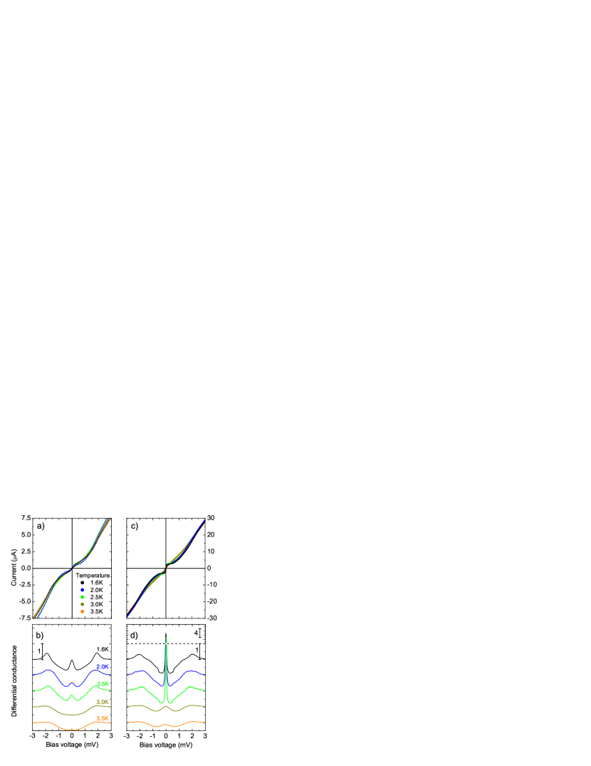
By fine tuning the piezo displacement stable metallic contacts can be produced with various sizes ranging from the single atom scale to contact diameters with a few microns. Here we discuss mostly the diffusive () point contacts, measurements in the ballistic limit are analyzed elsewhere Geresdi et al. (2008). The bias dependence of the differential conductance was investigated for several contacts of different radius. Typical sets of differential conductance curves and characteristics are shown in Fig. 1. The curves corresponding to a smaller junction [Fig. 1(a)-(b)] demonstrate a smooth growth of the zero bias peak resembling reflectionless tunneling phenomenon as the temperature is decreased. In contrast, for larger contact area [Fig. 1 (c) and (d)] we find a sharp increase of the peak amplitude instead of the smooth variation seen before. At the lowest temperatures the exhibits a huge central peak which is far beyond what is expected from the phenomenon of phase coherent multiple scattering; it rather resembles to Josephson critical current characteristic of superconductor–insulator–superconductor (SIS’) junctions Josephson (1962); Baselmans et al. (1999).
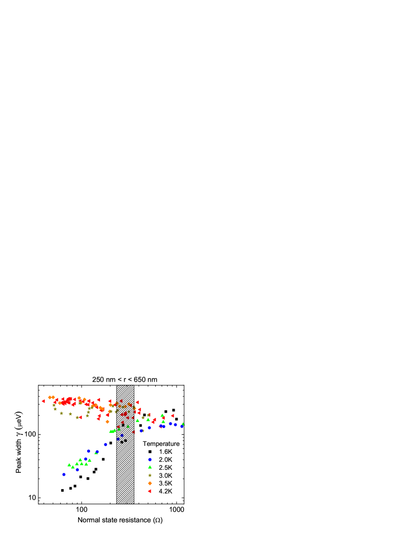
In order to get more insight into the above features we have measured a large number of contacts varying the contact size and temperature. The width of the measured zero-bias peak, is plotted against the contact normal state resistance in Fig. 2. For smaller contacts with normal state resistance larger than , no significant temperature dependence of is observed. For larger junctions, however, a clear transition is seen at K: at higher temperature takes a constant value of V, while at lower temperature it decreases with no apparent lower limit. The contact resistance at which this transition is observed (dashed region in Fig. 2) can be converted to contact size, revealing a critical contact radius of nm. It is worth noting here that the main source of error in the size determination is the uncertainty of the contact barrier strength, .
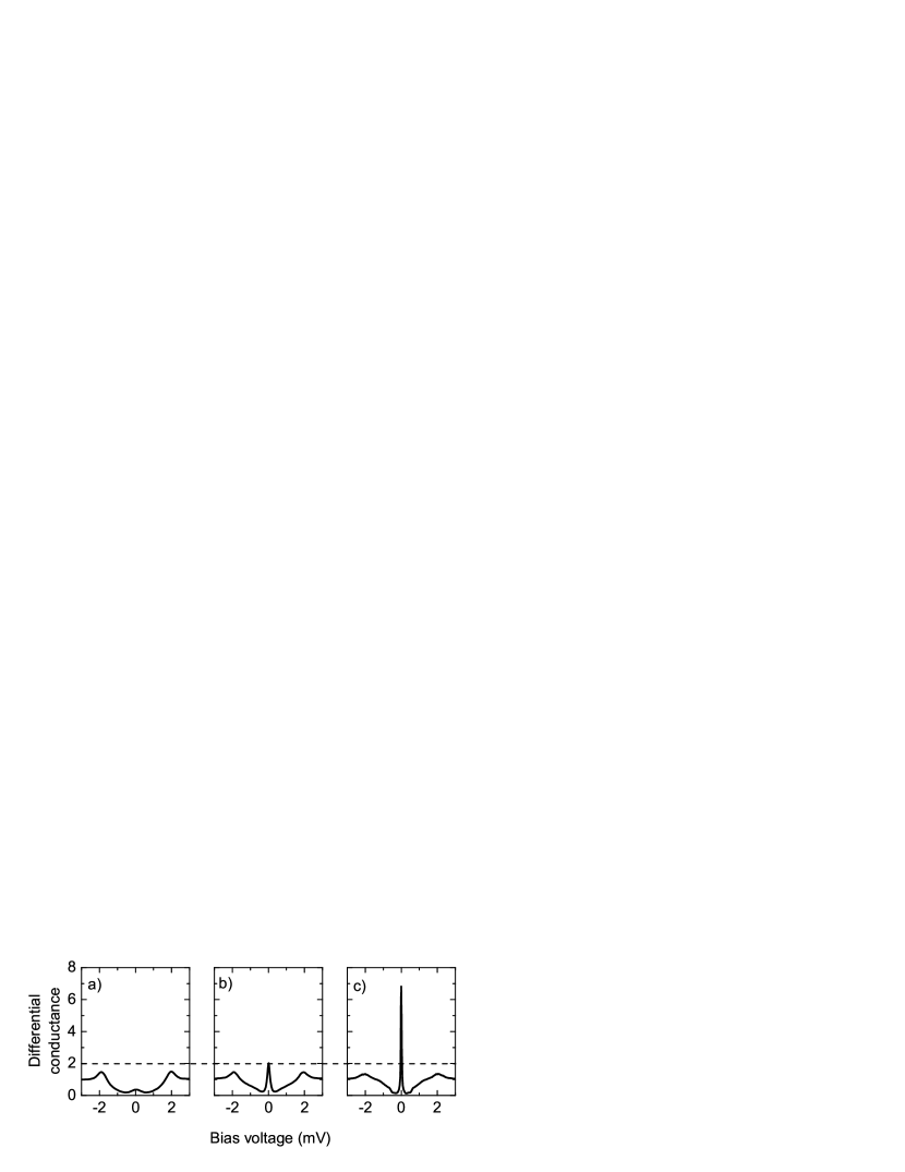
In Fig. 3 we demonstrate the evolution of the zero bias peak as the function of the contact size at the lowest measured temperature. The amplitude of the peak is not only increasing with increasing contact radius, but finally it highly exceeds the largest possible value for NS junctions, . This effect is studied for various contact resistances and temperatures in Fig. 4 by plotting the ratio of the zero bias and normal state conductance, and indicating the threshold value of with dashed line. Similarly to Fig. 2 a clear transition is observed: at low enough temperatures and large enough contact sizes the amplitude of the zero bias peak exceeds the limit for NS junctions. The critical temperature and contact radius coincide with those in Fig. 2.
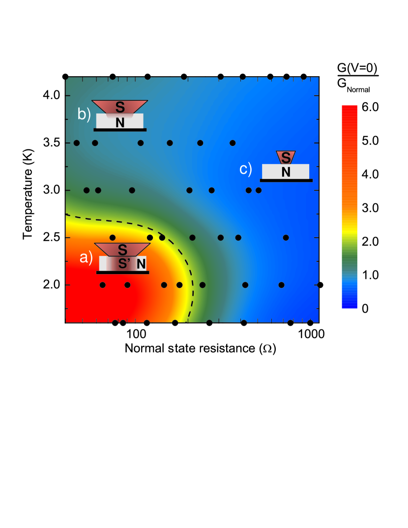
Discussing the experimental observations, first we emphasize that both the width and the amplitude of the zero bias peak indicate a rather sharp transition at a critical temperature and critical contact radius. For small contacts and high temperatures zero bias peaks with finite width and moderate amplitudes are observed, which are attributed to reflectionless tunneling phenomenon. However, for and the width of the peak abruptly decreases and its height grows highly above the theoretical upper limit for NS junctions. These features are characteristic of the formation of Josephson-current, i. e. supercurrent flowing through a barrier between two superconducting regions. The appearance of a peak narrower than is also a clear indication for the formation of proximity superconductivity in the normal side.
Next we analyze the geometrical constrictions present in the system. The size of the region where coherence is preserved is described by the phase coherence length,
| (1) |
where is the diffusion constant and is the possible energy difference between electron-hole pairs. At zero bias the dephasing is determined by the temperature . Substituting the critical temperature of K a phase coherence length of nm is obtained at the crossover temperature, which coincides with the thickness of the sample. This implies that proximity superconductivity builds up as the phase coherent scattering region reaches the bottom surface of the sample, and the density of the phase coherent electron-hole pairs is enhanced by surface backscattering. The critical contact radius, nm shows good agreement with the thickness of the sample, indicating that the critical coherent volume for the Cooper pair formation is reached when the radius of the contact becomes larger then the thickness of the normal region.
Based on these considerations the parameter space of our measurements can be divided into three characteristic regions. If the contact size is larger than the sample thickness, then most of the trajectories can bounce back and forth between the NS junction and the bottom of the sample. If this entire region is phase coherent, i. e. the trajectories do not loose phase information during several backscattering events, a proximity superconductivity builds up, and thus Josephson effect is observed [region (a) in Fig. 4]. In this region calculations based on a step-like function of the superconducting order parameter are not to be used anymore, and self-consistent methods Clerk et al. (2000); Taras-Semchuk and Altland (2001) are necessary to obtain proper transport properties. In contrast, only a small number of trajectories are scattered back coherently if the phase coherent region does not reach the bottom of the sample because the average pathway yields to a phase loss. In this case the conventional reflectionless tunneling is observed even for very large junctions [region (b)]. If the contact radius is smaller than the thickness of the sample, the normal region can be treated as an infinitely thick electrode, thus no crossover temperature is observed and a small correction is found [region (c)] similarly to region b). In these two latter cases, the width of the zero bias peak is mostly determined by the temperature, i. e. at phase coherence is destroyed by the bias voltage.
We note that in the proximity superconducting region (a) the low transparency NS interface is replaced by a Josephson junction, however a new mesoscopic normal -superconductor interface builds up between the proximity superconducting region, and the normal electrode. Here the transparency of the interface is large, but due to the small size of this interface and the 2D character of the sample a finite contact-resistance is still present. Based on simple estimations the spreading resistance of the thin film sample is expected to be , which is indeed observed in our measurements as a bottom limit of zero bias resistance. It is important to note that our findings were reproducible for different lateral positions on the sample. curves that were taken during pushing and retracting the tip were found to be identical.
The scheme of the proximity induced Josephson effect enhanced by the geometrical constrictions present in the system is in good agreement with our experimental findings. However, additional experiments can further verify the coherent nature of the huge zero bias peak, like detection of Shapiro steps under microwave irradiation or observation of Fraunhofer pattern in applied magnetic field. A systematic study of the layer thickness could also give insight into the details of the resonance condition.
In conclusion, we have studied the transport through variable size nanoscale NS junctions in a point contact geometry, by touching a thin metallic film with a superconducting tip. By increasing the contact size we have induced a clear transition from reflectionless tunneling phenomenon due to single particle mesoscopic interference effects to a Josephson supercurrent due to the condensation of Cooper pairs at the normal side. This transition is generated by forming a phase coherent resonator region between the junction and the opposite interface of the metallic film as both the diameter of the junction and the phase coherence length are enhanced above the thickness of the normal layer.
Acknowledgements.
The authors are grateful to J.K. Furdyna and T. Wojtowicz for supplying the (In,Be)Sb sample studied in this work. This work was supported by the New Hungary Development Plan under project ID: TÁMOP-4.2.1/B-09/1/KMR-2010-0002 and by the Hungarian Research Funds OTKA under grants No. 72916 and No. 76010. A. H. is a grantee of the Bolyai János scholarship.References
- Soulen et al. (1998) J. Soulen, R. J., J. M. Byers, M. S. Osofsky, B. Nadgorny, T. Ambrose, S. F. Cheng, P. R. Broussard, C. T. Tanaka, J. Nowak, J. S. Moodera, A. Barry, and J. M. Coey, Science, 282, 85 (1998).
- Cadden-Zimansky et al. (2009) P. Cadden-Zimansky, J. Wei, and V. Chandrasekhar, Nature Physics, 5, 393 (2009), ISSN 1745-2473.
- Hofstetter et al. (2009) L. Hofstetter, S. Csonka, J. Nygard, and C. Schonenberger, Nature, 461, 960 (2009), ISSN 0028-0836.
- Nakamura et al. (1999) Y. Nakamura, Y. A. Pashkin, and J. S. Tsai, Nature, 398, 786 (1999), ISSN 0028-0836.
- Makhlin et al. (1999) Y. Makhlin, G. Scohn, and A. Shnirman, Nature, 398, 305 (1999), ISSN 0028-0836.
- Mallet et al. (2009) F. Mallet, F. R. Ong, A. Palacios-Laloy, F. Nguyen, P. Bertet, D. Vion, and D. Esteve, Nature Physics, 5, 791 (2009), ISSN 1745-2473.
- Blonder et al. (1982) G. E. Blonder, M. Tinkham, and T. M. Klapwijk, Phys. Rev. B, 25, 4515 (1982).
- van Wees et al. (1992) B. J. van Wees, P. de Vries, P. Magnée, and T. M. Klapwijk, Phys. Rev. Lett., 69, 510 (1992).
- Schechter et al. (2001) M. Schechter, Y. Imry, and Y. Levinson, Phys. Rev. B, 64, 224513 (2001).
- Xiong et al. (1993) P. Xiong, G. Xiao, and R. B. Laibowitz, Phys. Rev. Lett., 71, 1907 (1993).
- Kastalsky et al. (1991) A. Kastalsky, A. W. Kleinsasser, L. H. Greene, R. Bhat, F. P. Milliken, and J. P. Harbison, Phys. Rev. Lett., 67, 3026 (1991).
- Magnée et al. (1994) P. H. C. Magnée, N. van der Post, P. H. M. Kooistra, B. J. van Wees, and T. M. Klapwijk, Phys. Rev. B, 50, 4594 (1994).
- Badolato et al. (2000) A. Badolato, F. Giazotto, M. Lazzarino, P. Pingue, F. Beltram, C. Lucheroni, and R. Fazio, Phys. Rev. B, 62, 9831 (2000).
- Dunford and Dhirani (2008) J. L. Dunford and A.-A. Dhirani, Phys. Rev. Lett., 100, 147202 (2008).
- Quirion et al. (2002) D. Quirion, C. Hoffmann, F. Lefloch, and M. Sanquer, Phys. Rev. B, 65, 100508 (2002).
- Geshkenbein and Sokol (1988) V. B. Geshkenbein and A. V. Sokol, Zh. Eksp. Teor. Phys., 94, 259 (1988).
- Han and Wolf (1987) S. Han and E. L. Wolf, Phys. Rev. B, 35, 4669 (1987).
- Han et al. (1990) S. Han, L. F. Cohen, and E. L. Wolf, Phys. Rev. B, 42, 8682 (1990).
- Agraït et al. (1992) N. Agraït, J. G. Rodrigo, and S. Vieira, Phys. Rev. B, 46, 5814 (1992).
- Wojtowicz et al. (2004) T. Wojtowicz, W. L. Lim, X. Liu, G. Cywinski, M. Kutrowski, L. V. Titova, K. Yee, M. Dobrowolska, J. K. Furdyna, K. M. Yu, W. Walukiewicz, G. B. Kim, M. Cheon, X. Chen, S. M. Wang, H. Luo, I. Vurgaftman, and J. R. Meyer, Physica E: Low-dimensional Systems and Nanostructures, 20, 325 (2004), ISSN 1386-9477, proceedings of the 11th International Conference on Narrow Gap Semiconductors.
- Csontos et al. (2005) M. Csontos, G. Mihaly, B. Janko, T. Wojtowicz, X. Liu, and J. K. Furdyna, Nat Mater, 4, 447 (2005), ISSN 1476-1122.
- Mihály et al. (2008) G. Mihály, M. Csontos, S. Bordács, I. Kézsmárki, T. Wojtowicz, X. Liu, B. Jankó, and J. K. Furdyna, Phys. Rev. Lett., 100, 107201 (2008).
- Geresdi et al. (2008) A. Geresdi, A. Halbritter, M. Csontos, S. Csonka, G. Mihály, T. Wojtowicz, X. Liu, B. Jankó, and J. K. Furdyna, Phys. Rev. B, 77, 233304 (2008).
- Wexler (1966) G. Wexler, Proceedings of the Physical Society, 89, 927 (1966).
- Woods et al. (2004) G. T. Woods, R. J. Soulen, I. Mazin, B. Nadgorny, M. S. Osofsky, J. Sanders, H. Srikanth, W. F. Egelhoff, and R. Datla, Phys. Rev. B, 70, 054416 (2004).
- Vurgaftman et al. (2001) I. Vurgaftman, J. R. Meyer, and L. R. Ram-Mohan, Journal of Applied Physics, 89, 5815 (2001).
- Josephson (1962) B. D. Josephson, Physics Letters, 1, 251 (1962), ISSN 0031-9163.
- Baselmans et al. (1999) J. J. A. Baselmans, A. F. Morpurgo, B. J. van Wees, and T. M. Klapwijk, Nature, 397, 43 (1999), ISSN 0028-0836.
- Clerk et al. (2000) A. A. Clerk, P. W. Brouwer, and V. Ambegaokar, Phys. Rev. B, 62, 10226 (2000).
- Taras-Semchuk and Altland (2001) D. Taras-Semchuk and A. Altland, Phys. Rev. B, 64, 014512 (2001).