Shape-dependent Depinning of a Domain Wall by a Magnetic Field and a Spin-Polarized Current
Abstract
The effect of sample shape on the depinning of the domain wall (DW) driven by an applied magnetic field or a spin-polarized current is studied theoretically. The shape effect resulting from the modulation of the sample width (geometric pinning) can essentially affects the DW depinning. We found a good agreement between the ratios of the critical values of the magnetic field and the spin-polarized current predicted by the theory and measured in the experiment.
pacs:
72.30.+q, 75.60.Ch, 75.70.Ak, 85.75.-dI Introduction
During the last years an immense interest in current-driven domain wall (DW) motion in thin magnetic films, nanotubes and point contacts has been initialized by possible applications in spintronic device technology (see, e. g. Marrows , Thomas and references therein). These devices are expected to be highly efficient, fast and consuming less energy. They possess such important features as non-volatility, portability and capability of simultaneous data storage and processing. A manipulation of magnetization by spin-polarized current predicted by Berger for non-uniform ferromagnets Berger and Slonczewski for multi-layered ferromagnetic structures Slonczewski1 has attracted the attention of physical community during last decade and gained further development in Li -Klein2 .
The problem of DW motion under another driving force, applied magnetic field, was addressed in late 70s in connection to possible application in memory storage devices (see, e. g. Malozemoff ). In pioneering work of Schryer and Walker Schryer it was shown the existence of an instability in the laminar movement of the DW. These early results can actually serve as a reference for the studies of spin-polarized current-driven DW motion. In particular, it is well established now that for DW driven by magnetic field (or spin-polarized current, or both) there exists a critical value of driving parameter(s) which corresponds to maximum velocity of the DW (Walker velocity Schryer ). Thus, the DW dynamics includes two distinct regimes, so-called subcritical (below the Walker breakdown) and supercritical (above the Walker breakdown) ones Marrows , Thiaville ). Below the Walker limit the overdamped transient response of the system to applied magnetic field follows by a steady state response, while above the Walker limit the DW dynamics is oscillatory with non-zero average velocity.
In case of field-driven DW motion the exact stationary wave solution in subcritical regime was obtained more than half-century ago by Walker Walker . Analytical results of Bourne Bourne reproduced a velocity profile in full range of magnetic field confirming numerical simulations of Slonczewski in supercritical regime Slonczewski2 .
Modern fabricated logic elements based on manipulation of the DWs are represented by a complex networks of nanowires, which can form three-dimensional memory storage structure, e. g., a racetrack device that comprises an array of magnetic nanowires arranged horizontally or vertically on a silicon chip Parkin . The spacing between consecutive DWs is controlled by pinning sites fabricated by patterning notches along the edges of the track or modulating the track’s size and material properties. Being a necessary component of the logic elements, the pinning sites define the bit length and provide the DWs stability against external perturbations, such as thermal fluctuations or stray magnetic fields from nearby racetracks. The variation of the nanowire geometry creates the pinning potential for the DW. The knowledge of the behavior of the DW in artificially created structural defects and constrictions is extremely important for producing reliable memory devices. In spite of a growing number of experimental studies which gain insight into the properties of the DWs pinned by artificial defects (see, e. g. Klein1 , Bogart -Ahn ), a detailed understanding of the role of the shape effects on the dynamics of the DW driven by magnetic field and (or) spin-polarized current is still lacking.
In this paper we study shape-dependent effects on the properties of DW confined in potential wells created by the defects in the bulk and by the variation of the sample shape (geometrical pinning). We analyze the difference in the depinning of the DW driven by applied magnetic field, from one side, and spin-polarized current, from another. We provide a plausible explanation of recent experimental data on manipulation of DW in constricted stripes of Klein1 .
II Geometry and Basic Equations
The DW displacement under driving magnetic field and spin-polarized current can be adequately described by Landau-Lifschitz-Gilbert (LLG) equations complemented by a spin-transfer torque, :
| (1) |
where is the gyromagnetic ratio, is the dissipation parameter, is effective magnetic field, is free energy density of the ferromagnet, and is a unit vector in the direction of the magnetization ( is the saturation magnetization).
Despite different approaches in calculation of the spin-transfer torque , there is a consensus about the existence of adiabatic and non-adiabatic terms (or -term Tatara1 ) that contribute to the spin-transfer torque
| (2) |
where , ( is Bohr magneton, is the elementary charge, is the current , is a value of the current, is a cross-section area of the sample and is the spin polarization), is unit vector in the direction of the current. Parameter is a ratio between the values of non-adiabatic and adiabatic torques.
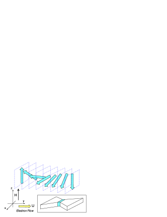
Let us consider the DW of Bloch type in a constricted plate-like sample with variable size along direction and constant dimensions and along and axis as shown in Fig. 1. The function describes the change of the sample shape. In absence of constriction and . The DW width, , is much less than the width of the plate, , i.e. . The surface of the sample is parallel to the -plane, and the domain wall, being parallel to the -plane, separates two domains with magnetization along the or direction and is located initially in the constriction at 0.
The free energy functional of the ferromagnet is where the free energy density is defined by
| (3) |
Here, the first and second terms in square brackets describe the magnetic crystallographic anisotropy, the third term is the exchange energy and the last term is the Zeeman energy in an external magnetic field . In Eq. (3) 0 is the parameter of the easy-axis crystallographic anisotropy, the ratio 0 determines a joint effect of orthorhombic anisotropy and the magnetostatic energy, and is a half-width of the DW at rest, which characterizes the stiffness of the spin system. The choice of the sign 0 implies alignment of the magnetization in the -plane. Thus, in the absence of the driving force the formation of DW of Bloch type with the rotation of the magnetization in -plane is energetically more favorable.
The magnetization can be expressed in polar coordinates, . In the absence of driving forces (0) the ground state of the system is defined by minimization of the free energy with respect to azimuthal, , and polar, , angles, i.e., and . This yields the well-known structure of Bloch DW located at the center of the sample constriction (0): and .
The standard approach in statics and dynamics of the DW is to use the Slonczewski equations for two canonically conjugated variables, the coordinate of the center of the DW , and azimuthal angle (see, e. g. Malozemoff ), which are independent of the coordinate . For a sample with variable cross-section area ( is the area of the cross-section at 0, and is a shape function dependent on the geometry of the sample) these equations are:
| (4) |
where , is the effective DW width, and is the surface energy of the DW determined by the integral across the whole DW width:
| (5) |
The goal of the present work is not investigation of the DW motion but determination of the depinning threshold, when such motion becomes possible. Therefore, one may ignore the time dependence of the variables. The second term in the spin torque (nonadiabatic torque), Eq. (2), is most relevant for depinning. This term is related to the momentum transfer between the polarized current and the DW. The adiabatic torque [the first term in Eq. (2)] causes the rotation of the DW plane around axis relative to it equilibrium position (plane), but does not affect the DW depinning directly.
III Depinning of Domain Walls
Usually, the pinning (coercivity) force on a DW originates from randomly located defects, which create potential wells for the DW in the sample bulk. However, key features of the bulk pinning phenomenon can be investigated using a simpler model of a DW in a periodic potential. The latter enters the DW surface energy, i.e., with , where is a periodic function with a period 2. Within the period () this function can be approximated by a parabolic function . In addition to the pinning on the defects, there is another type of pinning (geometrical pinning) related to the change of the sample shape. Eventually neglecting the structure of the DW, i.e., assuming that , we obtain
| (6) |
where is a magnetic field corresponding to the easy-axis magnetic crystallographic anisotropy of a sample. According to Eq. (6), the modulation of the sample width gives rise to an effective geometrical pinning of the DW. It follows from Eqs. (6) that DW can be depinned by action of magnetic field, , or the nonadiabatic contribution of the spin-polarized current, .
In the following, we consider two particular cases, , and , .
III.1 Depinning by applied magnetic field: ,
In case of 0 and , it follows from Eqs. (6), that , , and the depinning of the DW by magnetic field is not affected by the presence of the orthorhombic anisotropy. Thus, instead of the first equation in (6) we have
| (7) |
Equation (7) manifests the absence of a total force experienced by DW. The driving force from the magnetic field (the term ) and the bulk pinning force confining the DW in a potential well (the term ) are proportional to the total DW area, , while the force experienced by the DW in a shape-dependent pinning potential is determined by the derivative of the shape function [the last term in Eq. (7)].
For simple shape potential, which can be expanded in series on DW displacement , the function reaches a maximum at some value of the parameter . Thus, it is insightful to characterize the geometric pinning potential, which is responsible for the shape effect, by the strength of the potential and the characteristic distance , which are analogous to the parameters and of the pinning potential due to the defects. The value of the critical magnetic field is defined by
| (8) |
while is obtained from the condition of a potential extremum 0.
Thus, the presence of a constriction results in the change of the DW area and appearance of the geometrical pinning, which is independent of the distribution of defects. In absence of pinning on defects (), the increase in the applied magnetic field below the critical field () causes the DW displacement (which is not a linear function of a magnetic field in general) until its depinning at .
With use of and both terms that contribute to the DW pinning [see Eq. (7)] can be rewritten in a similar way:
| (9) |
where is a step-function, and the function is defined according to
| (10) |
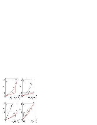
Equation (9) defines a function and can be solved for given geometry of the constriction. The results of numerical calculation of the function in the particular case of a parabolic potential created by the constriction when are shown in Fig. 2 and reveal the general features of the DW depinning by the applied magnetic field . Figure 2 illustrates the possibility of four different scenarios of DW depinning dependent on the relation between and , from one side, and and , from another. The analysis shows that these scenarios can be classified according to the values of two critical parameters, namely, the depinning magnetic field and critical value of the DW displacement . The value of and are defined according to
| (11) |
and
| (12) |
where we assume that the maximum width of the constriction along -axis exceeds the critical distance . For () the pinning potential cannot stop motion of the DW.
III.2 Depinning by a spin-polarized current: ,
In the case of , , instead of Eqs. (6) we have another pair of equations:
| (13) | |||
| (14) |
Equation (13) manifests the balance of forces on the DW: the forces from the spin-polarized current () and the geometrical pinning (), and the bulk pinning force (). Equation (14) defines the function :
| (15) |
where . Substituting Eq. (15) into Eq. (13) one can calculate the function . For the sake of simplicity we neglect the change of the DW width assuming that , which is true if 1 ( 1). In this case Eq. (13) can be rewritten in a following way:
| (16) |
It follows from Eq. (16), that in an unconstricted sample (0) a DW can be depinned and participate in a steady-state motion when the the current exceeds the critical value defined by the equation .
The condition for DW geometric depinning by the current is more severe than by the magnetic field. This because the pressure on the DW from the constant magnetic field (the force per unit area of the DW) does not depend on the DW area growing with the DW displacement, whereas the pressure from the constant current is determined by the current density, which is inversely proportional to the DW area. According to Eq. (16) at , the critical value of a current is determined by the threshold above which the DW can overcome the geometrical pinning. For a parabolic shape function , the function is unbound, and DW depinning from the geometric pinning potential is impossible. Let us consider the DW behavior in this case.
We assume that a single DW is initially located in the constricted area ( 0). The increase of the current density above its critical value at a given position of the DW results in the drift of the DW from the constriction into expansion part of the sample. Such a drift is accompanied by the increase in the DW area followed by the decrease of the current (the current does not depend on the location of the DW) below its critical value. As a result, the DW will be eventually pinned in a new position by an array of the nearest defects. The further increase in the current results in increase in a driving force and a displacement of the DW into a new position where the driving force is balanced by the increase in the pinning force. At this new position the DW is stuck again till the next increase of the current. Actually, in the presence of bulk pinning centers the displacement of the DW under spin-polarized current is characterized by a step-by-step drift over an array of bulk defects.
Equation (16) can be solved numerically for given functions and . The results of numerical calculation of the function for a parabolic shape function are present in Fig. 3 which illustrates the absence of the critical point on the curve ( when ), contrary to the case of depinning of a DW driven by a magnetic field (see Fig. 2).
III.3 Domain wall in a constricted sample of and comparison with experiment
The developed theory can be exploited to understand the data on depinning of the DW from double -shape constriction in submicroscopic patterns of Klein1 . is a metallic perovskite with orthorhombic structure (5.53, 5.57, 7.82 ) and an itinerant ferromagnet with Curie temperature of and a saturated magnetization of per ruthenium. It shows so-called bad metal behavior at high temperatures, but is a Fermi liquid at low temperatures. exhibits a positive Seebeck coefficient in the wide range of the temperature from 0 K till 1000 K Klein , Maekawa , manifesting the hole-like character of the charge carriers. The samples are high-quality epitaxial thin films of grown by reactive electron beam coevaporation on slightly miscut ( substrates with the and axes in the film plane. These films exhibit a large uniaxial magnetocrystalline anisotropy (anisotropy field T at 0 K) with the easy axis tilted out of the film () and with an in-plane projection along . Consequently, the domain magnetization is out of film plane, the Bloch DWs are parallel to axis and the orthorhombic anisotropy (including the magnetostatic energy related to the shape anisotropy of the sample) contributes to the structure of the DW. Due to the large uniaxial magnetic anisotropy the DWs are relatively narrow with temperature independent width of .
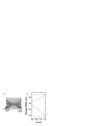
The experimental setup is shown in Fig. 4 (a). The measurements on the displacement of the DW driven by magnetic field and spin-polarized current were performed on a high-quality thick film of with the resistivity ratio of ( at ). The DW initially located at the constriction (see, Fig. 4 (a)) was unpinned under the action of a magnetic field or a spin-polarized current and moved in the positive direction of -axis (parallel to ) towards the pair of leads EF. The magnetic state of the sample in the region of contacts EF was monitored by measuring of extraordinary Hall effect (EHE) proportional to the average component of magnetization perpendicular to the film plane (-plane). The final location of the DW at the leads EF was deduced by the change of the sign of EHE followed by the change of the magnetic state at EF. The experiment shows that the DW displacement into a final position at the leads EF is achieved only with a value of the magnetic field (current density) above a certain threshold for the magnetic field or the current.
The shape of the sample [see Fig. 4 (b)] can be approximated by a function
| (17) |
where =1.138 m, =2.6 m, =0.561 m, and =0.52 m. The results of numerical calculation show that a function has a maximum at =0.44 m with =1.1675 m-1. The assumption , which is true assuming that 1.5 nm, leaves two possibilities for the critical value of magnetic field [see Eq. (11)]:
| (18) |
where we use for . The choice of in Eq. (18) depends on the critical value of magnetic field corresponding to the geometrical pinning given by Eq. (8). Using the values of 10 T and 1.5 nm Klein1 , we obtain 160 Oe, which is less than the highest value of the depinning field 500 Oe measured at the temperature 40 K Klein1 . Therefore, we conclude that the critical magnetic field measured in Ref. Klein1, is dominated by the contribution of bulk pinning on defects, i.e., , in accordance with the conclusions of Klein1 . Evaluating the critical field (18), we have neglected the small contribution of , which is on the order of several Oe. It follows from Eq. (12) that the critical value of the DW displacement is 1.5 nm 0.44 m, therefore the scenario illustrated in Fig. 2 (b) is realized. After depinning when and 1.5 nm the DW moves freely (see Ref. Tatara2, ) till it reaches the leads EF (Fig. 4 (a)).
In case of current driven DW motion the measured value of a spin-polarized current corresponds to the arriving of the DW at the leads EF (see Fig. 4 (a)). Both contributions to the DW pinning resulting from the distribution of the defects and the change of the sample shape can be evaluated from the data Klein1 by use of Eq. (16). To calculate the value of the current predicted by the theory we replace in Eq. (16) by its maximum value: 1,
| (19) |
Furthermore, we assume that the DW moves at the distance 1.5 m till it is registered by observation of the change of the sign of extraordinary Hall effect at the leads EF (see, Fig. 4). With use of 10 T, 1.5 nm and the measured value of the depinning field 571 Oe at 40 K Klein1 one can show that 411 Oe and 2250 Oe which gives a relative contribution of the geometrical pinning 20 . The measurement of the corresponding current density allows to evaluate the parameter of the non-adiabaticity . For , the current density translates into the velocity according to [m/s]= 3.64 10[A/m]. Substituting the measured value of the current density 5.8 1010 A/m2 into Eq. (19) Klein1 and using the value of spin polarization 0.5 (see Ref. Nadgorny, ) we obtain 6. Being in accord with the conclusions of the high efficiency of monitoring of the DW by spin-polarized current in Klein1 , such large value of cannot be explained by the contribution of the spin-relaxation process, which gives the value of 1 (see Refs. Thiaville, , Zhang, ), but can be understood due to the dominant role of the reflection of the charge carriers from thin DWs in the framework of the theory developed in Ref. Tatara1, .
Since bulk pinning on defects varies from a sample to sample, it is unpractical to look for quantitative comparison of the theory and the experiment in the case of predominantly bulk pinning. However, if there are data for the critical magnetic field and the critical current for the same sample, one may easily find from the theory their ratio and compare it with the experimental values. As it was shown by Tatara and Kohno Tatara1 the dynamics of the abrupt DW in ideal plate-parallel sample is dominated by the momentum transfer from the charge current to the DW via reflection of charge carriers from the DW. Since this momentum transfer determines also the DW contribution to the resistance, in accordance with Ref. Tatara1, the parameter can be found from the relation
| (20) |
where is a total charge carrier density and is the DW contribution to the resistance. Substituting Eq. (20) into Eq. (16), we arrive at the equation that defines the value of the current density as a function of the displacement of the DW in the presence of bulk and geometric pinning. As was pointed out in Sec. III.2, complete depinning of the DW from the potential produced by growing cross-section of the sample is impossible.However, one may introduce the critical current density (determined at the constriction), at which the DW reaches the position where the DW is detected (the leads EF in Fig. 4). Then
| (21) |
where is the distance between the sample constriction and the place of DW detection, and
| (22) |
is the critical current density of depinning for the DW in an unconstricted sample.
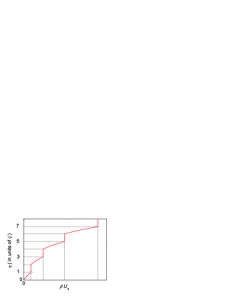
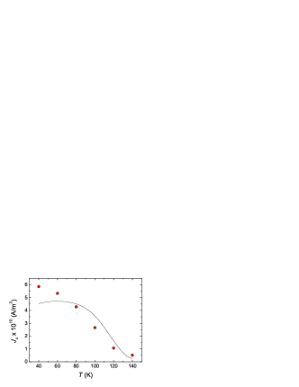
The temperature dependent saturation magnetization and the DW resistance were measured in Refs. Klein3, and Klein1, respectively. According to Ref. Klein1, the carrier density is about 1.6 1028 [1/m3]. This offers an opportunity to compare the developed theory with the data Klein1 . Calculating the critical current density with help of Eq. (21), we assume that the relative contribution of the geometric pinning [the term in Eq. (21)] is temperature independent and equals to the value of 20 calculated at 40 K. Then Eq. (21) yields 5. Figure 5 shows the experimentally determined critical current density (cicles) together with the prediction of the theory using the experimentally found critical magnetic fields and taking into account the shape dependent effect (geometric pinning). The figure illustrates a satisfactory agreement between the experiment and the theory.
It is important to note that the sign of the ratio between the current and the DW displacement depends on the sign of charge carriers. The relative sign of the current and the displacement in the experiment gives evidence that charge carriers are holes. This agrees with the experiment on the Seebeck effect Klein .
IV Conclusions
We investigated pinning of a domain wall by potentials produced by bulk defects and the sample shape. The process of depinning by an external magnetic field and by a spin-polarized current was analyzed. The shape-dependent pinning potential (geometric pinning) can essentially affect the process of depinning and may even make complete depinning by the spin-polarized current impossible. Though the absolute values of the critical magnetic fields and the critical currents, at which depinning occurs, are sample dependent and difficult for theoretical prediction, their ratio must be sample independent Tatara1 and allows reliable comparison of the theory and the experiment. We performed this comparison and found a satisfactory agreement.
Aknowledgments
We appreciate the useful discussions with L. Klein. This work has been supported by the grant of the Israel Academy of Sciences and Humanities and grand of the Israel Scientific Foundation (Grand No. 499/07).
References
- (1) C. H. Marrows, Adv. in Phys. 54 585 (2005).
- (2) L. Thomas, M. Hayashi, X. Jiang, R. Moriya, C. Rettner, and S. S. P. Parkin, Nature 443, 197 (2006).
- (3) L. Berger, Phys. Rev. B 54 9353 (1996); L. Berger, Phys. Rev. B 73 014407 (2006).
- (4) J. C. Slonczewski, J. Magn. Magn. Mater. 159 L1 (1996).
- (5) Z. Li and S. Zhang, Phys. Rev. B 70 024417 (2004).
- (6) G. Tatara and H. Kohno, Phys. Rev. Lett. 92 086601 (2004); G. Tatara, H. Kohno, and J. Shibata, J. Phys. Soc. J. 77 031003 (2008).
- (7) A. Thiaville, Y. Nakatani, J. Miltat, and N. Vernier, J. Appl. Phys. 95 7049 (2004); A. Thiaville, Y. Nakatani, J. Miltat, and Y. Suzuki, Europhys. Lett. 69 990 (2005).
- (8) S. Zhang and Z. Li, Phys. Rev. Lett. 93 127204 (2004).
- (9) S. E. Barnes and S. Maekawa, Phys. Rev. Lett. 95 107204 (2005).
- (10) O. Boulle, J. Kimling, P. Warnicke, M. Klui, U. Rdiger, G. Malinowski, H. J. M. Swagten, B. Koopmans, C. Ulysse, and G. Faini, Phys. Rev. Lett. 101 216601 (2008).
- (11) M. Feigenson, J. W. Reiner, and L. Klein, Phys. Rev. Lett. 98 247204 (2007).
- (12) M. Feigenson, J. W. Reiner, and L. Klein, J. Appl. Phys. 103 07E741 (2008).
- (13) A. P. Malozemoff and J. C. Slonczewski, Magnetic Domain Walls in Bubble Materials (Academic, New York, 1976).
- (14) N. L. Schryer and L. R. Walker, J. Appl. Phys. 45 5406 (1974).
- (15) L. R. Walker (unpublished). The calculation is reproduced by J. F. Dillon, Jr. in Treatise on Magnetism, edited by G. T. Rado and H. Suhl (Academic, New York, 1963), Vol. III, p.450.
- (16) H. C. Bourne and D. S. Bartran, IEEE Trans. on Magn. MAG-10 1081 (1974).
- (17) J. C. Slonczewski, J. Appl. Phys. 44 11759 (1973).
- (18) S. S. P. Parkin, M. Hayashi, and L. Thomas, Science 320 190 (2008).
- (19) L. K. Bogart, D. Atkinson, K. O Shea, D. McGrouther, and S. McVitie, Phys. Rev. B 79 054414 (2009).
- (20) D. Petit, A.-V. Jausovec, H. T. Zeng, E. Lewis, L. O’Brien, D. Read, and R. P. Cowburn, Phys. Rev. B 79 214405 (2009).
- (21) A. Kunz and S. C. Reiff, Appl. Phys. Lett. 94 192504 (2009).
- (22) S.-M. Moon, K.-W. Moon, D.-H. Kim, and S.-B. Choe, Appl. Phys. Lett. 95 152506 (2009).
- (23) Y. Klein, S. Hebrt, A. Maignan, S. Kolesnik, T. Maxwell, and B. Dabrowski, Phys. Rev. B 73 052412 (2006).
- (24) T. Maekawa, K. Kurosaki, H. Muta, M. Uno, and S. Yamanaka, Journ. Alloys and Comp. 387 56 (2005).
- (25) G. Tatara, H. Kohnoc, and J. Shibata, Physics Reports 468 213 (2008).
- (26) B. Nadgorny, M. S. Osofsky, D. J. Singh, G. T. Woods, R. J. Soulen Jr., M. K. Lee, S. D. Bu, and C. B. Eom, Appl. Phys. Lett. 82 427 (2003).
- (27) L. Klein, J. S. Dodge, T. H. Geballe, A. Kapitulnik, A. F. Marshall, L. Antognazza and K. Char, Appl. Phys. Lett. 66 2427 (1995).