Optomechanics in an ultrahigh- slotted 2D photonic crystal cavity
Abstract
Optical guided wave dielectric structures with nanoscale slots are known to provide strong electric field enhancements in the slotted region, enabling strong light-matter interactions. Here we demonstrate an ultrahigh- slotted 2D photonic crystal cavity for the purpose of obtaining strong interaction between the internal light field and the mechanical motion of the slotted structure. The experimentally measured optical quality factor is for a cavity with a simulated effective optical modal volume of . Optical transduction of the thermal Brownian motion of the fundamental in-plane mechanical resonance of the slotted structure ( MHz) is performed, from which an optomechanical coupling of GHz/nm is inferred for an effective motional mass of pg. Dynamical back-action of the optical field on the mechanical motion, resulting in both cooling and amplication of the mechanical motion, is also demonstrated.
pacs:
The strength of the interaction between light and matter, which is fundamental to many applications in nonlinear and quantum optics, depends on the ability to create a large optical energy density, either through increased photon number or photon localization. This may be achieved by creating optical cavities with large quality factors and simultaneously small modal volumes . The mode volume in particular can be decreased through the introduction of slots, increasing the electric field intensity in low-index regions of the device. As such, slotted photonic crystal cavities Robinson et al. (2005) and waveguides Riboli et al. (2007) have been previously proposed and applied to create highly sensitive detectors of motion Eichenfield et al. (2009a); Lin et al. (2009) and molecules Di Falco et al. (2009). They have also more recently been studied in the context of Purcell enhancement of spontaneous emission from embedded quantum dots Gao et al. (2010).
In the canonical optomechanical system, consisting of a Fabry-Perot resonator with an oscillating end-mirror Kippenberg and Vahala (2008), the radiation pressure force per cavity photon is given by , where is the cavity resonance frequency, is the position of the end mirror, and is approximately equal to the physical length of the cavity. The optomechanical coupling length in such “diffraction-limited” cavities is limited approximately by the wavelength of light, . Large optomechanical coupling, approaching , has recently been realized in several different guided wave optical cavity geometries utilizing nanoscale slots Eichenfield et al. (2009a); Lin et al. (2009); Roh et al. (2010). In this work we design, fabricate, and measure the optomechanical properties of a slotted two-dimensional (2D) photonic crystal cavity formed in a Silicon membrane. Due to the strong optical confinement provided by a sub- nm slot and a two-dimensional photonic bandgap, this cavity structure is demonstrated to have an optical quality factor , a sub-wavelength , and a deep sub-cubic-wavelength optical mode volume.
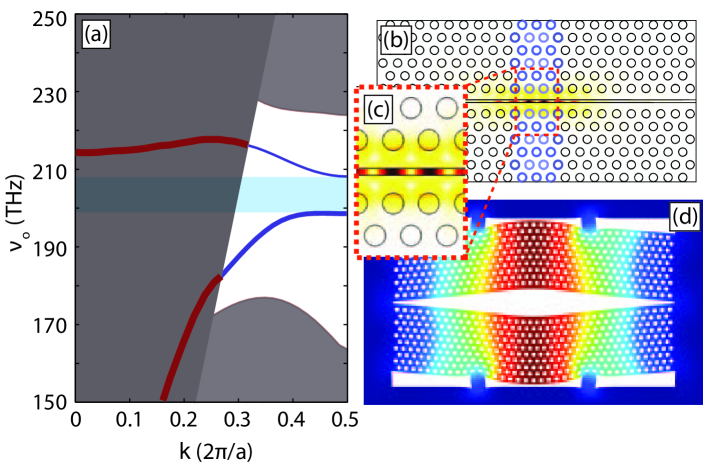
A common approach to forming photonic crystal optical circuits is to etch a pattern of holes into a thin dielectric film such as the top Silicon device layer in a Silicon-On-Insulator (SOI) microchip. An effective means of forming resonant cavities in such quasi-2D slab photonic crystal structures is to weakly modulate the properties of a line-defect waveguide Johnson et al. (2000); Chutinan and Noda (2000); Song et al. (2005). Applying this same design principle to slotted photonic crystal waveguides Di Falco et al. (2008), optical cavities with have been experimentally demonstrated Gao et al. (2010); Di Falco et al. (2009). A major source of optical loss in real fabricated structures is light scattering out of the plane of the slab. One class of optical states which play an important role in determining scattering loss are the resonant leaky modes of the slab. These optical resonances are localized to the slab and yet have wavevector components which radiate energy into the surrounding cladding. To reduce the effects of these modes it is preferable to engineer a structure where the photonic crystal waveguide has no leaky mode bands crossing the localized cavity mode frequency. For the popular W1 waveguide Johnson et al. (2000); Chutinan and Noda (2000) with a slot added in the waveguide center, we have found that the choice of the slot width is crucial to avoiding coupling to leaky resonances. Figure 1(a) shows the bandstructure of a slotted W1 waveguide with a hole radius nm, slot size nm, thickness nm, and nominal lattice constant of nm. A large bandgap for both guided and leaky modes (a “quasi-bandgap”) is clearly present in this structure for the TE-like (even vector parity) modes of the waveguide. On the otherhand, for slot widths the quasi-bandgap of the waveguide closes due to the presence of leaky resonant bands.
In order to form a localized cavity resonance, we begin with the slotted cavity waveguide structure of Figure 1(a). A localized resonance is created from the lower frequency waveguide band by reducing smoothly the local lattice constant from a nominal value of to a value of in the center of the cavity. Three-dimensional finite-element-method (FEM) simulations of the optical and mechanical properties of the resulting cavity structure were performed. The simulated electric field intensity of the fundamental confined optical mode is shown in Fig. 1(b). This mode has a resonance wavelength of nm, a theoretical radiation-limited and an effective optical mode volume of .
To allow for mechanical motion of the structure, three rectangular holes of dimensions are cut on each side of cavity device as shown in Fig. 1(d). FEM simulations show that this allows for a fundamental in-plane mechanical mode of motion with frequency and an effective motional mass of . The optomechanical coupling between the localized optical and mechanical modes is computed using a variation Johnson et al. (2002) of the Hellman-Feynman perturbation theory adopted for optomechanical systems Eichenfield et al. (2009b), yielding a sub-wavelength optomechanical coupling length of . This optomechanical coupling length corresponds to an optical frequency shift per nanometer of mechanical displacement of , or in the quantum realm a phonon-photon coupling rate of .
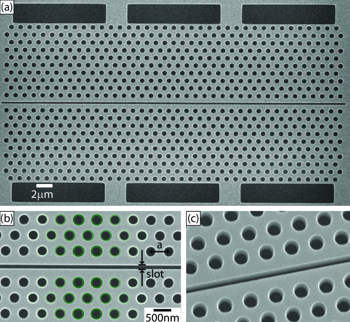
Slotted cavities with the dimensions stated above are fabricated using a Silicon-On-Insulator wafer from SOITEC (- cm, device layer thickness nm, buried-oxide layer thickness m). The cavity geometry is defined by electron beam lithography followed by reactive-ion etching to transfer the pattern through the silicon device layer. The cavities are undercut using solution to remove the buried oxide layer, and cleaned using a piranha/HF cycle Borselli et al. (2006). A scanning electron microscope (SEM) micrograph of a final device is shown in Fig.2(a). Fig. 2(b) and Fig. 2(c) show the local waveguide defect and slotted region of the cavity, respectively.
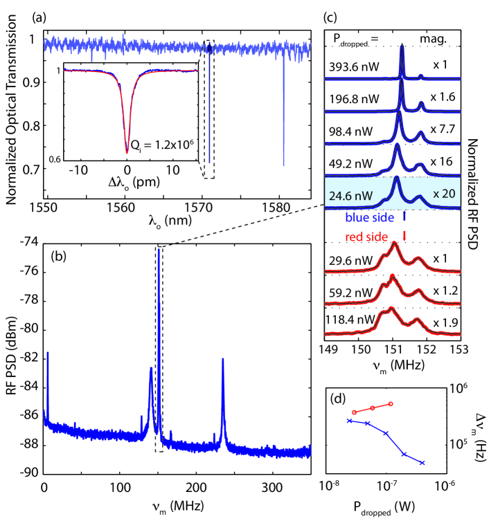
The resulting devices are characterized optically using a swept-wavelength external-cavity laser (, ), connected to a dimpled fiber-taper probe Michael et al. (2007). A broadband cavity transmission spectrum is shown in Fig. 3(a), with the first- and second-order optical cavity modes separated by roughly by , in agreement with simulations. For the first-order mode, optical on the order of is measured consistently in these devices. A narrowband optical transmission spectrum (calibrated using a fiber Mach-Zender interferometer) for one such device is shown in the inset of Fig. 3(a), with a measured instrinsic optical .
The mechanical properties of the slotted photonic crystal cavity are measured by driving the system with the laser frequency locked to a detuning of a half-linewidth (blue or red) from the cavity resonance. The transmitted cavity laser light is sent through an erbium doped fiber amplifier and then onto a high-speed photodetector. The photodetected signal is sent to an oscilloscope ( GHz bandwidth) where the electronic power spectral density (PSD) is computed. An example of the measured RF-spectrum from a typical slotted cavity device is shown in Fig. 3(b). The fundamental in-plane mode, corresponding to the largest peak in the spectrum, is found to occur at a frequency of , very close to the simulated value of MHz. RF spectra for various dropped optical powers into the cavity are shown in Fig. 3(c). The corresponding mechanical linewidth is plotted in Fig. 3(d). The effects of the retarded component of the dynamical back-action Kippenberg and Vahala (2008) of the light field on the mechanical resonance are clear in both plots, with red (blue) detuning resulting in a reduction (amplification) in the mechanical resonance peak height and a broadening (narrowing) of the mechanical linewidth. One curious aspect of the measured mechanical spectra, however, are the two smaller side peaks on either side of the main resonance line. These side peaks are thought to arise due to a mixing of the in-plane mode with nearby flexural (out-of-plane) resonances of the slab. FEM simulations indicate the presence of several flexural modes located within a few MHz of the fundamental in-plane mode, which can mix with in-plane motion through a breaking of the vertical symmetry of the slab. As an example, SEM images show that the membranes are subject to weak stress-induced bowing, which can lead to this effect.
The optomechanical coupling of the fundamental in-plane mechanical resonance can be estimated using two different methods. The first method involves calibration of the optical powers and electronic detection system, and uses the fact that the transduced thermal Brownian motion of the mechanical resonator is proportional to Eichenfield et al. (2009c). The second method compares the ratio of the RF power in the first and second harmonic of the mechanical frequency. This method is independent of the absolute optical power and detection efficiency, and relies only on accurate knowledge of the optical linewidth. Both of these methods were found to yield an experimental optomechanical coupling of ( m) for the fundamental in-plane mechanical resonance (assuming pg), roughly a factor of times smaller than the FEM-estimated value. As alluded to above, this discrepancy is thought to result from mixing of in-plane motion with optomechanically “dark” (i.e., no coupling to first-order in motional amplitude) flexural modes of the patterned slab.
In summary, the slotted photonic crystal cavity described here reduces optical scattering loss through the avoidance of resonant leaky modes of the structure while simultaneously allowing for large electric field enhancement in the cavity slot region. The demonstrated optical loss rate of the cavity is MHz, which in conjunction with the high mechanical frequency ( MHz) of the fundamental in-plane mechanical resonance, puts this system in the resolved sideband limit of cavity optomechanics (). The resolved sideband limit is important for a variety of applications, including optical cooling of the mechanical motion to the quantum mechanical ground-state Marquardt et al. (2007); Wilson-Rae et al. (2007). The optomechanical coupling is estimated to be GHz/nm for the slotted cavity, due largely to the electric field enhancement in the slot and corresponding to one of the largest values measured to date Van Thourhout and Roels (2010). The estimated ratio for the measured devices is , indicating that these slotted cavities may also find use in other applications such as Silicon-based cavity-QED Gao et al. (2010) and sensing Di Falco et al. (2009).
This work was supported by the DARPA/MTO ORCHID program through a grant from AFOSR, and the Kavli Nanoscience Institute at Caltech. ASN gratefully acknowledges support from NSERC.
References
- Robinson et al. (2005) J. T. Robinson, C. Manolatou, L. Chen, and M. Lipson, Phys. Rev. Lett. 95, 143901– (2005).
- Riboli et al. (2007) F. Riboli, P. Bettotti, and L. Pavesi, Opt. Express 15, 11769 (2007).
- Eichenfield et al. (2009a) M. Eichenfield, R. Camacho, J. Chan, K. J. Vahala, and O. Painter, Nature 459, 550 (2009a).
- Lin et al. (2009) Q. Lin, J. Rosenberg, X. Jiang, K. J. Vahala, and O. Painter, Phys. Rev. Lett. 103, 103601 (2009).
- Di Falco et al. (2009) A. Di Falco, L. O’Faolain, and T. F. Krauss, Appl. Phys. Lett. 94, 063503 (2009).
- Gao et al. (2010) J. Gao, J. F. McMillan, M.-C. Wu, J. Zheng, S. Assefa, and C. W. Wong, Appl. Phys. Lett. 96, 051123 (2010).
- Roh et al. (2010) Y.-G. Roh, T. Tanabe, A. Shinya, H. Taniyama, E. Kuramochi, S. Matsuo, T. Sato, and M. Notomi, Phys. Rev. B 81, 121101 (2010).
- Kippenberg and Vahala (2008) T. J. Kippenberg and K. J. Vahala, Science 321, 1172 (2008).
- Johnson et al. (2000) S. G. Johnson, P. R. Villeneuve, S. Fan, and J. D. Joannopoulos, Phys. Rev. B 62, 8212 (2000).
- Chutinan and Noda (2000) A. Chutinan and S. Noda, Phys. Rev. B 82, 4488 (2000).
- Song et al. (2005) B.-S. Song, S. Noda, T. Asano, and Y. Akahane, Nat Mater 4, 207 (2005).
- Di Falco et al. (2008) A. Di Falco, L. O’Faolain, and T. F. Krauss, Appl. Phys. Lett. 92, 083501 (2008).
- Johnson et al. (2002) S. G. Johnson, M. Ibanescu, M. A. Skorobogatiy, O. Weisberg, J. D. Joannopoulos, and Y. Fink, Phys. Rev. E 65, 066611 (2002).
- Eichenfield et al. (2009b) M. Eichenfield, J. Chan, A. H. Safavi-Naeini, K. J. Vahala, and O. Painter, Opt. Express 17, 20078 (2009b).
- Borselli et al. (2006) M. Borselli, T. J. Johnson, and O. Painter, Appl. Phys. Lett. 88, 131114 (2006).
- Michael et al. (2007) C. P. Michael, M. Borselli, T. J. Johnson, C. Chrystal, and O. Painter, Opt. Express 15, 4745 (2007).
- Eichenfield et al. (2009c) M. Eichenfield, J. Chan, R. M. Camacho, K. J. Vahala, and O. Painter, Nature 462, 78 (2009c).
- Marquardt et al. (2007) F. Marquardt, J. P. Chen, A. A. Clerk, and S. M. Girvin, Phys. Rev. Lett. 99, 093902 (2007).
- Wilson-Rae et al. (2007) I. Wilson-Rae, N. Nooshi, W. Zwerger, and T. J. Kippenberg, Phys. Rev. Lett. 99, 093901 (2007).
- Van Thourhout and Roels (2010) D. Van Thourhout and J. Roels, Nat Photon 4, 211 (2010).