Observation of Single Dirac Cone Topological Surface State in Compounds TlBiTe2 and TlBiSe2 from a New Topological Insulator Family
Abstract
Angle resolved photoemission spectroscopy (ARPES) studies were performed on two compounds (TlBiTe2 and TlBiSe2) from a recently proposed three dimensional topological insulator family in Thallium-based III-V-VI2 ternary chalcogenides. For both materials, we show that the electronic band structures are in broad agreement with the calculations; by surveying over the entire surface Brillouin zone (BZ), we demonstrate that there is a single Dirac cone reside at the center of BZ, indicating its topological non-triviality. For TlBiSe2, the observed Dirac point resides at the top of the bulk valance band, making it a large gap (200) topological insulator; while for TlBiTe2, we found there exist a negative indirect gap between the bulk conduction band at point and the bulk valance band near , making it a semi-metal at proper doping. Interestingly, the unique band structures of TlBiTe2 we observed further suggest TlBiTe2 may be a candidate for topological superconductors.
pacs:
71.18.+y, 71.20.-b, 73.20.-At, 73.23.-bTopological insulators represent a new state of quantum matter with a bulk gap and odd number of relativistic Dirac fermions on the surface 1 . Since the discovery of two dimensional (2D) topological insulator in HgTe quantum well 2 ; 3 and subsequent in three dimensional (3D) materials (especially the single Dirac cone family Bi2Te3, Bi2Se3 and Sb2Te3)11 ; 12 ; 13 , topological insulators has grown as one of the most intensively studied fields in condensed matter physics 1 ; 2 ; 3 ; 11 ; 12 ; 13 ; 4 ; 5 ; 8 ; 9 ; 10 . The massless Dirac fermions and the magnetism further link the topological insulators to relativity and high energy physics 13.1 . The fast development of the topological insulators also inspires the study of other topological states such as topological superconductors 14 ; 15 ; 16 ; 17 ; 18 ; 26 ; 27 , which has a pairing gap in the bulk and topologically protected surface state consisting of Majorana fermions 14 . Unlike Dirac fermions in topological insulators that can have the form of particles or holes, Majorana fermions are their own antiparticles 19 . The simplest 3D topological superconductor consists of a single Majorana cone on the surface, containing half the degree of freedom of the Dirac surface state of a single cone 3D topological insulator. This fractionalization of the degree of freedom introduces quantum non-locality and is essential to the topological quantum computing based on Majorana fermions 20 .
In this work, we use ARPES to study the electronic structure of TlBiTe2 and TlBiSe2 from a recently proposed topological insulator family: Thallium-based III-V-VI2 ternary chalcogenides 21 ; 22 . Remarkably, both the surface and bulk electronic structures are in broad agreement with the calculations; and a single Dirac cone centered at the point of surface Brillouin zone is found in both materials. Furthermore, for the p-type TlBiTe2, the experimental band structure shows six leaf-like bulk valence band pockets around the Dirac cone. Given that these leaf-like bulk pockets are the only structure other than the surface Dirac cone on the Fermi-surface (FS), they may provide a possible origin of the reported bulk superconductivity 23 , which can further induce superconductivity on the surface state by proximity effect, making TlBiTe2 a candidate for 3D topological superconductors. Another compound of the family, TlBiSe2 has a simpler bulk structure around the single Dirac cone at the point, with the Dirac point resides on top of the the bulk energy gap (200meV), making it a large gap topological insulator similar to Bi2Se3 11 , but with better mechanical properties than the Bi2Se3/Bi2Te3 family, as the bonding between layers are much stronger 21 than the van de Waals’ force that bonds quintuple layer units of Bi2Te3 or Bi2Se3 11 .

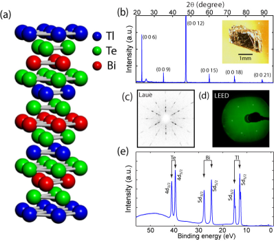
The crystal structure of Thallium based III-V-VI2 ternary chalcogenides is rhombohedra with the space group R-3m, which can be viewed as a distorted NaCl structure with four atoms in the primitive unit cell. A conventional unit cell of TlBiTe2 is shown in Fig. 1(a) as an example: the three different types of atoms stack in layers with repeating sequence …-Te-Bi-Te-Tl-…24 . The existence of a flat cleavage plane 25 parallel to the (111) surface in this family of compounds [inset of Fig. 1(b)] makes them suitable for ARPES study. The high quality of the crystal was demonstrated by the XRD [Fig. 1(b)] and Laue [Fig 1(c)] characterizations; and the LEED pattern on the sample surface after ARPES measurement (Fig. 1d) confirmed that the surface structure of the samples is free from reconstruction. The characteristic peaks of all three elements can be identified in core level photoemission measurements [Fig.1(e)].

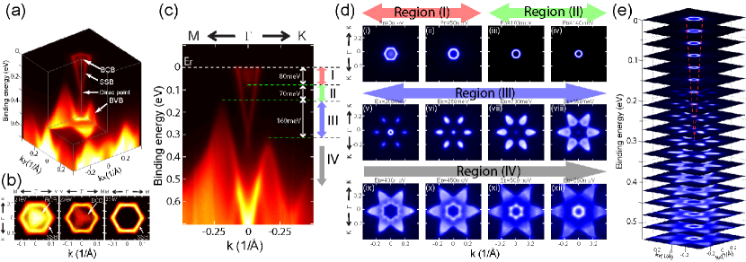
Figure 2 displays TlBiTl2 band structure around the center of the BZ. The 3D band structure [Fig.2(a)] shows a clear Dirac cone centered at the -point with broad features from bulk conduction (BCB) and bulk valence band (BVB) as theoretically predicted 21 ; 22 . To confirm the surface nature of the Dirac cone, excitation photon energy dependent ARPES study (Fig.2b) was performed. The non-varying shape of the outer hexagonal surface state band (SSB) FS with different excitation photon energies indicates its 2D nature; while the shape and the existence of the BCB FS pocket inside changes dramatically due to its 3D nature with strong dispersion as expected.
Detailed band dispersions along two high symmetry directions ( and ) are illustrated in Fig. 2(c), in which an asymmetry of the BVB along the two directions can be seen. Based on the characteristic energy positions of the bulk band, we can divide the band structure into four regions [Fig. 2(c)] for discussion of different FS geometries [Fig. 2(d)]. From region I to III, the bulk contribution of the FS evolves from an n-type pocket inside (region I) the n-type SSB FS to six p-type leaf-like pockets outside (Region III), with the bulk pockets disappear in region II; while in region IV, both the FS at the center and the surrounding leaf-like pockets are p-type. Fig. 2(e) shows a summary of the band evolution through all four regions.

Besides having the single Dirac cone on the surface, TlBiTe2 was also reported to superconduct when p-doped 23 , with of the corresponding density () resides in region III (about 150meV below the bottom of BVB). From our measurements, the FS geometry in this region is characterized by a ring like SSB FS and six surrounding p-type bulk pockets [Fig. 3(a)], as clearly shown in Fig. 2(d) - where a broad scan in -space that covers four BZs [Fig. 3(b)] confirms that the FS structure in Fig. 3(a) is the only feature within each BZ. This leads to the natural conclusion that the bulk superconductivity of p-type TlBiTe2 originates from the six leaf-like bulk pockets; and in the superconducting state, the surface state [the center FS pocket in Fig. 3(a,b)] can become superconducting due to the proximity effect induced by the bulk states. For such a superconductor, it has been proposed 14 that each vortex line has two Majorana zero modes related by the time reversal symmetry, thus making it a candidate for topological superconductors and suitable for the topological quantum computation 20 . However, the presence of superconductivity in p-type TlBiTe2 requires further confirmation 23.1 ; 23.2 .
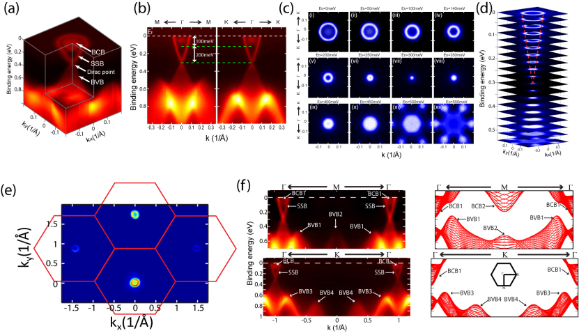
The band structures of TlBiTe2 in larger energy and momentum scale are shown in Fig. 3(c), where the measured dispersions (left sub-panels) along both and directions are compared with the corresponding calculation of the bulk band (right sub-panels). In general, the experimental dispersions along both directions agree well with the calculation, which reproduces each bulk feature of the measurement [Fig. 3(c)], albeit the relative energy position is slightly different. Again, the non-existence of the linear dispersion of the Dirac cone in the bulk calculation confirms its surface nature.
Interestingly, from the measurements [Fig. 3(c), top left panel], we find there is a small energy overlap (20meV) between the bottom of the electron pocket at M (BCB2) and the top of the valence band around (BVB1), indicating that TlBiTe2 is a semi-metal if resides in this region. Also, unlike the p-type sample, the FS of an n-type TlBiTe2 (electron density ) shows an electron pocket at the M point [Fig. 3(d)] due to the bulk conduction band (BCB2) at the zone boundary [Fig. 3(c), top row].

The band structure of TlBiSe2, another compound from the Tl-based ternary family, is summarized in Fig. 4. Similar to TlBiTe2, there exists a single surface Dirac cone at the point [Fig. 4(a-f)], confirming that its topological non-triviality. The main difference between TlBiSe2 and TlBiTe2 is that the Dirac point of TlBiSe2 resides at the top of the BVB [Fig. 4(a,b)], and the system has a 200meV direct bulk gap at . The bulk band structure is also simpler around and less anisotropic along -M and -K directions [Fig. 4(a,b)]. This simplicity is also shown in the constant energy contour plots [Fig. 4(c)] and its evolution [Fig. 4(d)]. Comparing Fig. 4(c) and Fig. 2(b), we notice that the SSB FS of TlBiSe2 is a convex hexagon, contrast to that of TlBiTe2 which shows slightly concave geometry. This difference resembles the difference between the SSB FSs of Bi2Te3 and Bi2Se3, and can be reflected by different observations in experiments such as scanning tunneling microscopy/spectroscopy STM/STS 28 ; 29 .
Besides the simpler band geometry around , the broad range FS map [Fig. 4(e)] of n-type TlBiSe2 is also simpler than that of the TlBiTe2 [Fig. 3(d)], without the electron pocket at the M point. This simplicity can also be seen in the band dispersions in Fig. 4(f), where although the experimental (left sub-panels) and calculated (right sub-panels) bulk band structure again show agreement in general, the BCB2 feature at M in the calculation (top right panel) was not seen in the measurements (top left panel), causing the missing of an electron pocket at M in Fig. 4e.
Acknowledgements We thank X. L. Qi, B.H. Yan and C.X. Liu for insightful discussions. This work is supported by the Department of Energy, Office of Basic Energy Science under contract DE-AC02-76SF00515.
References
- (1) X. L. Qi and S. C. Zhang, Phys. Today 63, 33 (2010)
- (2) A. Bernevig, T. L. Hughes and S. C. Zhang, Science 314, 1757 (2006)
- (3) M. Konig et al., Science 318, 766 (2007)
- (4) H. Zhang, et al., Nature Phys. 5, 438 (2009).
- (5) Y. Xia, et al., Nature Phys. 5, 398 (2009).
- (6) Y. L. Chen, et al., Science 325 178 (2009)
- (7) L. Fu, C. L. Kane and E. J. Mele, Phys. Rev. Lett. 98, 106803 (2007)
- (8) X. L. Qi, T. L. Hughes and S. C. Zhang, Phys. Rev. B 78, 195424 (2008)
- (9) J. E. Moore and L. Balents, Phys. Rev. B 75, 121306(R) (2007).
- (10) R. Roy, Phys. Rev. B 79, 195321 (2009)
- (11) B. Seradjeh, J. E. Moore and M. Franz, Phys. Rev. Lett, 103, 066402 (2009)
- (12) F. Wilzcek, Nature, 458, 129 (2009)
- (13) X. L. Qi, T. L. Hughes, S. Raghu and S. C. Zhang, Phys. Rev. Lett. 102, 187001 (2009).
- (14) X. L. Qi, T. L. Hughes, and S. C. Zhang, Phys. Rev. B 81, 134508 (2010).
- (15) A. P. Schnyder, S. Ryu, A. Furusaki and A. W. W. Ludwig, Phys. Rev. B 78, 195125 (2008).
- (16) A. Kitaev, http://arxiv.org/abs/0901.2686 (2009)
- (17) R. Roy, http://arxiv.org/abs/0803.2868 (2008).
- (18) L. Fu and C. L. Kane, Phys. Rev. Lett. 100, 096407 (2008).
- (19) Y. S. Hor, J. G. Checkelsky, D. Qu, N. P. Ong and R. J. Cava, http://arxiv.org/abs/1006.0317 (2010)
- (20) F. Wilczek, Nature Phys. 5, 614-618 (2009).
- (21) C. Nayak, S. H. Simon, A. Stern, M. Freedman and S. D. Sarma, Rev. Mod. Phys. 80, 1083 (2008).
- (22) B. Yan, et. al., Euro. Phys. Lett. 90 37002 (2010)
- (23) H. Lin, et. al., http://arxiv.org/abs/1003.2615
- (24) R. Hein and E. Swiggard, Phys. Rev. Lett. 24, 53-55 (1970).
- (25) E. F. Hockings and J. G. White, Acta Crystallographica14, 328 (1961).
- (26) M. Ozer, K. M. Paraskevopoulos, A. N. Anagnostopoulos, K. Kokkou and E. K. Polychroniadis, Semicond. Sci. Technol. 13 86-92 (1998)
- (27) J. D. Jensen, J. R. Bruke, D. W. Ernst and R. S. Allgaier, Phys. Rev. B, 6, 319 (1972)
- (28) N. S. Popovich, V. K. Shura, V. P. Daikonov, I. M. Fita and G. G. Levchenko,Sol. Stat. Comm. 50, 979 (1984)
- (29) L. Fu, Phys. Rev. Lett. 103 266801 (2009)
- (30) Z. Alpichshev. et al., Phys. Rev. Lett. 104 016410 (2010)