Memory circuit elements: from systems to applications
Abstract
In this paper, we briefly review the concept of memory circuit elements, namely memristors, memcapacitors and meminductors, and then discuss some applications by focusing mainly on the first class. We present several examples, their modeling and applications ranging from analog programming to biological systems. Since the phenomena associated with memory are ubiquitous at the nanoscale, we expect the interest in these circuit elements to increase in coming years.
I Introduction
Currently, there is strong interest in circuit elements with history-dependent properties. These form a general class of memory elements diventra09a which includes memory resistors (memristors) chua71a , memory capacitors (memcapacitors) and memory inductors (meminductors). Quite generally, memristors, memcapacitors and meminductors can be considered as time- and history-dependent generalizations of their standard counterparts.
Mathematically, an th-order -controlled memory element is defined by the equations diventra09a
| (1) | |||||
| (2) |
Here, and are any two circuit variables (current, charge, voltage, or flux) denoting input and output of the system, is an -dimensional vector of internal state variables, is a generalized response, and is a continuous -dimensional vector function. Special interest is devoted to devices determined by three pairs of circuit variables: current-voltage (memristors), charge-voltage (memcapacitors), and flux-current (meminductors). Two other pairs (charge-current and voltage-flux) are linked through equations of electrodynamics, and therefore do not give rise to any new device. Devices defined by the relation of charge and flux (which is the integral of the voltage) are not considered as a separate group since such devices can be redefined in the current-voltage basis chua71a .
We stress first that these memory devices are dynamical systems, namely systems whose state and response may change in time. In typical applications, memory devices operate under the action of a time-dependent (not static) input. It is also worth noting that the relations (1) and (2) are quite general. In particular, they may define systems whose properties cannot be reproduced with standard resistors, capacitors and inductors. In other words, there is no possible combination of standard circuit elements that can reproduce the dynamical properties of certain memory elements. In this sense, memristors, memcapacitors and meminductors can be considered as “fundamental” circuit elements. However, at least in the case of memcapacitors and meminductors, the relations (1) and (2) may also represent some other systems whose dynamical properties can be simulated by an appropriate combination of standard (albeit possibly non-linear) elements (for examples of these, see, e.g., Refs. krems2010a, ; martinez09a, ). Nonetheless, these latter memory systems are still of great importance since they provide a complex functionality within a single electronic structure martinez09a .
The area of research of memristors is more advanced both technologically and theoretically than that of memcapacitors and meminductors. In fact, although some experimental systems have been identified as memcapacitive diventra09a ; krems2010a ; martinez09a ; driscoll09a ; Lai09a and meminductive diventra09a , their number is still small and possible applications for them are less developed. In this review, we will then focus on memristors 222According to existing terminology, we will use the term memristors for both ideal memristors chua71a and memristive systems chua76a ..
It is convenient to introduce voltage-controlled and current-controlled memristors chua76a . An th-order current-controlled memristive system is described by the equations
| (3) | |||||
| (4) |
with again a vector representing internal state variables, and denote the voltage and current across the device, and is a scalar, called the memristance (for memory resistance). The equation for a charge-controlled (or ideal) memristor is a particular case of Eqs. (3) and (4), when depends only on charge, namely
| (5) |
with the charge related to the current via time derivative: .
We can also define an th-order voltage-controlled memristive system from the relations
| (6) | |||||
| (7) |
where we call the memductance (for memory conductance).
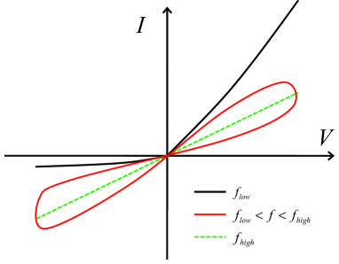
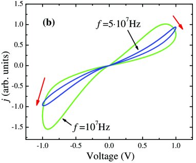
There are several common properties of memristors chua71a ; chua76a ; diventra09a . They are passive devices (provided or ) without an energy storage capability (unlike memcapacitors and meminductors which can store energy). Typically, at high frequencies, they behave as linear resistors and at low frequencies as non-linear resistors (assuming existence of a steady-state solution of Eq. (4) or (7)). A distinctive feature of well-defined memristors (with non-zero or ) is a pinched hysteresis loop on the current-voltage plane (see Fig. 1).
Because of the short format of this review, we are not able to include all topics concerning memristors or to cover the ones included in due detail. We will focus mainly on our results in this field and organize the text in the following order. Sec. II describes several different realizations of memristors. A theoretical modeling is discussed in Sec. III. We overview several important applications of memristors in Sec. IV. Finally, Sec. V presents our conclusions.
II Experimental Realizations
Many different systems exhibit memristive behavior. Early-identified memristor’s examples chua76a include thermistors sapoff63a and ionic systems hodgkin52a . Recent interest in memristor’s realizations has centered on nanoscale systems and nanostructures as we discuss below. Some of them were intensively studied in the context of development of resistive-switching memory during last 10-15 years. This area, to the best of our knowledge, was initiated by Hickmott in 1962 by the observation of hysteretic behavior in oxide insulators hickmott62a .
At the present time, it is well known that memristive effects can be observed in such diverse classes of materials as binary oxides (TiO2, CuO, NiO, CoO, Fe2O3, MoO, VO2) yang08a ; inoue08a ; lee07a ; seo04a ; driscoll09a ; driscoll09b , perovskite-type oxides (Pr1-xCaxMnO3, SrTiO3:Cr) asamitsu97a ; fors05a ; kim06a ; meijer05a ; nian07a , sulfides (Cu2S,Ag2S) terabe05a ; tamura06a ; waser07a , semiconductors (Si, GaAs, ZnSe-Ge) jo08a ; dong08a ; jo09a , spintronics materials pershin08a ; pershin09a ; wang09a and organics stewart04a ; lai05a ; alibart10a . In this review, we limit our discussion to the binary oxide TiO2 and spintronics systems. We will also discuss a memristor emulator pershin09d ; pershin09c - an electronic module simulating the memristor behavior.
II.1 Binary oxides materials
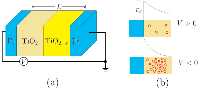
TiO2 is an example of binary oxide showing bipolar resistive switching. Recently, a memristive mechanism of its switching behavior has been identified strukov08a ; yang08a . It was suggested that the switching involves changes to the electronic barrier at the Pt/TiO2 interface induced by drift of oxygen vacancies under an applied electric field. When vacancies drift toward the interface, they create conducting channels that short-circuit the electronic barrier. When vacancies drift away from the interface they eliminate these channels, restoring the original electronic barrier yang08a . This material demonstrates promising characteristics for future ultra-high density memory applications such as fast read/write times (10ns), high on/off ratios (), suitable range of programming voltages, and possibility to fabricate small size cells.
II.2 Spintronic materials
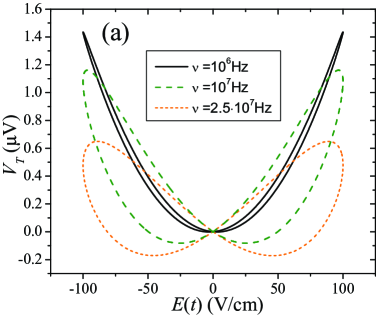
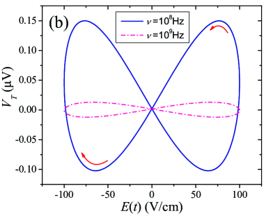
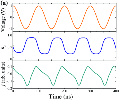
Semiconductor spintronic systems zutic04a were identified as memristive systems by Pershin and Di Ventra pershin08a . In semiconductor spintronics, memory effects are completely due to the electron spin degree of freedom. When an external control parameter changes, it takes time for the electron spin polarization to adjust to a new control parameter value (typically, the equilibration is governed by electron-spin diffusion and relaxation processes). Therefore, if a system’s resistivity depends on the level of electron spin polarization (as in semiconductor-ferromagnet junctions pershin07a ; pershin08b ) then such a system is fundamentally memristive pershin08a . Moreover, memory effects were predicted for spin Hall effect systems with inhomogeneous charge density distribution transverse to the driving electric field pershin09a . It is interesting that in this case memory effects can be observed directly in the transverse voltage. Fig. 2 shows transverse voltage hysteresis loops that demonstrate typical memristive behavior: non-linear dependence at low frequencies, pronounced hysteresis at higher frequencies and hysteresis collapse at very high frequencies pershin09a .
In metal spintronics, spin torque transfer known for a long time berger78a ; slonczewski96a ; tsoi98a ; myers99a can also be categorized as memristive. In spin torque transfer systems, the resistance is determined by the relative magnetization between opposite sides of a magnetic tunnel junction. Current flowing through the junction induces spin torque, in turn changing the relative magnetization. Krzysteczko et al. krzysteczko09a fabricated a modified magnetic tunnel junction with a resistive switching material inside. A spintronic memristor based on spin-torque-induced magnetization motion was discussed by Wang et al. wang09a .
II.3 Memristor emulator
A memristor emulator is an electronic module composed of standard (off-the-shelf) electronic components whose circuit response imitates that of memristor. Memristor emulator consisting of a microcontroller-controlled digital potentiometer and an analog-to-digital converter was recently demonstrated pershin09d ; pershin09c . Using the analog-to-digital converter, the microcontroller obtains information about the voltage applied to the memristor emulator and updates the digital potentiometer resistance using equations of voltage-controlled (Eqs. (6,7)) or current-controlled (Eqs. (3,4)) memristive systems. From the point of view of the external circuit, the memristor emulator is then a black box with two connections that operates exactly as a memristor. Its low cost, simplicity and flexibility make it useful for building prototype circuits with memrsistors for both research and education. Moreover, using the memristor emulator (which could be replaced by a real memristor), modules showing memcapacitive or meminductive behavior have also been demonstrated pershin09e .
III Theoretical description
For practical use of memory elements, the ability to predict their dynamics in electronic circuits is important. For this purpose, it is necessary to know the functions and entering Eqs. (1,2) that can be later used, for example, in SPICE modeling Benderli2009-1 ; Biolek2009-1 ; Biolek2009-2 . Generally, these functions can be constructed phenomenologically or derived from an appropriate physical analysis. Although models of resistive-switching devices were suggested before 2008 rozenberg04a , the realization that these devices belong to the class of memristive systems strukov08a has spurred further progress in understanding their behavior strukov09a ; strukov09b ; joglekar09a . Below, we consider a phenomenological model of memristor suggested by two of us (YVP and MD) to explain the learning properties of unicellular organisms pershin09b and a computationally simple tunneling barrier model. The tunneling barrier model includes both activation-type of internal state variables dynamics and electron tunneling through the barrier and it is indeed a physical realization of the above phenomenological model. It is also useful to understand the memory resistive properties of several systems of present interest.
III.1 Phenomenological model
A phenomenological model of a memristor has been suggested in Ref. pershin09b, . This model captures two very important experimental features of TiO2 memristorsyang08a : i) the fact that the resistance changes between two limiting values and , and ii) a threshold-type resistance dynamics. The latter is manifested in the following experimental observation yang08a : at low applied voltages the resistance of the memristor changes slowly while at high applied voltages its change is fast. The phenomenological model describes a voltage-controlled memristor (see Eqs. (6, 7)) with in Eq. (6) and Eq. (7) written as (with the memristance acquiring the limiting values and ) pershin09b
| (8) | |||||
where and are constants defining the memristance rate of change below and above the threshold voltage ; is the voltage across the memristor, and is the step function. This model has been used in several cases ranging from modeling of learning to emulators pershin09b ; pershin09d ; pershin09e . Moreover, similar models can be applied to memcapacitors and meminductors diventra09a .
III.2 Tunneling Barrier Model
Quite generally, let us assume that the electron transport through a voltage-controlled memristor involves a quantum mechanical tunneling through a barrier whose width and height are determined by internal state variables of the device. A particular example of application of this model regards the Pt/TiO2/Pt thin-film memristor yang08a , in which a Schottky barrier plays the role of the tunneling barrier and the internal state variable is the density of oxygen vacancies in the Schottky barrier region. For the sake of clarity we then focus on this particular system. We also note that the Schottky barrier was not explicitly included in previous titanium dioxide memristor models strukov08a ; strukov09b .
III.2.1 Dynamics of Internal State Variables
The structure of a TiO2 memristor is very simple yang08a , as shown in Fig. 3(a). It consists of two metallic (e.g., platinum) electrodes separated by a titanium dioxide thin film containing a region with a high concentration of oxygen vacancies, that we denote with TiO2-x, with describing the vacancies concentration. The right contact in Fig. 3(a) of the TiO2-x region with Pt can be considered as ohmic yang08a . The left contact (TiO2 with Pt) involves a Schottky barrier yang08a .
A fraction of oxygen vacancies can be moved from the TiO2-x region to the rest of TiO2 by an applied electric field via the phenomenon of electro-migration (see, e.g., Ref. Maxbook, ). Let us consider only mobile vacancies and track only the total number of mobile vacancies in the Schottky barrier region that extends inside of TiO2. Moreover, we assume that in our device the separation between Pt electrodes is of the order of two Schottky barrier lengths (here, by Schottky barrier length we mean its length when the device is in its high-resistance state). Only the vacancies in the Schottky barrier region are important to us since they modify the shape of the barrier (this is schematically shown in Fig. 3(b)) influencing directly the electron transport through the device 333A more detailed modeling of vacancy dynamics is possible using diffusion equations strukov09b . However, in this case, simulations become much more computationally expensive..
The vacancy dynamics can be described by a rate equation
| (9) |
where is the applied voltage and are the number of mobile vacancies in the left (Schottky barrier) region and right, , remaining part of titanium dioxide. The total number of mobile vacancies is assumed to be constant (). At the initial moment of time, can take any value between and depending on the initial state of the system. Limiting cases and correspond to high-resistance and low-resistance states of the memristor, respectively.
The time taken for a vacancy to move from one region to another can be found using an activation-type expression for the drift velocity as proposed in Ref. strukov09a,
| (10) | |||||
where is the ion mobility, , is the temperature, is the elementary charge, is the potential period, and for the electric field we have used the approximation , where is the length of titanium dioxide material. The derivation of Eq. (10) is based on the assumption that the oxygen vacancies are confined by a periodic potential due to all other atoms in the solid along the migration path. The application of the external electric field deforms the potential reducing the potential barrier between adjacent potential wells strukov09a . As a result, the expression for the drift velocity becomes very non-linear at strong applied fields strukov09a . Using Eq. (10), Eq. (9) can be rewritten as
| (11) |
where . A numerical solution of Eq. (11) is shown in Fig. 4a. Later, we use as an input parameter for tunneling current calculations.
III.2.2 Electron transport
Experimental data yang08a suggest that the tunneling current through the Schottky barrier is the main limiting factor to electron transport. This current can be approximated by a standard expression padovani66a
| (12) |
where is the classical Richardson constant, is the effective electron mass, and are constants. The expressions for and are different for forward and reverse biases. In particular, in the forward bias when electrons tunnel from TiO2 into the metal (expressions for and for the case of reverse bias can be found in Ref. padovani66a, ),
| (13) | |||
| (14) |
where is the barrier height, difference between work function of the metal and the affinity of the semiconductor, is the Fermi energy of the semiconductor and the energy is a material-dependent parameter that is inversely proportional to the Schottky barrier width padovani66a . For the sake of simplicity, a constant barrier height is assumed in our calculations. The tunneling through the barrier dominates thermionic emission and thermionic-field emission mechanisms when (the regime we consider here) sze_book1 .
We assume that the Schottky barrier width, , changes linearly with the number of the oxygen vacancies drifted to the Schottky barrier region of the device, that is where is a constant. Therefore, the maximum width of the Schottky barrier is and the minimum width is . As the energy is inversely proportional to (see Ref. padovani66a, ), we can write that where is the value of at . Fig. 4b depicts memristor’s curves obtained using Eq. (12). These curves have a shape typical of the memristor pinched hysteresis loop as anticipated in Fig. 1 and typical memristor’s frequency behavior.
IV Applications
Potential applications of memristors are envisioned in both digital and analog domains. Of great importance among digital applications are non-volatile solid-state memory, signal processing and programmable logic strukov07a ; xia09a . Analog applications of memristors are based on the possibility to continuously vary their resistance and, therefore, on their ability to store more information than in the digital regime. Analog applications include analog signal processing, learning circuits, programmable analog circuits and neuromorphic circuits. Below we discuss several analog applications of memristors pershin09b ; pershin09c ; pershin09d .
IV.1 Learning circuits
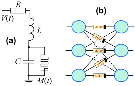
Quite generally, a “learning circuit” is an electronic circuit whose response at a given time adapts according to signals applied to the circuit at previous moments of time pershin09b . Memristors are ideal components for such a circuit as they provide non-volatile information storage and compatibility (as a time-dependent resistor) with other circuit elements. Two of us (YVP and MD) have recently suggested pershin09b a learning circuit which mimics adaptive behavior of the slime mold Physarum polycephalum from the group of amoebozoa. This work was inspired by an interesting experimental observation saigusa08a : when Physarum polycephalum is exposed to a pattern of periodic environmental changes, it learns and adapts its behavior in anticipation of the next stimulus to come. It was demonstrated pershin09b that such behavior can be described by the response of a simple electronic circuit shown in Fig. 5a composed of an LC contour and a memristor in parallel with the capacitor. The memristive function employed in that work is Eq. 8. When a periodic signal is applied to the learning circuit, the voltage across the capacitor significantly changes and can exceed the threshold voltage of the memristor. This leads to an increase in the resistance of memristor and, consequently, in a smaller damping of the LC contour. Therefore, the LC contour oscillations are maintained for a longer period of time in analogy with the same type of behavior as the amoeba’s when subject to periodical environment changes.
IV.2 Neuromorphic circuits
Neuromorphic circuits are circuits whose operation is meant to mimic that of the brain. In these circuits, memristors can be used as synapses whose role is to provide connections between neurons and store information. The small size of solid-state memristors is highly beneficial for this application since memristors’ density can be of the same order of magnitude as the density of synapses in human brains snider08a . Therefore, using memristors, the fabrication of an artificial neural network of a similar size of a biological brain becomes possible.
Typically, an artificial neural network consists of many artificial neurons connected by artificial synapses as we show schematically in Fig. 5b. The first memristor-based neural network realized experimentally pershin09c contained only three neurons connected by two synapses. However, we (YVP and MD) have shown that even such a small network could perform a fundamental property of the human brain: associative memory. Associative memory is closely related to the so-called Pavlovian training pavlov27a in which a particular response to a given stimulus develops. The most notable experiment of associative memory is that of a dog to which food is shown and, at the same time, the tone of a bell is rang so that, with time, the dog salivates at the ring of the bell only. In the electronic 3-neuron network demonstrated in Ref. pershin09c , two input neurons were responsible for the “sight of food” and “sound” events, while the output neuron generated a “salivation” command. It was shown that, if one starts with an untrained state of the synapse connecting the input “sound” neuron and output neuron and exposes the neural network to “sight of food” and “sound” signals simultaneously then an association between “food” and “sound” develops and an output signal is generated when only the “sound” input signal is applied.
IV.3 Programmable analog circuits
In programmable analog circuits, memristors can be used as digital potentiometers pershin09d . The main idea is to apply small amplitude voltages to memristors when they are used as analog circuit elements and high amplitude voltage pulses for the purpose of memristor’s resistance programming. Since the state of memristor appreciably changes only when the voltage applied to it exceeds a certain threshold strukov09a , the resistance of memristor is constant in the analog mode of operation and changes by discrete values with each voltage pulse. Using this idea, several programmable analog circuits demonstrating memristor-based programming of threshold, gain and frequency were demonstrated pershin09d .
V Conclusions and outlook
As this short review has shown, memory circuit elements are new promising components for future electronics. Their advantage is based on a combination of a history-dependent behavior with properties of a basic circuit element (such as resistance, capacitance or inductance). Of equal importance is the possibility of realizing memory elements at the nanoscale. The cost of certain implementations of these elements should be low because of their simple structure. We therefore anticipate that as memristors, memcapacitors and meminductors possibly develop into commercially available products in the coming years, novel exciting applications will be developed with impact not only for technology but also for fundamental science.
Acknowledgments
This work has been partially funded by the NSF grant No. DMR-0802830.
References
- (1) M. Di Ventra, Y. V. Pershin, and L. O. Chua, Proc. IEEE 97, 1717 (2009)
- (2) L. O. Chua, IEEE Trans. Circuit Theory 18, 507 (1971)
- (3) M. Krems, Y. V. Pershin, and M. Di Ventra, arXiv:1001.0796(2010)
- (4) J. Martinez-Rincon, M. Di Ventra, and Y. V. Pershin, Phys. Rev. B (in press); arXiv:0912.4921(2009)
- (5) T. Driscoll, H.-T. Kim, B.-G. Chae, B.-J. Kim, Y.-W. Lee, N. M. Jokerst, S. Palit, D. R. Smith, M. Di Ventra, and D. N. Basov, Science 325, 1518 (2009)
- (6) Q. Lai, L. Zhang, Z. Li, W. F. Stickle, R. S. Williams, and Y. Chen, Appl. Phys. Lett. 95, 213503 (2009)
- (7) According to existing terminology, we will use the term memristors for both ideal memristors chua71a and memristive systems chua76a .
- (8) L. O. Chua and S. M. Kang, Proc. IEEE 64, 209 (1976)
- (9) M. Sapoff and R. M. Oppenheim, Proc. IEEE 51, 1292 (1963)
- (10) A. L. Hodgkin and A. F. Huxley, Journal of Physiology 117, 500 (1952)
- (11) T. W. Hickmott, J. Appl. Phys. 33, 2669 (1962)
- (12) J. J. Yang, M. D. Pickett, X. Li, D. A. A. Ohlberg, D. R. Stewart, and R. S. Williams, Nat. Nanotechnol. 3, 429 (2008)
- (13) I. H. Inoue, S. Yasuda, H. Akinaga, and H. Takagi, Phys. Rev. B 77, 035105 (2008)
- (14) D. Lee, D. jun Seong, I. Jo, F. Xiang, R. Dong, S. Oh, , and H. Hwang, Appl. Phys. Lett. 90, 122104 (2007)
- (15) S. Seo, M. J. Lee, D. H. Seo, E. J. Jeoung, D.-S. Suh, Y. S. Joung, I. K. Yoo, I. R. Hwang, S. H. Kim, I. S. Byun, J.-S. Kim, J. S. Choi, and B. H. Park, Appl. Phys. Lett. 85, 5655 (2004)
- (16) T. Driscoll, H.-T. Kim, B. G. Chae, M. Di Ventra, and D. N. Basov, Appl. Phys. Lett. 95, 043503 (2009)
- (17) A. Asamitsu, Y. Tomioka, H. Kuwahara, and Y. Tokura, Nature 388, 50 (1997)
- (18) R. Fors, S. I. Khartsev, and A. M. Grishin, Phys. Rev. B 71, 045305 (2005)
- (19) D. S. Kim, Y. H. Kim, C. E. Lee, and Y. T. Kim, Phys. Rev. B 74, 174430 (2006)
- (20) G. I. Meijer, U. Staub, M. Janousch, S. L. Johnson, B. Delley, and T. Neisius, Phys. Rev. B 72, 155102 (2005)
- (21) Y. B. Nian, J. Strozier, N. J. Wu, X. Chen, and A. Ignatiev, Phys. Rev. Lett. 98, 146403 (2007)
- (22) K. Terabe, T. Hasegawa, T. Nakayama, and M. Aono, Nature 433, 47 (2005)
- (23) T. Tamura, T. Hasegawa, K. Terabe, T. Nakayama, T. Sakamoto, H. Sunamura, H. Kawaura, S. Hosaka, and M. Aono, Jpn. J. Appl. Phys. 45, L364 (2006)
- (24) R. R. Waser and M. Aono, Nat. mat. 6, 833 (2007)
- (25) S. H. Jo and W. Lu, Nano Lett. 8, 392 (2008)
- (26) Y. Dong, G. Yu, M. C. McAlpine, W. Lu, and C. M. Lieber, Nano Lett. 8, 386 (2008)
- (27) S. H. Jo, K.-H. Kim, and W. Lu, Nano Lett. 9, 870 (2009)
- (28) Y. V. Pershin and M. Di Ventra, Phys. Rev. B 78, 113309 (2008)
- (29) Y. V. Pershin and M. Di Ventra, Phys. Rev. B 79, 153307 (2009)
- (30) X. Wang, Y. Chen, H. Xi, H. Li, and D. Dimitrov, El. Dev. Lett. 30, 294 (2009)
- (31) D. R. Stewart, D. A. A. Ohlberg, P. A. Beck, Y. Chen, R. S. Williams, J. O. Jeppesen, K. A. Nielsen, and J. F. Stoddart, Nano Lett. 4, 133 (2004)
- (32) Y.-S. Lai, C.-H. Tu, D.-L. Kwong, and J. S. Chen, Appl. Phys. Lett. 87, 122101 (2005)
- (33) F. Alibart, S. Pleutin, D. Guerin, C. Novembre, S. Lenfant, K. Lmimouni, C. Gamrat, and D. Vuillaume, Adv. Funct. Mat. 20, 330 (2010)
- (34) Y. V. Pershin and M. Di Ventra, IEEE Trans. Circ. Syst. I (in press); arXiv:0908.3162(2009)
- (35) Y. V. Pershin and M. Di Ventra, Neural Networks (in press); arXiv:0905.2935(2009)
- (36) D. B., G. S. Snider, D. R. Stewart, and R. S. Williams, Nature 453, 80 (2008)
- (37) I. Žutić, J. Fabian, and S. Das Sarma, Rev. Mod. Phys. 76, 323 (2004)
- (38) Y. V. Pershin and M. Di Ventra, Phys. Rev. B 75, 193301 (2007)
- (39) Y. V. Pershin and M. Di Ventra, Phys. Rev. B 77, 073301 (2008)
- (40) L. Berger, J. Appl. Phys. 49, 2156 (1978)
- (41) J. C. Slonczewski, J. Magn. Magn. Mat. 159, L1 (1996)
- (42) M. Tsoi, A. G. M. Jansen, J. Bass, W.-C. Chiang, M. Seck, V. Tsoi, and P. Wyder, Phys. Rev. Lett. 80, 4281 (1998)
- (43) E. B. Myers, D. C. Ralph, J. A. Katine, R. N. Louie, and R. A. Buhrman, Science 285, 867 (1999)
- (44) P. Krzysteczko, G. Reiss, and A. Thomas, Appl. Phys. Lett. 95, 112508 (2009)
- (45) Y. V. Pershin and M. Di Ventra, Electronics Letters 46, 517 (2010)
- (46) S. Benderli and T. A. Wey, Electron. Lett. 45, 377 (2009), ISSN 0013-5194
- (47) Z. Biolek, D. Biolek, and V. Biolkova, Radioengineering 18, 210 (2009), ISSN 1210-2512
- (48) Z. Biolek, D. Biolek, and V. Biolkova, Proc. of ECCTD ’09, European Conference on Circuit Theory and Design, 249(August 23-27, 2009)
- (49) M. J. Rozenberg, I. H. Inoue, and M. J. Sanchez, Phys. Rev. Lett. 92, 178302 (2004)
- (50) D. B. Strukov and R. S. Williams, Appl. Phys. A-Mater. Sci. Process. 94, 515 (2009)
- (51) D. B. Strukov, J. L. Borghetti, and R. S. Williams, Small 5, 1058 (2009)
- (52) Y. N. Joglekar and S. J. Wolf, Eur. J. Phys. 30, 661 (2009)
- (53) Y. V. Pershin, S. La Fontaine, and M. Di Ventra, Phys. Rev. E 80, 021926 (2009)
- (54) M. Di Ventra, Electrical Transport in Nanoscale Systems (Cambridge University Press, 2008)
- (55) A more detailed modeling of vacancy dynamics is possible using diffusion equations strukov09b . However, in this case, simulations become much more computationally expensive.
- (56) F. A. Padovani and R. Stratton, Solid-State Electron. 9, 695 (1966)
- (57) S. M. Sze and K. K. Ng, Physics of Semiconductor Devices, 3rd ed. (Wiley-Interscience, 2006)
- (58) D. Strukov and K. Likharev, IEEE Trans. Nanotechnology 6, 696 (2007)
- (59) Q. Xia, W. Robinett, M. W. Cumbie, N. Banerjee, T. J. Cardinali, J. J. Yang, W. Wu, X. Li, W. M. Tong, D. B. Strukov, G. S. Snider, G. Medeiros-Ribeiro, and R. S. Williams, Nano Letters 9, 3640 (2009)
- (60) T. Saigusa, A. Tero, T. Nakagaki, and Y. Kuramoto, Phys. Rev. Lett. 100, 018101 (2008)
- (61) G. S. Snider, SciDAC Review 10, 58 (2008)
- (62) I. Pavlov, Conditioned Reflexes: An Investigation of the Physiological Activity of the Cerebral Cortex (London: Oxford University Press, 1927) (translated by G. V. Anrep)