Intervalley Coupling for Interface-Bound Electrons in Silicon:
An Effective Mass Study
Abstract
Orbital degeneracy of the electronic conduction band edge in silicon is a potential roadblock to the storage and manipulation of quantum information involving the electronic spin degree of freedom in this host material. This difficulty may be mitigated near an interface between Si and a barrier material, where intervalley scattering may couple states in the conduction ground state, leading to non-degenerate orbital ground and first excited states. The level splitting is experimentally found to have a strong sample dependence, varying by orders of magnitude for different interfaces and samples. The basic physical mechanisms leading to such coupling in different systems are addressed here. We expand our recent study based on an effective mass approach, incorporating the full plane wave (PW) expansions of the Bloch functions at the conduction band minima. Physical insights emerge naturally from a simple Si/barrier model. In particular, we present a clear comparison between ours and different approximations and formalisms adopted in the literature, and establish the applicability of these approximations in different physical scenarios.
pacs:
03.67.Lx, 85.30.-z, 85.35.Gv, 71.55.CnI Introduction
Electronic spins in Si are promising candidates for qubits due to their naturally long coherence times. Das Sarma et al. (2004) An important challenge for using electronic spins as qubits in silicon devices is to assure that the low energy physics is ruled solely by the 2-level spin degree of freedom. Rahman et al. (2009); Culcer et al. (2010a, b); Debernardi and Fanciulli (2010); Li et al. (2010); Wang et al. (2010); Koenraad and Flatte (2011); Escott et al. (2010); Rahman et al. (2011); Raith et al. (2011) In bulk Si crystal, the conduction band lower edge is six-fold degenerate. Any superposition of the six Bloch states associated with the minima in along the , and crystallographic directions is also an eigenstate of the crystalline hamiltonian, so that the orbital state of a free conduction electron at the band edge is normally not defined.
Several quantum computer architectures under investigation involve manipulation of the electronic spin at an interface between Si and some barrier material, most commonly SiGe alloys Friesen et al. (2003); Eriksson et al. (2004) and SiO2 Kane (1998, 2000) barriers. The confining electric field (generated by external electrostatic gates and/or depletion layers) generates a quasi-triangular potential well at the interface. Assuming the interface to be perpendicular to the direction [that is, a (001) interface], the ground state energy of such triangular potential well depends on the effective mass in the direction. The effective masses at the conduction band minima of Si are anisotropic, with the longitudinal effective mass more than 4 times larger than the transversal. This shifts the minima along the and directions well above the minima in the direction, breaking the six-fold degeneracy into a 2-fold degenerate ground state and a 4-fold degenerate excited state. Ando et al. (1982); Kane et al. (2000) The splitting is further enhanced if tensile strain is applied to the Si crystal (e.g. in Si quantum wells grown over relaxed SiGe substrates). Herring and Vogt (1956) The degeneracy in the two-dimensional subspace is lifted in the presence of a sufficiently singular perturbation potential, such as a Si/barrier interface. Saraiva et al. (2009) Experimental values of the valley splitting in interfaces have been reported in the 0.1 to 1 meV range. Ando et al. (1982); Goswami et al. (2007) A peculiar result was reported by Takashina et al., Takashina et al. (2006) who measured a “giant” splitting of 23 meV on a Si/SiO2 interface in a SIMOX (separation by implantation of oxygen) structure.
In the presence of orbital degeneracy, electron manipulations relying on the Pauli’s exclusion principle, such as Heisenberg exchange coupling Loss and DiVincenzo (1998) and spin blockade Ono et al. (2002), may become unreliable since the qubits Hilbert Space is now spanned by the valley as well as the spin degrees of freedom. For an electron spin qubit confined in a Si quantum dot, reliable knowledge of the interface induced valley splitting is crucial. Friesen et al. (2003) For example, for a single electron spin qubit, Loss and DiVincenzo (1998) if the valley splitting is smaller than the reservoir thermal energy, or valley splittings are different across two quantum dots, exchange gates cannot be performed as was originally designed since two-valley two-electron singlet and triplet states (where the two electrons are in different valleys) are not exchange-split. Li et al. (2010) When two-electron singlet and triplet states are used to encode a logical qubit, reliable initialization becomes impossible if valley splitting in a quantum dot is unknown or known to be small (compared to reservoir temperature energy scale). Culcer et al. (2009) In short, clear knowledge of a large valley splitting in a Si quantum dot is imperative to assure the feasibility of an electron spin qubit.
Early theoretical studies on Si valley splitting in the framework of the EMA were performed more than 30 years ago. Ohkawa and Uemura (1977); Sham and Nakayama (1979) The relevance of the periodic part of the Si bulk Bloch states (leading to the so-called Umklapp processes) to this scattering became clear in the 70’s. Resta (1977) However, its inclusion combined with the EMA formalism leads to a puzzling dependence of calculated physical properties on the particular position of the barrier within the range of separation between atomic layers, an artifact already found in previous works Sham and Nakayama (1979) which is discussed in detail and clarified in Ref. Saraiva et al., 2009. These early theoretical studies do not discuss the strong sample dependence observed experimentally.
Valley mixing has been extensively studied in the literature Ando et al. (1989); Ando and Akera (1989); Ando (1995); Menchero et al. (1999) regarding GaAs/AlAs or GaAs/GaAlAs interfaces and superlattices. The most relevant valley mixing in this context involves the -valleys of the electron conduction band in the AlAs layer, which is the global band minimum in AlAs and a local minimum in GaAs, and the -valley in the GaAs layer. This mixing involves separated spatial layers. Higher and states in AlAs and GaAs also intervene in the mixing Ando and Akera (1989). In Si, mixing occurs between the crystalline momenta and in the same spatial layer, that is, in the Si slab, and is due to the barrier potential alone. The theory and experimental consequences of GaAs/AlAs valley mixing are thus different and not transferrable to Si.
Performing a fully ab initio treatment is not realistic in the study of valley coupling in Si due to limitations both on the length and on the energy scales. Intervalley splittings of the order of tenths of meV would not be accurately resolved within the density functional theory (DFT) approach based on current computational resources. Also, the electronic states under study spread over several lattice parameters, and simulation of large supercells with appropriate description of the band gap (through Hedin’s GW scheme, Hedin (1965) for example), again involve numerical computations beyond currently available capability.
More recent investigations often employ approaches with atomistic ingredients, whether based completely on the tight-binding (TB) method or on the hybrid of TB and EMA. Grosso et al. (1996); Boykin et al. (2004a, b); Friesen et al. (2006); Nestoklon et al. (2006); Lee and von Allmen (2006); Kharche et al. (2007); Boykin et al. (2008); Srinivasan et al. (2008) These atomistic methods allow treatment of disorder effects directly. For example, TB and EMA+TB calculations conclude that for tilted Si/SiGe quantum wells, alloy disorder and interfacial step disorder must be included to obtain finite valley splittings. Friesen et al. (2006); Kharche et al. (2007) Such sample-dependent results are consistent with the observed variation of this coupling as measured in different interfaces. On the other hand, the detailed description of disorder comes at the expense of generality and prevents analytical insights since these methods require numerical treatment (with exceptions, some of which are discussed in Sec. IV.2).
We have recently performed Saraiva et al. (2009) a study of the valley splitting problem that leads to the identification of relevant physical mechanisms underlying the intervalley coupling. Our EMA model incorporates the atomistic Bloch functions obtained from ab initio calculations in connection with an envelope function obtained from the single valley EMA equation. That study focused on the relevance of the barrier height and the interface width.
In the present work, we discuss the ab initio results which are required in implementing our approach. In particular, we provide a detailed roadmap to the connection between effective mass and and the ab initio wavefunction, deriving the formalism and discussing the physics and applicability of our methodology. Further results are presented and discussed, including a more complete analysis of the role of the confining electric field perpendicular to the interface plane. The plane wave (PW) expansion of the periodic part of each Bloch function is explicitly given, and contributions from reciprocal lattice vectors in the PW expansion are analyzed, identifying the most relevant Umklapp processes. We also discuss the present model in the context of existing studies and compare our results with previous ones whenever warranted. The interface is modeled here within EMA by a finite height step potential. Other interface profiles were already considered in our previous study. Saraiva et al. (2009)
In section II we briefly review the model, emphasizing the assumptions involved in the derivation of the formalism. We proceed to numerically calculate the coupling under various electric fields and conduction band offsets in section III. These results allow comparison of the valley coupling in different experimental conditions, and to discuss possible mechanisms contributing to the giant splitting reported in Ref. Takashina et al., 2006. Comparison of our theoretical approach with others in the literature is given in section IV, where we also evaluate some of the approximations adopted in previous works and shed light in some theoretical questions, such as the range of applicability of various EMA treatments. Finally, our conclusions are presented in section V.
II Theoretical Background
We consider a single electron at the bottom of the Si conduction band, near a (001) Si/barrier interface. Assuming translational symmetry in the plane, we model the barrier material as an effective potential mimicking the conduction band offset along the direction. This model addresses only the position in energy of the bottom of the conduction band, disregarding the detailed electronic structure in the transition region between Si and the barrier material, as we discuss below.
The Hamiltonian for the conduction band electron is assumed to be of the form
| (1) |
where is the unperturbed bulk Si Hamiltonian and is the barrier potential. An electric field along the direction keeps the electron close to the interface. The dielectric function changes from the bulk Si value to the bulk barrier material value and, in a more accurate analysis, could include many-body effects.
A sequence of approximations are involved in obtaining the EMA equation for Si heterostructures. The first assumption involves the expansion of the electronic wavefunction in terms of the periodic part of Bloch states around the conduction band minima, assumed to be the same for both the well semiconductor and the barrier material. Bastard (1988) The envelope function approach is better justified if the wavevectors at the minima of the two materials are relatively near relative to the Brillouin zone dimensions.
We further assume their effective masses to be the same, although it is possible within EMA to account for different effective masses in heterostructures. Bastard (1988) We avoid specifying the barrier material and systematically investigate the effects of the barrier height alone.
Finally, the crystalline structure is assumed to be preserved across the interface. In a MOSFET geometry, SiO2 grown over Si is typically amorphous, as different metastable crystalline phases coexist, with crystallographic directions that do not necessarily match the directions of the Si slab. Helms and Poindexter (1994) Moreover, the most energetically favorable crystalline phases of SiO2 have a single conduction band minimum at the point. Ramos et al. (2004) On the other hand, Si(1-x)Gex alloys at low concentrations of Ge () present conduction band minima at the same position in the Brillouin zone as pure Si crystal, Rieger and Vogl (1993) and the effective mass remains almost unchanged for the Ge concentration in the alloy up to . For samples under experimental investigation, Friesen et al. (2003) Si is epitaxially grown over a relaxed SiGe substrate, so that the crystallographic directions match. Although the conduction band states are not exactly the same for these two materials, they are expected to be very similar. Thus, for Si/SiGe heterostructures the EMA assumptions are better justified than for MOSFETs.
However, given the large conduction band offset between Si and SiO2 a very small penetration of the envelope function into the barrier material is expected. Detailed simulation of the electronic structure of Si/SiO2 interfaces is possible, but does not lead to general results, since different nanofabrication methods and small variations of the growth parameters lead to very different interface morphologies. Takashina et al. (2006); Takahashi et al. (1999) We adopt the EMA approach in the case of Si/SiO2 interface bearing in mind that this approximation could lead to quantitative inaccuracies that should be estimated using some other approach.
Within the above assumptions, one obtains the envelope function from the single-valley effective mass equation Bastard (1988)
| (2) |
where is the longitudinal effective mass for Si. The electronic eigenstates of Eq. (1) bound to the interface are obtained from the single-valley EMA Kohn (1957) as where are the Bloch wave vectors of the conduction band minima (). It is convenient to perform a PW expansion of the periodic functions Koiller et al. (2004) leading to the complete wavefunctions
| (3) |
where are reciprocal lattice vectors. The PW expansion in equation (3), originally explored in connection to Ref. Koiller et al., 2004, is useful in several other contexts. It was obtained from ab initio Density Functional Theory (DFT) calculations, Koiller et al. (2004) performed with the ABINIT code. Gonze et al. (2002) From a DFT perspective, the electronic correlations for the bulk Bloch states are described in the Local Density Approximation (LDA). Hohenberg and Kohn (1964); Kohn and Sham (1965) The exchange-correlation potential parameterized by Perdew and Zunger Perdew and Zunger (1981) from Ceperley-Alder quantum Monte-Carlo results for the homogeneous electron gas Ceperley and Alder (1980) was adopted. The interactions between valence electrons and ions are described by the ab-initio, norm-conserving pseudopotentials of Troullier-Martins, Troullier and Martins (1991) generated with the FHI98PP code. Fuchs and Scheffler (1999) These approximations significantly speed up the computation of the conduction band structure, with a PW expansion of the wavefunctions including terms up to 16 Ry, that is, corresponding to 290 plane waves for each , with virtually no computational effort. The calculated equilibrium lattice constant of Si at Å and the conduction-band minima at are in close agreement with experimental results. Madelung (1996) These values are used in the calculations presented below.
We find that over 90 of the spectral weight of the PW expansion in equation (3) comes from the five points in the BCC reciprocal lattice which are nearest to each conduction band minimum . The valley coupling
| (4) |
is the key quantity leading to the valley splitting . Saraiva et al. (2009) Therefore, a preliminary estimate of the intervalley coupling could involve 9 PWs (the point is a common nearest neighbor for both at the minima). The coefficients such that , accounting for 99.5 % of the spectral weight, are explicitly given for in Table 1; coefficients for all band minima may be obtained from those by symmetry (see Table caption).
| Re | Im | ||
|---|---|---|---|
| ( 1 -1 -1) | -0.3131 | -0.3131 | 0.1961 |
| (-1 1 -1) | -0.3131 | -0.3131 | 0.1961 |
| ( 1 1 -1) | -0.3131 | 0.3131 | 0.1960 |
| (-1 -1 -1) | -0.3131 | 0.3131 | 0.1960 |
| ( 0 0 0) | 0.3428 | -0.0000 | 0.1175 |
| ( 2 0 -2) | -0.0986 | 0.0000 | 0.0097 |
| ( 0 2 -2) | -0.0986 | 0.0000 | 0.0097 |
| (-2 0 -2) | -0.0986 | 0.0000 | 0.0097 |
| ( 0 -2 -2) | -0.0986 | 0.0000 | 0.0097 |
| ( 1 -1 1) | 0.0695 | -0.0695 | 0.0097 |
| (-1 1 1) | 0.0695 | -0.0695 | 0.0097 |
| ( 1 1 1) | 0.0695 | 0.0695 | 0.0097 |
| (-1 -1 1) | 0.0695 | 0.0695 | 0.0097 |
| (-2 2 -2) | -0.0000 | -0.0451 | 0.0020 |
| ( 2 -2 -2) | -0.0000 | -0.0451 | 0.0020 |
| (-2 -2 -2) | 0.0000 | 0.0451 | 0.0020 |
| ( 2 2 -2) | 0.0000 | 0.0451 | 0.0020 |
| ( 0 2 2) | 0.0387 | -0.0000 | 0.0015 |
| ( 2 0 2) | 0.0387 | -0.0000 | 0.0015 |
| ( 0 -2 2) | 0.0387 | -0.0000 | 0.0015 |
| (-2 0 2) | 0.0387 | -0.0000 | 0.0015 |
| ( 0 0 -4) | 0.0186 | -0.0000 | 0.0003 |
| (-1 1 3) | 0.0114 | 0.0114 | 0.0003 |
| ( 1 -1 3) | 0.0114 | 0.0114 | 0.0003 |
| (-1 -1 3) | 0.0114 | -0.0114 | 0.0003 |
| ( 1 1 3) | 0.0114 | -0.0114 | 0.0003 |
| ( 0 0 4) | 0.0121 | -0.0000 | 0.0001 |
| ( 3 -3 -1) | -0.0075 | -0.0075 | 0.0001 |
| (-3 3 -1) | -0.0075 | -0.0075 | 0.0001 |
| ( 3 3 -1) | -0.0075 | 0.0075 | 0.0001 |
| (-3 -3 -1) | -0.0075 | 0.0075 | 0.0001 |
We take for the step potential, which is the most favorable model for the conduction band profile between Si and the barrier in terms of maximizing the valley coupling. Saraiva et al. (2009) It is written as Bastard (1988)
| (7) |
where is the position of the interface and is the conduction band offset. The step potential aims at modeling a perfectly sharp interface, a concept that involves changing the species of the atomic constituents abruptly, i.e. across one monolayer (1ML). However, the envelope function equation allows a continuous choice of the interface position , even within 1 ML width, as discussed in Ref. Saraiva et al., 2009. Although is ill-defined within a ML length scale, it is convenient to keep this simple interface model for it allows decomposing the integral in equation (6) into terms that are easily identifiable, some of which are familiar from previous theoretical treatments. Other models of the interface have been studied in Ref. Saraiva et al., 2009.
In equation (6) we integrate by parts the term proportional to given in (7),
| (8) | |||||
| (9) | |||||
| (10) |
where we are interested in an interface bound state, so that the electronic density vanishes at . Three terms are left, labeled (8), (9) and (10) above. Term (8) evidences the role of the electronic density at the interface through a function at ; term (9) gives the contribution of the evanescent tail of the electronic envelope function into the barrier material ; term (10) represents an intervalley scattering induced directly by the electric field, which we find to be vanishingly small. Summation of these contributions over the reciprocal lattice vectors [see equation (5)] leads to three contributions to the intervalley coupling
| (11) |
that is, the delta-function contribution , the evanescent term contribution , and the electric field contribution .
Besides the mismatch between the conduction band minima of the two materials, we also consider the change in dielectric screening constant from the semiconductor to the insulator. The dielectric function is taken as and . Note that also introduces a kink in the electrostatic potential in the scale of the monolayer separation, which could in principle contribute to the intervalley coupling.
III Numerical Solution and Results
III.1 Envelope Function Variational Approaches: Finite Differences and Trial Function
The envelope function is obtained from equation (2), which has no analytic solution. The approach adopted to solve this equation must be carefully chosen, since the intervalley coupling depends explicitly on the envelope function details, as shown in equations (8), (9) and (10). The first term (8), which gives rise to in equation (11), is proportional to the electronic probability density at the interface, while the second term (9) depends on the envelope tail inside the barrier, defining the contribution of the evanescent tail. The term (10) is always found to be negligibly small compared to the others, and is not included in the results presented here.
In order to get an analytic approximation for the envelope function, we present initially results obtained using the variational approach; we tried several functional forms for the variational envelope function, all satisfying the following boundary conditions: in the far semiconductor region (), under a constant electric field, the envelope function is approximated by a gaussian decay; towards the barrier material the short range decay () is nearly exponential. The trial function that typically gave the lowest energy expectation value was
| (12) |
with (i=A,B).
If we take the barrier to be infinite, the optimized variational parameters become and . But in general the barriers are finite, some penetration is expected so that and . From the continuity conditions and , and the normalization , we obtain expressions for , , and in terms of the variational parameters and ; e.g. For , we have
| (13) |
| (14) |
| (15) |
where erfc is the complementary error function,
| (16) |
Analytic solutions for the case of may also be obtained. However, for the step function potential and at relatively large length scales, the interface position is irrelevant: it separates two semi-infinite regions, one filled with Si and the other with the barrier material. At atomic distance length scales, the coupling dependence on shows oscillatory behavior with a period of 1 ML, a peculiarity of the EMA combined with the underlying Bloch states, as discussed in detail in Ref. Saraiva et al., 2009. Data presented there (Figure 5 of Ref. Saraiva et al., 2009) indicate that, for the step potential, these oscillations cause an uncertainty of about in . In what follows, for simplicity and definiteness, we arbitrarily fix the value of bearing in mind that our results for the coupling are not accurate within up to .
In order to provide a more robust estimate of the wavefunction, independent of our choice of its functional form, we also solve equation (2) through a finite differences method. This approach allows us to obtain the wave function variationally without inputing a guess for the functional form of the envelope. The envelope function is discretized and the derivatives are approximated by the slope of the interpolated straight line between two discrete points. Each discrete point is taken as a separate variational parameter, under the constraint that the wave function is normalized. The minimum energy in this configuration space is obtained through the Steepest Descent method. This strategy should in principle permit us to discuss a wide range of electric fields.
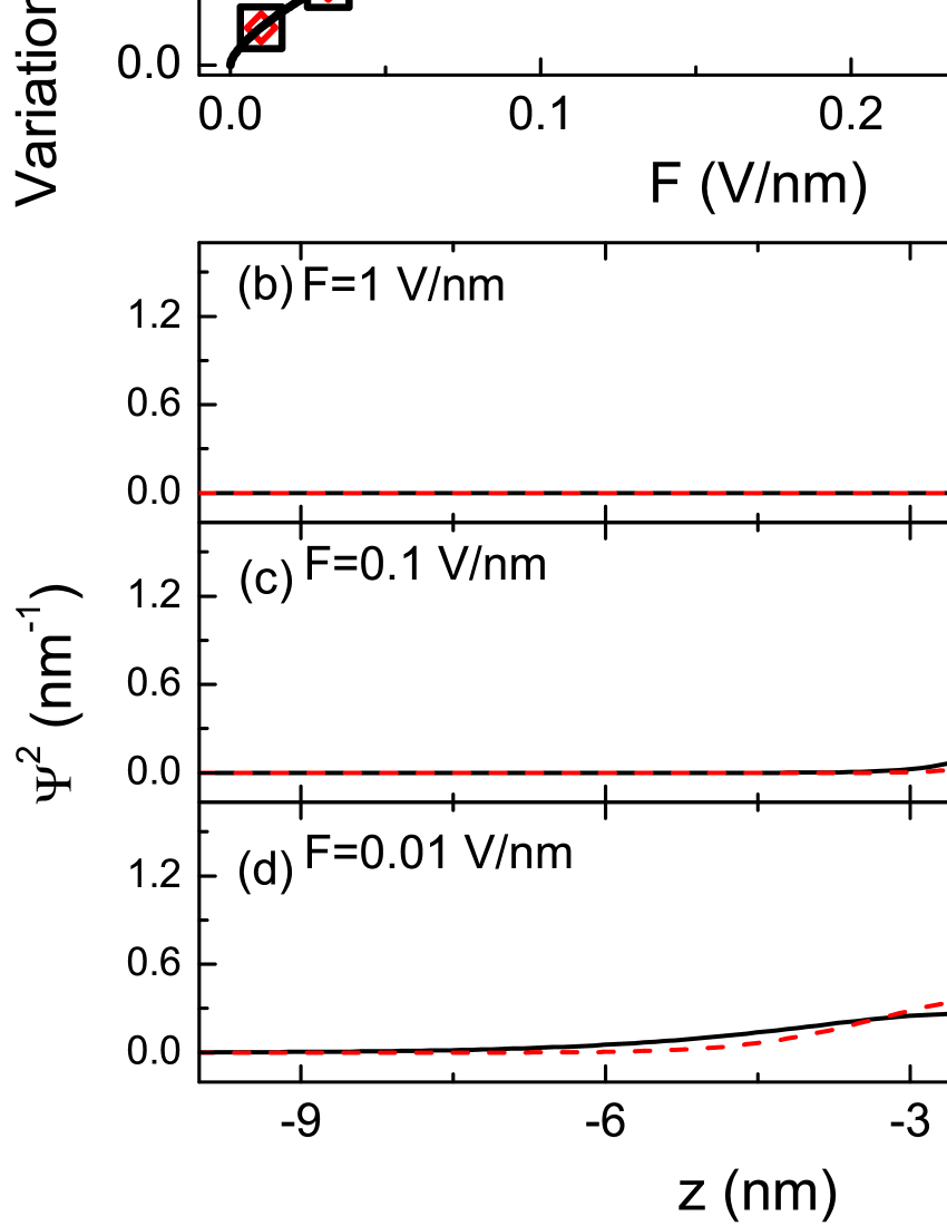
The trial function and the finite differences expectation value of the energy are given in Fig. 1(a), according to which the lowest value down to V/nm is obtained within finite differences/steepest descent method. The exact result for infinite barrier, given in Ref. Stern, 1972, is also included, and a good agreement with our numerical results is obtained. As the field increases and pushes the wavefunction towards the barrier, an evanescent tail into the barrier region is formed for eV, lowering the electronic energy with respect to the impenetrable barrier case, as expected [upper right data in Fig. 2(a)]. The good agreement for the expectation value of the energy among the three methods, for example at F=0.1 V/nm in Fig 1(a), does not imply that the wavefunctions are in agreement - as illustrated in Fig 1(c) and as is obvious for the infinite barrier case, where the wavefunction for is exactly zero. It is known that the energy alone is not a valid criterion to guarantee the wavefunction validity, in particular here for - from which the coupling is calculated. Imposing a predetermined form to the envelope most certainly will give spurious results for and . This points the numerical finite differences as the most adequate approach, with the additional capability of describing different interface profiles. Saraiva et al. (2009)
The finite differences approach is expected to be more accurate than trial-function based methods. However, in practice, numerical constraints limit its implementation and reliability. Below V/nm (not shown), we find that the lowest energy actually corresponds to Eq. (12), a consequence of our numerical accuracy limitations. Comparison between the envelope functions squared (probability densities) for a range of electric fields and for a conduction band offset eV is given in Fig. 1(b)-(d). It is clear from the figures that the envelope defined in Eq. (12)) is in very good agreement with the one obtained from Finite Differences for relatively high electric fields [this is illustrated in Fig. 1(b)], but the difference at lower electric fields is noticeable [see Fig. 1(c), (d)]. Results presented below correspond to the Finite Differences solution to equation (2) in the V/nm regime.
III.2 Contribution from , and
We now proceed to calculate the three terms in equation (11). As mentioned above, we find the electric field contribution to be orders of magnitude smaller than the other two terms for any value of . This is an indication that the kink in the electrostatic potential introduced by the change in dielectric constants is not singular enough to produce sizable coupling between the valleys.
The other two terms are also left unchanged if the same conduction band offset is imposed and different values of are adopted, meaning that the electronic wavefunction in all cases does not penetrate the barrier material deep enough to be affected by the electric field inside it. Therefore, we disregard the electric field in the barrier. This is beneficial to our model, since we can characterize the barrier material by the conduction band offset alone, and not involve other properties specific to the barrier material.
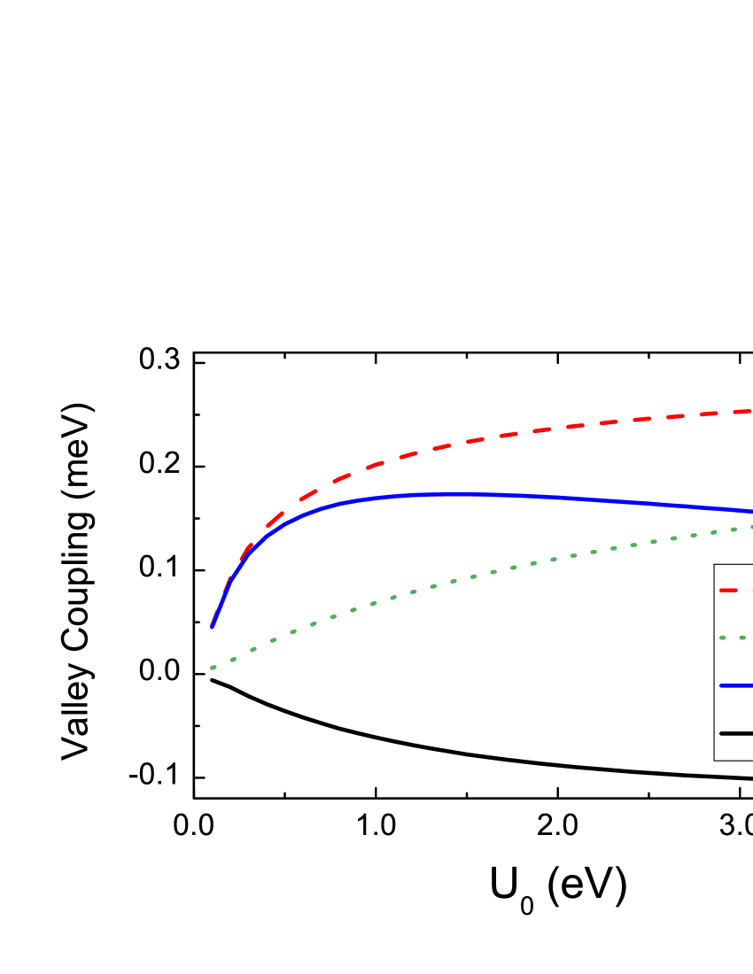
A richer behavior is obtained from , the contribution from the -function given in Eq. (8). Since this term is proportional to the product , there is a trade-off between the barrier height and the envelope function penetration into the barrier material. In Fig. 2 we note that increases with , meaning that, for V/nm, the increase in prevails over the reduction in .
Finally, the term arising from the evanescent tail contribution also presents a non-trivial trade-off. While some penetration of the envelope function into the barrier material is needed for this term to be non-vanishing, the integrand in equation (9) is highly oscillatory so that if the envelope function penetrates more than a few monolayers, integrates to zero. Since SiGe barriers present fairly large electronic penetration, the calculated for these materials is much smaller than in the case of SiO2 barriers. Besides, in the SiGe barrier the contribution only gives a change in the complex phase of , thus leading to . Still, since this small contribution to the intervalley coupling in Si/SiGe heterostructures changes its complex phase, it leads to a different ground state combination of the valleys.
III.3 Umklapp Processes
Since we take the plane wave expansion of both conduction band minima, Umklapp processes are fully included here. An estimate of their relevance is given by the total summation over them, which gives , while the contribution from is .
We also look at each plane wave contribution separately. The most prominent terms in the PW expansion of the Bloch functions at the conduction band minima are not the term, but the first nearest neighbors in the BCC reciprocal lattice, as can be seen in Table 1.
Table 2 shows the numerical prefactors, multiplying , of the contributions to the imaginary part, confirming that the most relevant contributions come from the point and its first eight neighbors in the BCC reciprocal lattice of Si since we get over 70% of the total value coming from these points. Notice the Umklapp terms are the most relevant.
It is also interesting to note that for the imaginary part the most relevant contributions are obtained for . This is equivalent to taking the zeroth order plane wave expansion of the product , a commonly adopted approximation in the EMA theory of shallow donors. Debernardi et al. (2006) But a complete analysis of the Umklapp processes reveals that this is particular to the delta contribution, and that there is no general justification for this approximation for the interface induced valley coupling.
| Contribution | ||
|---|---|---|
| -0.01108 | ||
| 0.00410 | ||
| 0.00410 | ||
| 0.00410 | ||
| 0.00410 | ||
| 0.00410 | ||
| 0.00410 | ||
| 0.00410 | ||
| 0.00410 |
III.4 Complete Valley Coupling
The absolute values, and , of the two terms contributing to and are shown as a function of the barrier height in Fig. 2. It is clear here that in general the two terms have different behaviors, and that they both give important contributions to the total coupling. However, for estimating the valley splitting, is a reasonable approximation for small barriers, such as those in Si/SiGe heterostructures. Noting that , we infer that is in general a complex number, not a purely imaginary quantity Saraiva et al. (2009). Since is purely imaginary, this triangle inequality is only true if has a non-vanishing real part. For instance, at eV, we have an intervalley coupling of meV. Also, and increase monotonically with , while decreases at large offsets. This indicates that the relative phase between and changes with .
In principle, SiGe and SiO2 barriers could lead to similar intervalley couplings. Of course these two materials present very different interface morphologies and are grown with different techniques, which should lead to differences between the intervalley couplings measured in each design. There has been reports of significantly different valley splitting even for the two interfaces of the same quantum well. Takashina et al. (2004)
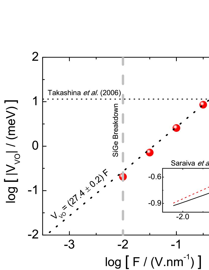
The valley coupling calculated for a range of external electric fields, covering several orders of magnitude are summarized in Fig. 3. This range expands by two orders of magnitude the previously reported range in Ref. Saraiva et al., 2009 (see inset). We take the upper limit of just below the SiO2 breakdown field V/nm. This bound is indicated in the figure, as well as the SiGe breakdown field V/nm. The lower value of is constrained by our numerical accuracy, as discussed in Sec. III.1. For large enough values of F, the valley splitting can be of the order of 10 meV, which is compatible (within error) with the giant splitting observed by Takashina et al. Takashina et al. (2006) This means that the results obtained in a SIMOX interface could be related to nearly perfectly sharp interfaces combined with relatively high gate fields, which might be consistent with the experimental conditions in terms of these two parameters. Other effects may be present that can further enhance this coupling and account for or contribute to very large splittings, as the recently proposed mechanism involving interface states. Saraiva et al. (2010)
Previous studies Sham and Nakayama (1979); Friesen et al. (2007) also report a linear dependence , where is a model-dependent length. This behavior in different models is qualitatively and quantitatively addressed in Sec. IV.
.
IV Discussions and Connections with previous model calculations
The problem of interface-induced intervalley coupling has been treated extensively in the literature, particularly within EMA. Since the complete problem is not exactly solvable, several approximations regarding the barrier potential and the nature of the electronic states have been adopted in different contexts. We discuss in this Section connections between our study and some previous contributions.
IV.1 Electric Field Dependence of the Valley Splitting
The applied field is one of the key parameters affecting , and probably the most controllable. Early work by Sham and Nakayama Sham and Nakayama (1979) established a linear dependence of the valley splittting on . They address the Si valley splitting problem from the perspective of the electrons in a space-charge layer in a MOSFET. The effect of the Si-SiO2 interface on electron dynamics is studied by considering incoming (towards the interface) and outgoing (away from the interface) Bloch waves in the Si region and evanescent waves decaying from the barrier inside the semiconductor. The potential barrier is modeled to be infinite, which disregards the evanescent tail of the electronic wavefunction into the barrier. Also, their study is devoted to the case of a planar density of electrons at the interface (of the order of cm-2 electrons), including many body corrections. In contrast, we develop here a theory for a single electron in a bound state, relevant in the context of quantum computing. Therefore, any comparison with Ref. Sham and Nakayama, 1979 should be taken with caution.
The valley splitting obtained by Sham and Nakayama, Sham and Nakayama (1979)
| (17) |
is proportional to the mean value of the derivative of the self-consistent potential. The parameter , a characteristic length related to the intervalley scattering matrix, is given as a function of the interface position with respect to a crystal (001) plane, (called there), showing sharp variations as runs over a 1 ML range. But the concept of an interface as an abrupt change in conduction band energy is not well defined in this scale. This ambiguity comes from the continuum EMA approach combined with the atomistic band structure input. These same ingredients affect our results, with the calculated valley coupling oscillating as a function of . Saraiva et al. (2009) We estimate that the mean value of the derivative of the self-consistent potential should be of the order of the field, , and take Å as estimated in Ref. Sham and Nakayama, 1979. Therefore Å.
More recent EMA-based models Friesen et al. (2006, 2007); Goswami et al. (2007); Chutia et al. (2008); Friesen and Coppersmith (2010) rely on an effective coupling potential responsible for the intervalley coupling, where the perturbation potential is taken as a -function with strength obtained from either TB atomistic calculations or experimental data. In our formalism, it means taking in equation (11) only the term . As discussed in the previous section and shown in Fig. 2, this approximation is better for the relatively low SiGe barriers, but for barrier materials with higher conduction band offsets, sizeable contributions (actually reducing ) come from the term. The valley couplings in Refs. Friesen et al., 2007 and Chutia et al., 2008 are also found to be linear with electric field, and their estimated values for are 0.72 Å and 1.36 Å respectively.
In our model calculations, the direct coupling () mediated by the field term in is found to be negligible. The effectiveness of comes from the electronic charge being pulled towards the barrier material, increasing the wavefunction amplitude at and beyond the interface position. These shifts contribute to the terms and in (11). From the linear fit of our data in Fig. 3, we get (present work)=27.4 mV/(V/nm) = 0.27Å, thus comparable to .111Fits to the results in Ref.Saraiva et al., 2009 (inset of Fig. 3) give Å or 0.12 Å for = 150 meV or 3 eV. For eV, the value Å, quoted here, is more reliable since it fits a wider range of fields, with data points obtained from a more accurate finite differences numerical solution. Results in Ref. Friesen et al., 2007 (alternatively, Ref. Chutia et al., 2008) are larger than by a factor of 3 (6), and are 2 (5) times larger than ours. Of course, there are many differences between the models which may account for the different results, but it is interesting to note from Fig. 2 that the delta-function term alone, , always overestimates the full coupling . Therefore, considering only the delta function potential in the coupling term may be related to larger values predicted for in Refs. Friesen et al., 2007 and Chutia et al., 2008.
The TB approach is also used to obtain more accurate boundary conditions at the interface for the EMA wavefunction. Chutia et al. (2008) Furthermore, the ambiguity introduced by the interface position discussed before was also recognized in this study, and explored in Ref. Friesen et al., 2007 to treat the interface position within the uncertainty range as a fitting parameter to match the TB and effective mass wavefunctions in a finite quantum well.
IV.2 Atomistic Approaches
More realistic quantitative estimates may be obtained from atomistic many band TB description of Si and the barrier material, Grosso et al. (1996); Boykin et al. (2004a, b); Friesen et al. (2006); Nestoklon et al. (2006); Lee and von Allmen (2006); Kharche et al. (2007); Boykin et al. (2008); Srinivasan et al. (2008) which may also account for interface disorder such as alloying effects and surface roughness. Such approaches are not always adequate or meant to give a general picture of the physical mechanisms behind the intervalley coupling, since the focus is to achieve quantitative accuracy. In some cases reasonable trade-off between atomistic description and analytical interpretations has emerged from simple one dimensional two band TB models. Boykin et al. (2004b, 2008)
Usually, the TB simulations are performed within a supercell approach, which involves periodic boundary conditions. So a Si/barrier interface is actually modeled by a finite-width Si slab surrounded laterally by two barriers, implying a quantum well arrangement if the barriers are wide enough (or superlattice for thin barriers). This introduces a width parameter to the Si slab which was shown to play an important role in the intervalley coupling, Grosso et al. (1996); Boykin et al. (2004a) except for high external electric fields and wide enough Si slabs, so that the electron interacts with a single interface. On the other hand, within EMA it is possible to pinpoint the role of a single interface, as both Si and the barrier material correspond geometrically to semi-infinite slabs.
Despite these differences, some TB studies give empirical evidence about the EMA analytical insights obtained here: (i) the linear behavior of the valley splitting with electric field, as discussed in Sec. IV.1; (ii) the relationship between the penetration of the wave-function in the barrier material and the barrier splitting explained in Sec. III and quantified by Eqs (8) and (9) was also empirically obtained by Srinivasan et al. Srinivasan et al. (2008) for Si electrostatic quantum dots embedded in SiGe buffers; (iii) finally the connection between the conduction band offset and the valley splitting demonstrated here in Fig. 2 similar to the TB study reported in Ref. Boykin et al., 2004b.
These examples illustrate how EMA studies may contribute to clarify the physics behind phenomena numerically obtained by more detailed atomistic approaches.
Other atomistic studies include ingredients that were not implemented in our formalism, such as magnetic field and interface disorder, so that it is not possible to quantitatively compare the results demonstrated within our general EMA study to those obtained within TB for particular systems/geometries.
IV.3 Low Field Dependence of the Valley Splitting
A non-linear dependence of with has been presented in TB studies by Grosso et al. Grosso et al. (1996) and Boykin et al. Boykin et al. (2004a) at low fields. We can not assess this behavior because of instabilities in our numerical procedure, mainly due to the size of the simulation cell required by the wavefunction spread at very low electric fields. It is possible that this nonlinear behavior is connected to the quantum well behavior at low , since the models in Refs. Grosso et al., 1996 and Boykin et al., 2004a refer to a quantum well, involving lengths associated with the Si well and the barriers widths, on which (particularly the Si well width) the TB results are quite sensitive. In all cases a linear behavior is obtained at larger values. The linear behavior is predicted in Ref.Sham and Nakayama, 1979 from Eq. (17), obtained there, with . It also emerges from a model for the variational envelope in a triangular-type potential with infinite barrier potential, simpler but still similar to Eq. (12), proposed by Fang-Howard Fang and Howard (1966) and generalized by Friesen et al. Friesen et al. (2007) to allow some penetration probability into the barrier region. In this case an analytic solution is obtained, and it can be shown that is proportional to the electric field, leading to linear increase of the intervalley coupling with . However, in most cases of interest the applied electric field should lead to a large enough , thus well within the linear regime ( V/nm here).
V summary and conclusions
We presented an EMA-based study of the valley splitting in Si induced by a Si/barrier interface. Our approach combines EMA with calculated Bloch functions, for which we give values of the relevant plane-wave expansion coefficients. The range of splittings we obtained are in fair agreement with measurements in Si/SiO2 and Si/SiGe interfaces. Takashina et al. (2006); Goswami et al. (2007) Our results for are comparable with experimentally measured values, indicating that we have probably included the most relevant physical ingredients in our model, as discussed in Ref. Saraiva et al., 2009 and expanded here. In particular, we show here that the puzzling values of the valley splittings obtained in Ref. Takashina et al., 2006 could result from particularly sharp interfaces in the very high electric field regime. We also confirm the linear dependence of the valley splitting on the electric field in this regime. Nonetheless, many effects contributing to the valley splitting are not included, such as strain, interface misorientation, Friesen et al. (2007) atomic scale disorder, Kharche et al. (2007) lateral confinement, Srinivasan et al. (2008) or many-body corrections Sham and Nakayama (1979); Friesen et al. (2007) and the recently proposed contribution from interface states. Saraiva et al. (2010)
It is important to reiterate here the double-focus of this paper : (i) to examine the effect of an applied electric field on the valley-orbit coupling at the interface, and (ii) to provide a clear interpretation of the physics of valley splitting. Understanding these points would hopefully reveal fundamental elements that affect the electron valley coupling and guide the identification of a suitable environment for electron spin qubits. By using the effective mass approximation we implicitly assume that the atomic configuration at the interface is not changed by the applied field (which should be a good approximation at low fields), and that interface roughness is small at the length scale over which the electron wave function changes significantly. Culcer et al. (2010b) A comprehensive study of valley splitting, including the effects of interface roughness, thickness, applied electric field, and other elements mentioned in the previous paragraph, would necessarily contain an atomistic component. Such a study would be required to clearly establish the limit of applicability of EMA, which is essentially a mean field approach for the bound electron wave function, interface disorder and composition profiles.
Our EMA approach provides a clear interpretation of the physics of valley splitting, revealing fundamental elements affecting the coupling and eventually providing a suitable environment for electronic spin qubit operation. While the investigation of other effects mentioned above is desirable, a simpler model that goes beyond the phenomenological approach, as provided here, is useful in guiding nanofabrication and device operation efforts. In particular, a profound understanding of the valley coupling induced by interfaces may pave the road to the quantum manipulation and processing of the valley degree of freedom. Culcer et al. (2011)
We also provide a critical analysis of the valley physics theory available in the literature, and discuss some of the ingredients that are imperative in a comprehensive theory. These include the correct interpretation of the valley coupling as a complex number and the inclusion of Umklapp processes.
In conclusion, we have calculated electron valley splitting in Si at a Si/barrier interface. We show that a sizeable single-particle valley-orbit coupling can be obtained by applying a high enough external field and choosing an optimal barrier material providing a suitable potential barrier height and high quality abrupt interface.
Acknowledgements.
We thank Mark Friesen, Kei Takashina and Yukinori Ono for helpful and fruitful discussions. This work was partially supported by the Brazilian agencies CNPq, FUJB, FAPERJ, and performed as part of the INCT on Quantum Information/MCT. MJC acknowledges FIS2009-08744 and the Ramón y Cajal program (MICINN, Spain). XH and SDS thank financial support by NSA and LPS through US ARO.References
- Das Sarma et al. (2004) S. Das Sarma, R. de Sousa, X. Hu, and B. Koiller, Solid State Commun. 133, 737 (2004).
- Rahman et al. (2009) R. Rahman, G. P. Lansbergen, S. H. Park, J. Verduijn, G. Klimeck, S. Rogge, and L. C. L. Hollenberg, Physical Review B 80 (2009).
- Culcer et al. (2010a) D. Culcer, L. Cywinski, Q. Z. Li, X. D. Hu, and S. Das Sarma, Physical Review B 82, 155312 (2010a).
- Culcer et al. (2010b) D. Culcer, X. D. Hu, and S. Das Sarma, Physical Review B 82, 205315 (2010b).
- Debernardi and Fanciulli (2010) A. Debernardi and M. Fanciulli, Physical Review B 81 (2010).
- Li et al. (2010) Q. Z. Li, L. Cywinski, D. Culcer, X. D. Hu, and S. Das Sarma, Physical Review B 81 (2010).
- Wang et al. (2010) L. Wang, K. Shen, B. Y. Sun, and M. W. Wu, Physical Review B 81 (2010).
- Koenraad and Flatte (2011) P. M. Koenraad and M. E. Flatte, Nature Materials 10, 91 (2011).
- Escott et al. (2010) C. C. Escott, F. A. Zwanenburg, and A. Morello, Nanotechnology 21 (2010).
- Rahman et al. (2011) R. Rahman, J. Verduijn, N. Kharche, G. P. Lansbergen, G. Klimeck, L. C. L. Hollenberg, and S. Rogge, Physical Review B 83 (2011).
- Raith et al. (2011) M. Raith, P. Stano, and J. Fabian, Physical Review B 83 (2011).
- Friesen et al. (2003) M. Friesen, P. Rugheimer, D. E. Savage, M. G. Legally, D. W. van der Weide, R. Joynt, and M. A. Eriksson, Phys. Rev. B 67, 121301 (2003).
- Eriksson et al. (2004) M. A. Eriksson, M. Friesen, S. N. Coppersmith, R. Joynt, L. J. Klein, K. Slinker, C. Tahan, P. M. Mooney, J. O. Chu, and S. J. Koester, Quantum Information Processing 3, 133 (2004).
- Kane (1998) B. E. Kane, Nature 393, 133 (1998).
- Kane (2000) B. E. Kane, Fortschr. Phys. 48, 1023 (2000).
- Ando et al. (1982) T. Ando, A. B. Fowler, and F. Stern, Rev. Mod. Phys. 54, 437 (1982).
- Kane et al. (2000) B. E. Kane, N. S. McAlpine, A. S. Dzurak, R. G. Clark, G. J. Milburn, H. B. Sun, and H. Wiseman, Phys. Rev. B 61, 2961 (2000).
- Herring and Vogt (1956) C. Herring and E. Vogt, Phys. Review 101, 944 (1956).
- Saraiva et al. (2009) A. L. Saraiva, M. J. Calderon, X. Hu, S. Das Sarma, and B. Koiller, Phys. Rev. B 80, 081305 (2009).
- Goswami et al. (2007) S. Goswami, K. A. Slinker, M. Friesen, L. M. McGuire, J. L. Truitt, C. Tahan, L. J. Klein, J. O. Chu, P. M. Mooney, D. W. van der Weide, et al., Nat. Phys. 3, 41 (2007).
- Takashina et al. (2006) K. Takashina, Y. Ono, A. Fujiwara, Y. Takahasho, and Y. Hirayama, Phys. Rev. Lett. 96, 236801 (2006).
- Loss and DiVincenzo (1998) D. Loss and D. P. DiVincenzo, Phys. Rev. A 57, 120 (1998).
- Ono et al. (2002) K. Ono, D. G. Austing, Y. Tokura, and S. Tarucha, Science 297, 1313 (2002).
- Culcer et al. (2009) D. Culcer, L. Cywinski, Q. Li, X. Hu, and S. D. Sarma, Phys. Rev. B 80, 205302 (2009).
- Ohkawa and Uemura (1977) F. J. Ohkawa and Y. Uemura, J. Phys. Soc. Jpn. 43, 907 (1977).
- Sham and Nakayama (1979) L. Sham and M. Nakayama, Phys. Rev. B 20, 734 (1979).
- Resta (1977) R. Resta, J. Phys. C: Solid State Phys. 10, L179 (pages 4) (1977).
- Ando et al. (1989) T. Ando, S. Wakahara, and H. Akera, Physical Review B 40, 11609 (1989).
- Ando and Akera (1989) T. Ando and H. Akera, Physical Review B 40, 11619 (1989).
- Ando (1995) T. Ando, Japanese Journal of Applied Physics 34, 4522 (1995).
- Menchero et al. (1999) J. G. Menchero, B. Koiller, and R. B. Capaz, Physical Review Letters 83, 2034 (1999).
- Hedin (1965) L. Hedin, Phys. Rev. 139, A796 (1965).
- Grosso et al. (1996) G. Grosso, G. P. Parravicini, and C. Piermarocchi, Phys. Rev. B 54, 16393 (1996).
- Boykin et al. (2004a) T. B. Boykin, G. Klimeck, M. A. Eriksson, M. Friesen, S. N. Coppersmith, P. von Allmen, F. Oyafuso, and S. Lee, Appl. Phys. Lett. 84, 115 (2004a).
- Boykin et al. (2004b) T. B. Boykin, G. Klimeck, M. Friesen, S. N. Coppersmith, P. von Allmen, F. Oyafuso, and S. Lee, Phys. Rev. B 70, 165325 (2004b).
- Friesen et al. (2006) M. Friesen, M. A. Eriksson, and S. N. Coppersmith, Appl. Phys. Lett. 89, 202106 (2006).
- Nestoklon et al. (2006) M. O. Nestoklon, L. E. Golub, and E. L. Ivchenko, Phys. Rev. B 73, 235334 (2006).
- Lee and von Allmen (2006) S. Lee and P. von Allmen, Phys. Rev. B 74, 245302 (2006).
- Kharche et al. (2007) N. Kharche, M. Prada, T. B. Boykin, and G. Klimeck, Appl. Phys. Lett. 90, 092109 (2007).
- Boykin et al. (2008) T. B. Boykin, N. Kharche, and G. Klimeck, Phys. Rev. B 77, 245320 (2008).
- Srinivasan et al. (2008) S. Srinivasan, G. Klimeck, and L. P. Rokhinson, Appl. Phys. Lett. 93, 112102 (2008).
- Bastard (1988) G. Bastard, Wave mechanics applied to semiconductor heterostructures (Halsted, New York, 1988).
- Helms and Poindexter (1994) C. R. Helms and E. H. Poindexter, Reports on Progress in Physics 57, 791 (1994).
- Ramos et al. (2004) L. Ramos, J. Furthmuller, and F. Bechstedt, Phys. Rev. B 69, 085102 (2004).
- Rieger and Vogl (1993) M. M. Rieger and P. Vogl, Phys. Rev. B 48, 14276 (1993).
- Takahashi et al. (1999) Y. Takahashi, A. Fujiwara, M. Nagase, H. Namatsu, K. Kurihara, K. Iwadate, and K. Murase, Int. J. Electronics 86, 605 (1999).
- Kohn (1957) W. Kohn, Solid State Physics Series, vol. 5 (Academic Press, 1957), edited by F. Seitz and D. Turnbull.
- Koiller et al. (2004) B. Koiller, R. B. Capaz, X. Hu, and S. Das Sarma, Phys. Rev. B 70, 115207 (2004).
- Gonze et al. (2002) X. Gonze, J.-M. Beuken, R. Caracas, F. Detraux, M. Fuchs, G.-M. Rignanese, L. Sindic, M. Verstraete, G. Zerah, F. Jollet, et al., Computational Materials Science 25 (2002), (URL http://www.abinit.org).
- Hohenberg and Kohn (1964) P. Hohenberg and W. Kohn, Phys. Rev. 136, 84B (1964).
- Kohn and Sham (1965) W. Kohn and L. J. Sham, Phys. Rev. 140, 1133A (1965).
- Perdew and Zunger (1981) J. P. Perdew and A. Zunger, Phys. Rev. B 23, 5048 (1981).
- Ceperley and Alder (1980) D. M. Ceperley and B. J. Alder, Phys. Rev. Lett, 45, 566 (1980).
- Troullier and Martins (1991) N. Troullier and J. L. Martins, Phys. Rev. B 43, 1993 (1991).
- Fuchs and Scheffler (1999) M. Fuchs and M. Scheffler, Comput. Phys. Commun. 119, 67 (1999).
- Madelung (1996) O. Madelung, Semiconductors-Basic Data (Springer, Berlin, 1996).
- Stern (1972) F. Stern, Phys. Rev. B 5, 4891 (1972).
- Debernardi et al. (2006) A. Debernardi, A. Baldereschi, and M. Fanciulli, Phys. Rev. B 74, 035202 (2006).
- Takashina et al. (2004) K. Takashina, A. Fujiwara, S. Horiguchi, Y. Takahashi, and Y. Hirayama, Phys. Rev. B 69, 161304 (2004).
- Saraiva et al. (2010) A. L. Saraiva, B. Koiller, and M. Friesen, Phys. Rev. B 82, 245314 (2010).
- Friesen et al. (2007) M. Friesen, S. Chutia, C. Tahan, and S. N. Coppersmith, Phys. Rev. B 75, 115318 (2007).
- Chutia et al. (2008) S. Chutia, S. N. Coppersmith, and M. Friesen, Phys. Rev. B 77, 193311 (2008).
- Friesen and Coppersmith (2010) M. Friesen and S. N. Coppersmith, Phys. Rev. B 81, 115324 (2010).
- Fang and Howard (1966) F. F. Fang and W. E. Howard, Phys. Rev. Lett. 16, 797 (1966).
- Culcer et al. (2011) D. Culcer, A. L. Saraiva, B. Koiller, X. Hu, and S. Das Sarma, arXiv:1107.0003v1 (2011).