Characterisation of
a CMOS Active Pixel Sensor
for use in the TEAM Microscope
Abstract
A 1M- and a 4M-pixel monolithic CMOS active pixel sensor with 9.59.5 m2 pixels have been developed for direct imaging in transmission electron microscopy as part of the TEAM project. We present the design and a full characterisation of the detector. Data collected with electron beams at various energies of interest in electron microscopy are used to determine the detector response. Data are compared to predictions of simulation. The line spread function measured with 80 keV and 300 keV electrons is (12.1 0.7) m and (7.4 0.6) m, respectively, in good agreement with our simulation. We measure the detection quantum efficiency to be 0.780.04 at 80 keV and 0.740.03 at 300 keV. Using a new imaging technique, based on single electron reconstruction, the line spread function for 80 keV and 300 keV electrons becomes (6.7 0.3) m and (2.4 0.2) m, respectively. The radiation tolerance of the pixels has been tested up to 5 Mrad and the detector is still functional with a decrease of dynamic range by 30 %, corresponding to a reduction in full-well depth from 39 to 27 primary 300 keV electrons, due to leakage current increase, but identical line spread function performance.
keywords:
Monolithic active pixel sensor, Transmission Electron Microscopy, Point Spread Function, Detection Quantum Efficiency;, , , , , , , ,
1 Introduction
The TEAM (Transmission Electron Aberration-corrected Microscope) Project [1] has developed the most powerful electron microscope to date, with unprecedented sensitivity and spatial resolution, 50 pm [2] in both TEM (Transmission Electron Microscopy) and Scanning TEM (STEM). This was accomplished through advances in electron optics, particularly aberration correction, and the TEAM project included the development of new kinds of specimen stages and detectors.
One of the goals of the TEAM project is to be able to observe the dynamics of processes at the atomic scale [3, 4], which requires advances over conventional TEM detectors. These include film, image plates and phosphors fiber-coupled to CCDs. Each of these techniques has fundamental limitations for high-speed in-situ imaging. Film and image plates directly detect electrons with high spatial granularity but require relatively long exposures and are obviously not high-speed. Phosphors fiber-coupled to CCDs have a modest time granularity but are limited in their point spread function (PSF) and detection quantum efficiency (DQE) due to the physics limitations of the steps needed to convert the primary electrons into charge on the CCD cell. A high-speed detector able to directly detect electrons appears an ideal solution for TEM imaging. The key requirements for TEAM are a minimum of 1k 1k pixels, in order to obtain a field of view of 200 Angstrom with a magnified pixel size of 3 pixels/0.5 Angstrom (provided the PSF is 1 pixel) and a readout time of 10 ms, providing 100 or more frames/s. As TEAM is designed for material science applications, suitable radiation hardness is essential. Considering the standard way of operation of experiments in TEM, a radiation tolerance of 1 Mrad would enable its use for approximately one year, which appears to be a valid requirement.
There has been significant interest in the application of both CMOS [7, 8, 9] and hybrid [10, 11, 12] pixel sensors for direct imaging in TEM, to replace conventional CCDs optically-coupled to phosphor plates [13]. In two recent papers [14, 15] in this journal we discussed the design of a CMOS sensor prototype with a radiation-hard pixel cell and characterised its response in terms of energy deposition and line spread function. We found that by proper design of the pixel cell the sensor can be made enough radiation tolerant to operate properly up to several Mrad of ionising dose and the line spread function for 10 m pixel varies from 12 m to 8 m for electrons in the energy range 80 keV 300 keV of interest in TEM. These results motivated the development of a larger size pixel chip to perform tests of fast imaging at TEAM. The final TEAM detector contains 2k 2k pixels with 100 frames/s readout. As an intermediate stage, 1k 1k detectors were fabricated. In this paper we present the design of the TEAM1k pixel chip and discuss the results of its characterisation on a TEAM project test column.
2 The TEAM Pixel Sensors
The TEAM1k and TEAM2k detectors are fabricated in a 0.35 m CMOS process. For the TEAM1k, four 1 1 cm2 chips are placed within the 2 2 cm2 reticle area and for the TEAM2k the entire reticle is used. All chips employ an identical 9.5 9.5 m2 pixel. In the TEAM1k reticle, two of the chips have a 1,0241,024 pixel imaging area (“imaging” version), and the other two chips have the same imaging area, except that a central 500 m circular area is replaced with a simple diode (“diffraction” version). One “imaging” and one “diffraction” chip are designed with analog and digital sections very similar to the design previously reported, as backup designs. The other two “imaging” and “diffraction” chips have several improvements over previous designs, and these new versions are the ones discussed in this paper. The TEAM1k chips are organised as 16 identical slices each with 1,024 rows and 64 columns. Each slice has a novel analog output buffer, capable of driving a capacitive load of up to 20 pF. In addition, each slice has a variable bottom-of-column current load, which can “look ahead” a programmable number of columns. In a conventional active pixel sensors (APS), there is a fixed current bias at the bottom of the column. In order to reduce power, as the sensor has to be operated in vacuum, the standing current in this bias should be small. For speed, though, this current needs to be large enough for the signal to slew within the time needed to digitise a pixel. In this implementation, a larger bias current is switched on when the given column is selected (), and clock cycles before () and then maintained for the next clock cycle when the column is selected. Sending the output to digitising electronics outside of the microscope vacuum requires an amplifier capable of providing high currents as needed to drive the capacitive load. Again, with the desire to minimise power, the output stage consists of two parts: a conventional low-power operational amplifier, along with a higher-power slew rate enhancer (SRE). The small-signal amplifier has the necessary gain, bandwidth, and noise performance to settle to the required precision, while the SRE minimises the fraction of the sample period that is spent slewing a large voltage step. The SRE is activated when the error voltage at the small-signal amplifier input exceeds a designed value.
Since charge generation is confined primarily to the thin epitaxial layer, just 14 m thick, it is possible to remove most of the underlying detector bulk silicon using a back-thinning process. The charge collection, noise and charge-to-voltage calibration have been studied by characterising a batch of CMOS pixel sensors before and after back-thinning and no significant effects have been observed [16]. Back-thinning is performed by Aptek Industries [17] using a proprietary technique. The process has been extensively tested and yields in excess of 90 % have been obtained for thicknesses down to 50 m [16]. TEAM1k detectors are thinned to 50 m. The use of thin sensors minimises the charge spread due to back-scattering in the bulk, thus maximising the contrast ratio in TEM imaging.
3 Response Simulation
The energy deposition in the sensor active layer and the lateral charge spread are simulated with the Geant4 program [18], using the low-energy electromagnetic physics models [19]. The CMOS pixel sensor is modelled according to the detailed geometric structure of oxide, metal interconnect and silicon layers, as specified by the foundry. Electrons are incident perpendicular to the detector plane and tracked through the sensor. For each interaction within the epitaxial layer, the energy released and the position are recorded.
Charge collection is simulated with PixelSim, a dedicated digitisation module [20], developed in the Marlin C++ reconstruction framework [21] as discussed in [14]. The simulation has a single free parameter, the diffusion constant , used to determine the width of the charge carrier cloud. Its value is extracted from data by a fit to the pixel multiplicity in the clusters obtained for 300 keV electrons. We find = (14.5) m, which is compatible with both the value obtained for 1.5 GeV s with a prototype having 2020 m2 pixels produced in the same CMOS process [15] and that inferred from the diffusion length (estimated from the doping in the epitaxial layer) and the measured charge collection time [14].
4 Sensor Tests
The sensor response to ionising radiation is studied with 5.9 keV X-rays and electrons of energy ranging from 80 keV to 300 keV. The microscope tests are carried out in the FEI Titan test column at the National Center for Electron Microscopy (NCEM). The prototype chip is mounted on a proximity board which is held on the film insertion plate of the microscope. The insertion plate is built on a removable mechanical assembly which allows easy and quick replacement of the sensor. The plate can be inserted in and retracted from the column by means of a pneumatic actuator.
The temperature is monitored during operation by measuring the resistance of a temperature-sensitive resistor included in the chip. In absence of active cooling, the thick sensor operates at a temperature of 90 ∘C, while the thin sensor between 40 and 50 ∘C, depending on running conditions. Data are taken for 6.25 and 25 MHz clock frequency and different beam intensities. For response characterisation, four contiguous sectors of the chip are tested at the same time, the four analog outputs being read out in parallel. Two flex cables, exiting from the column through a vacuum feed-through, provide the interconnection with the data acquisition and monitoring electronics located outside the microscope. An intermediate board provides the chip with the biases and driving clocks, performs signal amplification and deploys differential stages for adapting the analog output signals to the data acquisition (DAQ) system.
4.1 Data Acquisition and Analysis
For this study a custom DAQ system [22] is used. Data from four of the chip analog outputs are digitised by four 100 MS/s, 14-bit ADCs on a custom-designed board interconnected with a commercial development board [23], implementing a Xilinx Virtex-5 FPGA device, 64 Mb of on-board DDRAM memory and communication devices. Clock pattern generation and chip control is performed via high-speed LVDS lines by the Virtex-5, which also controls and synchronises the acquisition with the ADCs reference clock.
The DAQ system is connected to a control PC via a USB 2.0 bus, for acquisition control and DAQ steering through dedicated registers and for data retrieval. The bandwidth for data transfer is 40 Mbytes/s. A graphical user interface based on a series of dedicated C/C++ classes interfaced to the ROOT [24] framework classes provides an intuitive and easy-to-use system for acquisition monitoring, fast data display and on-line processing [22]. Raw data is stored in ROOT format, and further converted in the LCIO [25] format for offline analysis. This is performed with a set of dedicated processors, developed in the Marlin reconstruction framework.
4.2 Noise, Uniformity and Calibration
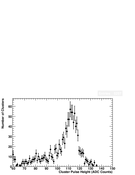
The sensor noise and uniformity among the different analog outputs are measured in the lab in dark. The pedestal level for each pixel is computed from the average pulse height over 100 consecutive acquisitions. A pixel-to-pixel dispersion of less than 8 mV is obtained. The pedestal dispersion varies within 2% among the different analog outputs of the same sensor. An average pixel leakage current below 10 fA is inferred from the results of measurements performed at different clock frequencies ranging from 25 MHz down to 6.25 MHz, corresponding to integration times of 2.6 ms and 10.5 ms, respectively. The sensor charge-to-voltage conversion gain is measured from the response to 5.9 keV X-rays from a 55Fe source, corresponding to a charge generation of 1640 electrons. Figure 1 shows the spectrum obtained on one analog output for a clock frequency of 6.25 MHz, at room temperature. A calibration of 14.9 e-/ADC count is obtained. The gain of the different analog outputs of the same sensor is found to vary within 3%. The charge-to-voltage conversion gain is expected to depend on the voltage applied to the pixel diode junction. For small signals, as those induced by one or few electrons, the capacitance of the junction can be considered constant and the conversion linear. For larger signals obtained when many electrons hit the same pixel in a single frame the capacitance of the diode junctions is expected to increase by several percent, up to 20% for signals corresponding to the full sensor dynamic range. Since most of the analyses reported in this paper deal with relatively small signals, up to few tens of electrons or less, we assume a constant calibration factor in the analysis. Typical average pixel noise figures of (322) e- and (282) e- of equivalent noise charge (ENC) are measured under operating condition in the microscope set-up for clock frequencies of 25 and 6.25 MHz, respectively.
4.3 Electron Response
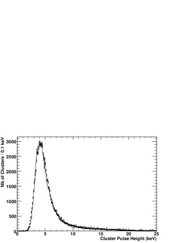
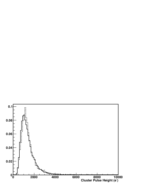
The response to single electrons is characterised in terms of energy deposition and cluster size. We study the energy deposition in the sensor pixels, varying the number of electrons recorded per pixel and per frame. First, we operate with a flux of 50 mm-2 frame-1, which allows us to resolve individual electrons. Under these conditions, electron hits are reconstructed as pixel clusters. For these events the sensor response is characterised in terms of the number of pixels associated to a cluster and the pulse height measured in a 55 pixel matrix centred around a seed pixel. The response measured on data is compared to the Geant4+PixelSim simulation. Figure 2 shows the reconstructed energy deposited by 300 keV electrons for data and simulation. A good agreement is observed.
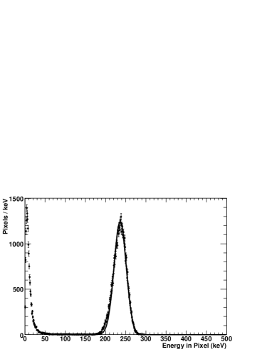
The uniformity across a detector sector has been studied for bright field illumination at a flux corresponding to an energy deposition of 200 keV pixel-1 frame-1. The distribution of the energy recorded in each pixel in a single frame is shown in the right panel of Figure 2. The dispersion of signal on the pixels fully exposed to the electron beam is obtained by a Gaussian fit to the recorded energy distribution. The relative r.m.s. dispersion at 300, 200, 120 and 80 keV is 0.063, 0.058, 0.080 and 0.11, respectively. The increase at lower energies is interpreted as an effect of the larger energy loss fluctuations, since measurements are performed at constant energy per pixel instead of constant number of electrons per pixel.
 |
 |
 |
 |
 |
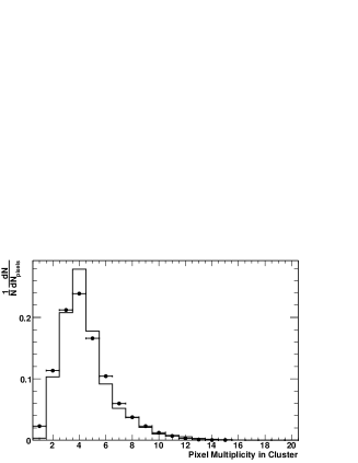 |
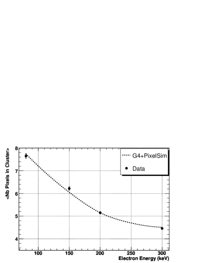
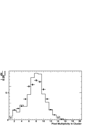
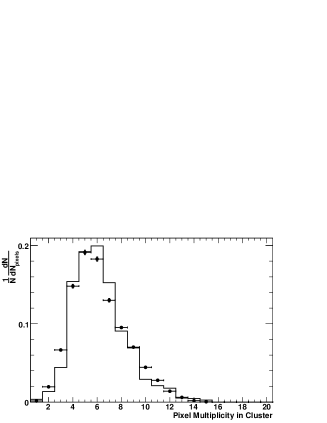
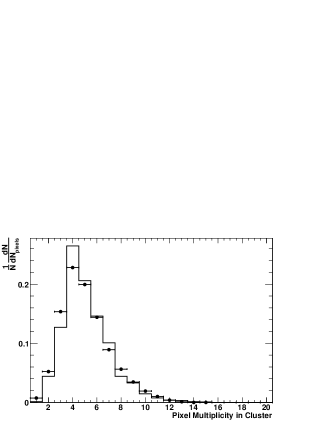
The study of the cluster size allows us to investigate the charge spread around the point of impact of each electron onto the detector. This is used to validate the simulation and to assess the variation of the charge spread as a function of the electron energy. A clustering algorithm with two thresholds is used to determine the cluster size [14]. First the detector is scanned for “seed” pixels with pulse height values over a S/N threshold set to 3.5. Seeds are sorted according to their pulse heights and the surrounding neighbouring pixels are added to the cluster if their S/N exceeds 2.5. In simulation, the parameter is tuned to minimise the of the pixel multiplicity distribution in the clusters for simulation vs. data at 300 keV, where multiple scattering is lower, as discussed above. The pixel multiplicities in electron clusters at various energies are shown in Figure 3 and the evolution of the average pixel multiplicity vs. electron energy in Figure 4. The agreement of the tuned PixelSim simulation with data is good and we observe an increase of the pixel multiplicity due to the increased multiple scattering and energy deposition at lower energies.
5 Imaging Characterisation
The pixel imaging performance is characterised in terms of three observables: the line spread function (LSF), the modulation transfer function (MTF) and the detection quantum efficiency (DQE). We study these observables for two different imaging regimes, bright field illumination, where each pixel typically receives several electrons per frame, and for cluster imaging, a recently proposed alternative imaging technique [26], where the electron flux is kept low enough that the position of impact of each individual electron is reconstructed by interpolating the charge collected on the pixels of a signal cluster. This allows us to achieve spatial sampling with frequencies much larger than the Nyqvist frequency.
The point spread function is one of the key features for an imaging sensor in transmission electron microscopy. It depends on several parameters of which the most important are pixel size, electron multiple scattering in the active layer and in its vicinity and charge carrier diffusion. For these tests the detector is mounted on a proximity board which is cut below its active area to eliminate back-scattering from the board material. Pixel sensors of both 300 m- and 50 m-thickness are tested. A 60 m-diameter Au wire is mounted parallel to the pixel rows on top of each sensor at a distance of 2 mm above its surface.
Another important feature is the image contrast, defined by the ratio between the signal on the pixels directly exposed to the beam to the response of those which are covered. The contrast depends on charge leakage, scattering and noise. We measure it using both the wire and a metal foil covering the upper portion of the chip. We expect the contrast to improve for thin sensors, where the contribution of electrons back-scattered in the the bulk Si and depositing energy in the shadowed area is smaller.
5.1 Bright Field Illumination
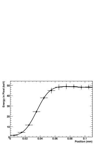
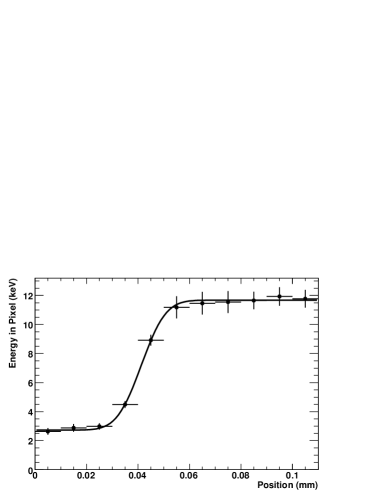
In simulation, a monochromatic, point-like beam of electrons is sent onto the surface of the detector. The line spread function (LSF) is determined as the r.m.s. of the predicted distribution of the detected charge on the pixels. On the data the LSF for bright field illumination is determined using the image projected onto the sensor by the thin Au wire, using the same technique as in [14]. Since the gold wire has well-defined edges, the profile of the deposited energy in the pixels, measured across the wire, allows us to study the charge spread due to scattering and diffusion along the projected image of the wire edge and compare to simulation. We study the change in the recorded signal, by scanning along pixel rows across the gold wire. We extract the LSF from images such as those in Figure 5, which show the pulse heights measured on the pixels along a set of rows. In [14], we parametrised the measured pulse height on pixel rows across the wire image with a box function smeared by a LSF Gaussian term and extracted the LSF by a 1-parameter fit with the Gaussian width as free parameter. Here we adopt an extension of this method which uses the sum of several sigmoid functions to describe the edge as proposed in [27]:
| (1) |
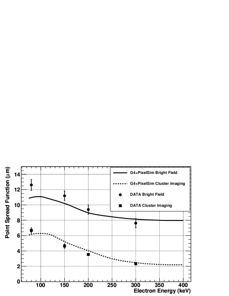
where the error function is defined as . We find that one or two sigmoid functions are sufficient to describe the data. We use a single sigmoid function to obtain LSF values of (7.60.6) m at 300 keV and (12.60.7) m at 80 keV, where the quoted uncertainty is statistical. These results are consistent with those obtained from simulation and with the data in our previous study.
 |
 |
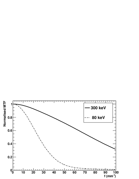
Since it is customary to quote the imaging resolution in terms of the modulation transfer function (MTF), which is the Fourier transform of the line spread function, we repeat the fit using the sum of two sigmoid functions in Eq 1.
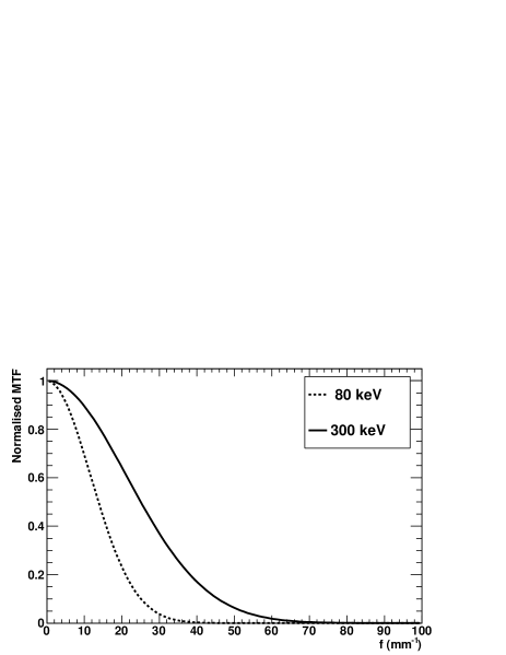
The width of the first, , is fixed to its value obtained in the previous fit, using a single function, while the width of the second function, , as well as the two normalisation coefficients and are left free. We observe that the at the minimum improves only marginally by performing the fit with two functions compared to a single function, as used to extract the LSF. Figure 6 shows the MTF obtained with this method on data, for 80 keV and 300 keV electrons.
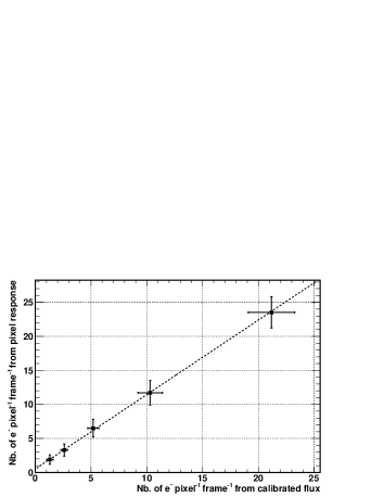
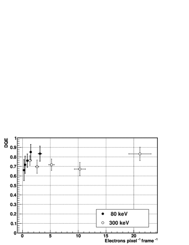
Next we determine the detection quantum efficiency, a quantity widely used to characterise electron detection systems, introduced in [28]. We compute the DQE accounting for the charge migration between neighbouring pixels due to charge carrier diffusion following the method adopted in [29, 30]:
| (2) |
where is the number of electrons pixel-1 frame-1 and is the mixing factor, given by , with being the fraction of the charge collected at pixel for an electron hitting the detector on pixel . We extract the coefficients by studying the charge distribution in the signal clusters for single electrons, as discussed in section 4.3. We perform this measurement varying the electron flux and measuring the current on the calibrated phosphor screen of the Titan microscope. We take data at different fluxes in the range 1.3 to 21 e- pixel-1 frame-1 at 300 keV and 0.3 to 3.1 e- pixel-1 frame-1 at 80 keV. First, we determine the number of electrons per pixel and per frame from the pixel single electron response in terms of pulse height and charge spread, discussed in section 4.3. The left panel of Figure 7 shows the number of electrons per pixel and frame measured from the pixel response as a function of that from the beam current on the phosphor screen, which exhibits a linearity within 10 %.
 |
 |
5.2 Cluster Imaging
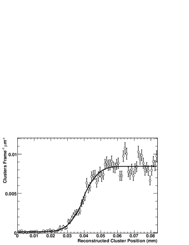
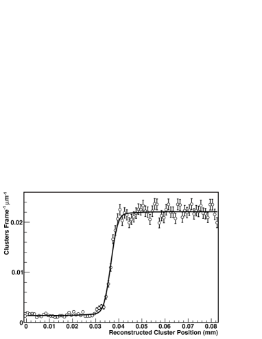
In bright field illumination the point spread function has a contribution from the lateral charge spread due to charge carrier diffusion in the active detector volume. At high rate, the signal recorded on each individual pixel is the superposition of the charge directly deposited by a particle below the pixel area with that collected from nearby pixels through diffusion, multiple scattering and back-scattering from the bulk Si. If the electron rate is kept low enough so that individual electron clusters can be reconstructed, the position of passage of each electron can be obtained from the centre of gravity of the observed signal charge. The leakage of charge on neighbouring pixels is taken into account through the centre of gravity calculation and the precision depends on the signal-to-noise ratio. This technique, widely adopted in tracking applications for accelerator particle physics, provides us with a significant gain in spatial resolution. In a recent letter to this journal [26] we proposed to adopt the same technique for imaging, with low electron fluxes, i.e. 102 e- mm-2 frame-1. We named this technique “cluster imaging”. In this regime, the image is formed by adding many subsequent frames. We showed that for cluster imaging the LSF depends only on the detector pixel size and cluster S/N (determining the single point resolution) and on the multiple scattering. A significant improvement in the LSF can be obtained.
 |
 |
| Electron | Bright Field | Cluster Imaging |
|---|---|---|
| Energy | LSF | LSF |
| (keV) | (m) | (m) |
| 80 | 12.10.7 | 6.680.34 |
| 150 | 11.20.6 | 4.640.27 |
| 200 | 9.40.6 | 3.530.16 |
| 300 | 7.40.6 | 2.350.15 |
Here, we repeat the analysis by extracting the LSF from the wire edge images built by the superposition of multiple frames taken with 10-40 e- mm-2 frame-1, using the same sigmoid fit adopted above.
First we use a single sigmoid to extract the value of the LSF. Results are summarised in Table 1 and Figure 9, where the values for bright field illumination and cluster imaging measured at different energies are compared. Then, we fix the width of the first function to this fitted value and we introduce a second sigmoid with free width and fit it together with the normalisation coefficients, as discussed above. The LSF function, parametrised according to Eq. (1), is used to extract the MTF. Results are shown in Figure 10 for 300 keV and 80 keV electrons.
5.3 Image Contrast and Imaging Tests
We study the contrast ratio obtained for a 50 m-thick sensor and a sensor which has the original 300 m Si thickness, by comparing the signal observed on the pixel area covered by the wire to that obtained on the pixels directly exposed to the beam. We measure a ratio of 2.95 for the 300 m-thick and 4.49 for the 50 m-thick sensor, using bright field illumination.
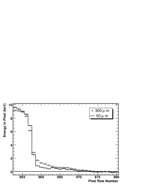
The contrast is affected by multiple scattering effects in the detector and the thinned sensor performs better due to the reduced back-scattering in the bulk Si underneath the sensitive epitaxial layer. The contrast decreases at lower energies, we measure 3.9 on the thin sensor at 150 keV, until the range of the electrons becomes short enough that the scattering contribution to the energy leaking under the shadow of the wire becomes small and a contrast ratio in excess of 20 is measured at 80 keV. Then, we study the pixel response at the edge of a metal plate on the thick and the thinned sensor. The plate covers an area where pixels do not receive direct electron hits. Figure 11 shows the pulse height measured on pixels along rows across the plate edge. Beyond the sharp edge we observe that the recorded signal in the thick sensor falls less rapidly compared to that in the thin sensor, which we interpret as an effect of charge deposited by back-scattered electrons. We also measure the LSF by fitting a single sigmoid function to the pixel response. We obtain (10.40.5) m and (7.70.4) m for the 300 m- and the 50 m-thick sensor, respectively. The latter result is compatible to that obtained with the thin Au wire.
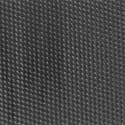
Finally, we perform an imaging test using a Si sample on the TEAM1 microscope with 300 keV electrons. Figure 12 gives a qualitative demonstration of the performance of the TEAM1k detector. The image shows a single 2.6 ms exposure revealing the Si dumbbells close to the zone axis, with a spacing of 1.36 Angstrom.
6 Sensor irradiation
The radiation tolerance of the chip has been assessed by irradiating a TEAM1k sensor with 300 keV electrons, up to a dose of 5 Mrad. The damage mechanism is an increase of leakage current, which not only increases noise, but also decreases the dynamic range. CMOS active pixel sensors are capable of good S/N because the charge collection node capacitance is small, resulting in a high conversion gain (V/) and thus high sensitivity to leakage current. The irradiation has been performed in subsequent steps with a flux of 875 sm-2, corresponding to a dose rate of 250 rad s-1, from the measured beam current on a known beam spot area onto the Titan calibrated phosphor screen. In-between consecutive irradiation steps, several dark frames are acquired without beam, in order to follow the evolution of the pixel leakage current with the dose, and with very low intensity beam, to monitor the pixel response to single electrons and the gain calibration. A small portion of the sensor active surface is covered with a gold wire, as described in Section 5. Bright field images of this wire are acquired throughout the irradiation in order to monitor also the sensor imaging performance. All tests are performed with the detector cooled at +5∘C. The sensor is glued with thermally conductive epoxy to an AlN substrate board, and wire-bonded to a flex circuit glued on top of the AlN board. Heat is removed from the sensor by a copper finger that contacts the AlN board and is cooled by a double-Peltier system.
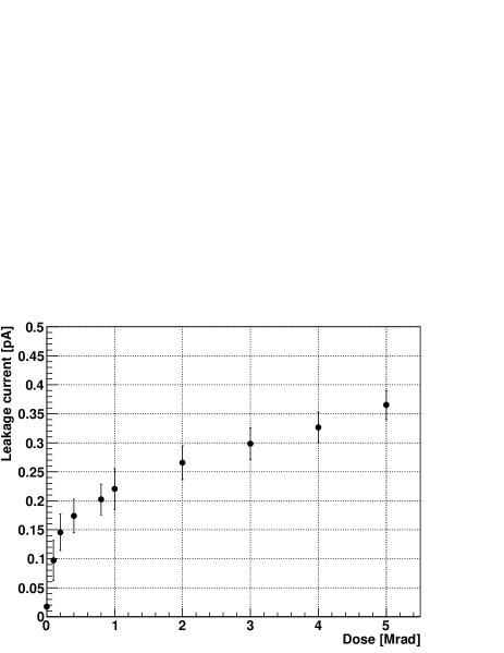
Figure 13 shows the evolution of the pixel leakage current with dose. The leakage current is determined by comparing the pixel base level at two different clock frequencies, 25 MHz and 6.25 MHz, corresponding to integration times of 2.6 ms and 10.5 ms, respectively. A sub-linear increase of the current with dose is observed, reaching about 0.4 pA after 5 Mrad. The leakage current increase is due to ionising damage in the field oxide that leads to trapping of positive charge. The inversion of the Si interface results in an increased current in the charge collecting diode. 300 keV electrons are not expected to significantly affect the silicon bulk through displacement damage.
Results of the irradiation test of an earlier prototype chip with a comparable pixel cell manufactured in the same process gave a leakage current of 0.2 pA after a dose of 1.11 Mrad with 200 keV electrons on 2020 m2 pixels. The test was performed at room temperature and for an integration time of 737 s. Considering that the integration time of the TEAM1k chip is 14 times longer, the beneficial effect of cooling on the sensor radiation tolerance is evident.
From a device operation point of view, the increase of the leakage current results in an increase of the pixel base level. This is removed by subtraction of the pedestal level. However, the leakage current increase causes a decrease of the dynamic range and an increase of the single pixel noise. At 25 MHz clock frequency, after 5 Mrad of dose we observe a decrease of the pixel dynamic range by about 30%, which still allows proper operation of the chip.
| Dose | Calibration | Noise |
|---|---|---|
| (Mrad) | (/ADC) | ( ENC) |
| 0 | 11.2 | 5610 |
| 1 | 8.0 | 607 |
| 2 | 8.2 | 757 |
| 3 | 7.3 | 706 |
| 4 | 6.7 | 676 |
| 5 | 7.3 | 696 |
Table 2 summarises the pixel charge-to-voltage gain calibration and noise as a function of the dose, for a pixel clock frequency of 25 MHz. The gain calibration is estimated from the position of the most probable value of the Landau distribution for single electrons measured at low flux after each irradiation step. A slight decrease of the pixel gain is observed with the increasing dose, while the noise increases by about 25%. The single electron cluster pulse height is not significantly affected after irradiation (see Figure 14) and the average cluster signal-to-noise ratio (S/N) measured for single 300 keV electron detection changes from 12.3 before irradiation to 10.9 after 5 Mrad of dose. Finally, we check the imaging properties of the detector by determining the LSF after irradiation. We repeat the fit to the measured pulse height on pixel rows across an image of the stretched gold wire. By performing a single sigmoid fit, as discussed in section 5.1, we obtain a LSF value of (7.20.6) m at 300 keV, which is consistent with the value of (7.40.6) m obtained before irradiation.
7 Conclusions
A direct detection detector which meets the requirements for TEAM has been developed and characterised using 80 keV to 300 keV energy electrons. We measure a line spread function of (12.10.7) m to (7.40.6) m for 80 300 keV with bright field illumination and (6.70.3) m to (2.40.2) m with cluster imaging and a DQE = 0.780.04 and 0.740.03 at the two ends of the energy range explored. The imaging performances of the detector are identical after irradiation with 300 keV electrons up to a dose of 5 Mrad, while the dynamic range is reduced by 30 % due to leakage current increase. The good agreement obtained in pixel response and line spread function between measurements and simulation demonstrate that the tools to understand the detailed performance of the detector are in hand. R&D on new detectors with enhanced performances is currently under way.
Acknowledgements
We wish to thank N. Andresen and R. Erni who contributed to the detector installation on the electron microscope. We are grateful to the INFN group of Padova, Italy for their support with the DAQ system, in particular to D. Bisello, D. Pantano and M. Tessaro. This work was supported by the Director, Office of Science, of the U.S. Department of Energy under Contract No.DE-AC02-05CH11231. The TEAM Project is supported by the Department of Energy, Office of Science, Basic Energy Sciences.
References
- [1] U. Dahmen, Microscopy and Microanalysis 13 (2) (2007).
- [2] C. Kisielowski, R. Erni and B. Freitag, Microscopy and Microanalysis 14 (2) (2008) 78.
- [3] V.E. Cosslett et al., Nature 281 (1979) 49.
- [4] C.O. Girit et al., Science 323 (2009) 1705.
- [5] E.R. Fossum, IEEE Trans. Electron. Devices 44 (1997) 1689.
- [6] R. Turchetta et al., Nucl. Instrum. and Meth. A 458 (2001) 677.
- [7] A.-C. Milazzo et al., Ultramicroscopy 104 (2005) 152.
- [8] G. Deptuch et al., Ultramicroscopy 107 (2007) 674.
- [9] P. Denes, J.-M. Bussat, Z. Lee, V. Radmilovic, Nucl. Instrum. Meth. A 579 (2007) 891.
- [10] G.Y. Fan et al., Ultramicroscopy 70 (1998) 113.
- [11] A.R. Faruqi, D.M. Cattermole, C. Reburn, Nucl. Instrum. Meth. A 513 (2003) 317.
- [12] A.R.Faruqi et al., Ultramicroscopy 94 (2003) 263.
- [13] A.R. Faruqi and R. Henderson, Current Opinion in Structural Biology 17 (2007) 549.
- [14] M. Battaglia et al., Nucl. Instr. Meth. A 598 (2009) 642 [arXiv:0811.2833 [physics.ins-det]].
- [15] M. Battaglia et al., Nucl. Instr. Meth. A 605 (2009) 350 [arXiv:0904.0552 [physics.ins-det]].
- [16] M. Battaglia et al., Nucl. Instrum. Meth. A 579 (2007) 675 [arXiv:physics/0611081].
- [17] Aptek Industries, San Jose, CA 95111, USA.
- [18] S. Agostinelli et al., Nucl. Instrum. Meth. A 506 (2003) 250.
- [19] S. Chauvie et al., Prepared for CHEP’01: Computing in High-Energy Physics and Nuclear, Beijing, China, 3-7 Sep 2001
- [20] M. Battaglia, Nucl. Instrum. Meth. A 572 (2007) 274.
- [21] F. Gaede, Nucl. Instrum. Meth. A 559 (2006) 177.
- [22] M. Battaglia et al., Nucl. Instrum. Meth. A 611 (2009) 105.
- [23] manufactured by Avnet Inc., Phoenix, Arizona 85034 USA.
- [24] R. Brun and F. Rademakers, Nucl. Instrum. Meth. A 389 (1997) 81.
- [25] F. Gaede et al., in Proc. of Interlaken 2004, Computing in high energy physics and nuclear physics, Report CERN 2005-002, 471.
- [26] M. Battaglia, D. Contarato, P. Denes and P. Giubilato, Nucl. Instrum. Meth. A 608 (2009) 363 [arXiv:0907.3809 [physics.ins-det]].
- [27] A.L. Weickenmeier, W. Nüchter, J. Mayer, Optik 99 (4) (1995) 147.
- [28] K.-H. Herrmann and D. Krahl, Adv. Opt. Electr. Microsc. 9 (1984) 1.
- [29] K. Ishizuka, Ultramicroscopy 52 (1993) 7.
- [30] M. Horacek, Rev. Sci. Instr. 76 (2005) 093704.