Electron transport across a quantum wire in the presence of electron leakage to a substrate
Abstract
We investigate electron transport through a mono-atomic wire which is tunnel coupled to two electrodes and also to the underlying substrate. The setup is modeled by a tight-binding Hamiltonian and can be realized with a scanning tunnel microscope (STM). The transmission of the wire is obtained from the corresponding Green’s function. If the wire is scanned by the contacting STM tip, the conductance as a function of the tip position exhibits oscillations which may change significantly upon increasing the number of wire atoms. Our numerical studies reveal that the conductance depends strongly on whether or not the substrate electrons are localized. As a further ubiquitous feature, we observe the formation of charge oscillations.
pacs:
05.60.Gg Quantum transport and 73.23.-b Electronic transport in mesoscopic systems and 73.63.Nm Quantum wires1 Introduction
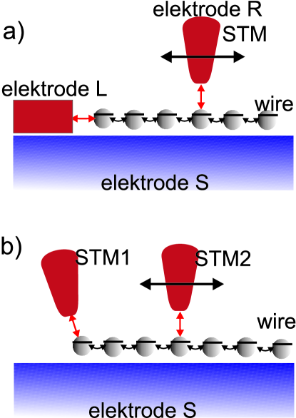
Mono-atomic wires of metal atoms fabricated on a surface are the ultimately small conductors and may be used in nanoelectronics to connect nanodevices such as quantum gates, qubits, or nanotransistors. Thus their electronic properties are of crucial interest. One-dimensional mono-atomic wires can be fabricated using mechanically controlled break junctions 5 ; 6 . Such wires are freely suspended and, thus, do not interact with any substrate. For the same reason, they are somewhat unstable, and it consequently represents a challenge to form long wires. Similar but more stable structures can be fabricated on vicinal surfaces and investigated with scanning tunneling microscopes (STM) 1 ; 2 ; 3 , see Fig. 1. Well ordered and even longer examples are double stranded gold wires grown on silicon vicinal surfaces such as Si(335) and Si(557) 2 ; 3 ; 4 . The geometry and the electronic structure of these setups are sufficiently stable such that measurements can be repeated many times. Notice that STM experiments mainly focus on the electron transport from the STM tip to the surface (perpendicular transport) and, thus, are not concerned with the transport from one end of the wire to the other end. The latter type of STM experiments would require some modifications of the setup as is discussed in Refs. 28 ; Tegen ; Tanik ; Wang0 .
The conductance of ideal or disturbed wires has been investigated both experimentally and theoretically. For example, it has been predicted that the conductance of an atom chain depends on whether the number of atoms is even or odd 7 ; 8 ; 9 ; 10 ; 11 . These even-odd oscillations have been confirmed experimentally 5 . Conductance oscillations with larger periods may occur as well 12 ; 13 ; 14 ; 15 . They stem from a Fabry-Perot like resonance of electrons with Fermi wavelength in the chain, which eventually changes the chain filling factor 12 ; 14 ; 15 . Moreover, the formation of charge waves inside a wire was observed for both, non-magnetic 16 and magnetic wires 17 . The fact that the resonance condition depends on the presence of further atoms beyond the contact also leaves its fingerprints in the conductance, where interference effects can be observed 18 ; 19 ; 20 ; 21 ; 22 ; 23 .
In this paper we consider setups in which one lead is realized by a movable STM tip by which an atom of choice can be contacted; see Fig. 1. We describe the atom chain by a tight-binding Hamiltonian and obtain the conductance within a Green’s function approach 11 ; 14 ; 24 ; 25 ; 26 ; 27 ; HRY ; KohlerPR . It will turn out that the conductance oscillations are influenced by small leakage currents from the wire to the substrate. Our substrate model, the spatial separation of the wire atoms is taken into account by considering local tunnel couplings. A relevant parameter of this model is the Fermi wavelength of the substrate electrons, which allows one to interpolate between two limits: In the one limit, each wire atom couples individually to a substrate with localized electrons, while for the other limit model, the substrate represents a reservoir of delocalized electrons. These two setups may be interpreted as an insulating and a conducting substrate, respectively, or the coupling to a molecule with according localization properties Petrov .
The paper is organized as follows. In Sec. 2 we present our model and a scattering formalism. Moreover, we derive an analytical expression for the retarded Green’s function of a wire coupled to a surface. With these expressions at hand, we investigate in Sec. 3 both conductance oscillations and charge oscillations. The main conclusions are drawn in Sec. 4.
2 Theoretical model and formalism
We consider the setups sketched in Fig. 1 which both consist of a quantum wire connected to two metallic electrodes. The wire may exchange electrons also with the surface which, thus, represents a further, weakly connected electrode. One of these electrodes may be fabricated by epitaxy or grown on the surface and is fixed Wang0 . The other electrode is movable and contacts an atom of choice. Alternatively, both electrodes may be realized by an STM tip as is sketched in Fig. 1(b).
The model Hamiltonian for a wire with atom sites can be written in the form , where
| (1) |
describes the electrons in the wire and in the leads. Electron transitions between the leads and the wire are established by the tunnel Hamiltonian
| (2) |
Here, and label the atom connected to the left and to the right lead, respectively. It is worth mentioning that if the left STM electrode couples to the first wire site, and the right electrode to the last site, , the system corresponds to the break junction geometry of Refs. 5 ; 9 ; 10 ; 11 ; 14 . The operators and create and annihilate, respectively, an electron at site , while and are the according leads operators. The tunnel matrix elements enter the expressions for the current only via the spectral densities , , which we model within a wide-band approximation as energy independent. With the above Hamiltonian we assume that electron-electron interactions do not lead to correlation effects and can be captured by an effective shift of the onsite energies. Then both spin directions are independent of each other, such that the spin need not be considered explicitly. For Au or Pb chains on vicinal silicon surfaces, these conditions are met reasonably well. Generally, this should hold for non-magnetic wire atoms 31 . It has also been shown that electron-electron correlations do not change the period of conductance oscillations 15 ; 29 ; 30 .
In order to describe electron leakage from the wire to the surface, we consider the surface as a further, weakly coupled electrode. Thus, we introduce the wire-surface tunneling Hamiltonian
| (3) |
where is the tunnel matrix element for atom 32 ; 33 . The phase factor reflects the position of atom and has the consequence that the leakage depends on the spatial separation of the atoms. Assuming equal distances between neighboring atoms, while mainly substrate electrons with Fermi wavelength play a role, we obtain . As for the leads, the influence of the substrate can be subsumed in a spectral density. It will turn out that the relevant quantity reads
| (4) |
with the effective leakage strength . A formally similar coupling and spectral density has been used to describe decoherence of spatially separated qubits coupled to a bosonic environment Palma ; DollEPL ; DollPRB . While the fermionic case can still be treated within scattering theory, the bosonic model gives rise to memory effects which may be considered within a non-Markovian master equation approach Kleinekathofer ; Welack ; Weiss
Two limiting cases are worth being discussed: (i) If , the spectral density is rather small unless . This means that we can employ the approximation . This describes a substrate with a very short mean free path such as a semi-conductor or an insulator. Then an electron that tunnels from a particular atom to the substrate can re-enter only at the same site. Obviously, this scheme corresponds to a model in which each wire atom is coupled to an individual additional electrode. (ii) In the opposite limit, , we obtain . Physically this means that the wire electrons tunnel to a delocalized substrate orbital, as is the case for metallic surfaces.
In order to obtain the linear conductance between the electrodes and and the local density of states at site , , one needs to compute the Green’s function for the total Hamiltonian. The linear conductance at zero temperature is given by the Landauer formula 24 ; 25 ; 26 ; 27 ; KohlerPR
| (5) |
where is the electron transmission at the Fermi energy which we choose to be . Using the equation of motion for the retarded Green’s function , one finds the elements from the relation , where the matrix is given by
| (6) |
Below, when presenting specific results, we will always assume that both leads couple equally strong to the wire, yielding , and that all onsite energies and intra-wire tunnel matrix elements are position independent, and . These assumptions are quite reasonable for a wire consisting of one atom species in an equidistant arrangement on the surface.
In the absence of wire-surface tunneling, i.e. for , the matrix becomes tri-diagonal and its inverse, the Green’s function, can be computed analytically. After some algebra we find
| (7) |
where
| (8) |
while denotes the tri-diagonal matrix for , i.e. for the isolated wire. The determinant of this matrix can be evaluated to read , where is the th Chebyshev polynomial of the second kind and plays the role of a Bloch phase 16 . Note that and .
For a wire-surface coupling in the limit (i), the additional self-energy is proportional to the unit matrix, , such that can still be computed analytically. Then we obtain again the Green’s function (7), but with replaced by .
The local density of states at wire site is determined by the retarded Green’s function owing to the relation , where denotes the algebraic complement of the matrix , the so-called cofactor. The charge localized at site can be obtained by integrating the local density of states up to the Fermi energy,
| (9) |
Note, that due to wire-surface coupling, analytical formulas for the local density of states or charge density cannot be simplified further. Thus Eq. (7) is the most general analytical expressions for the retarded Green functions for arbitrary wire length.
3 Conductance oscillations
The conductance of a quantum wire is governed by the electron wave functions at the Fermi surface. In particular for short wires, it may even be such that a single orbital in the relevant energy range dominates. Its overlap with the electrodes may change significantly with the length of the wire and, thus, the conductance changes as well. Typically this change appears as periodic oscillation 7 ; 8 ; 9 ; 10 ; 11 ; 12 ; 13 ; 14 ; 15 . For a break junction geometry, i.e., when the left electrode is connected to the first atom (), and the right electrode to the last atom (), the period of the oscillation can be determined analytically: Writing the transmission in terms of the Green’s function (7), one imposes that this transmission for a wire of length must be the same as for a wire of length . This results in the condition , where 14 . The same relation holds for a wire coupled to a surface.
3.1 Quantum wire isolated from the substrate
Before addressing the influence of a substrate, we study the conductance oscillations of a wire that couples only to the electrodes, but not to the substrate. In particular, we focus on the influence of the wire atoms beyond the STM tips. The presence of these atoms modifies the wave functions of the wire electrons and, consequently, it may affect the overlap between the relevant wire states and the electrodes. In all our numerical studies presented below, we use the Fermi energy as reference point and assume a fixed left electrode i.e. . All energies are measured in units of the wire-electrode coupling , such that formally , while the conductance is plotted in units of the conductance quantum , such that it becomes identical to the dimensionless transmission .
Figure 2 depicts the conductance of wires with various lengths as a function of the tip position ; cf. Fig. 1(a). The onsite energies are position independent, , and chosen such that they satisfy the oscillation condition for period (panels a, b, and c, respectively). A most prominent feature is that the amplitude of the emerging oscillations depends strongly on the total wire length , or put differently, on the number of atoms beyond the right electrode. A closer look at the results for periodicity (panel a) reveals that the amplitude changes with each additional wire atom from a large to a small value and back. For odd , the conductance oscillates with a very large amplitude, whereas for an even number of atoms, these oscillations are very small. Note, that the conductance obtained for any even is hardly distinguishable form the one for . The same holds for any odd and .

For the periods and , we find large oscillation amplitudes for the wire lengths and , respectively. For other lengths, the conductance still oscillates, but its value never exceeds 10% of the conductance quantum. The bottom line of these numerical investigations is that we observe strong oscillations with period provided that the wire has length , where is any natural number 14 . Thus for periods as considered in Fig. 2, maximal amplitudes of the conductance oscillations are observed for
| (10) |
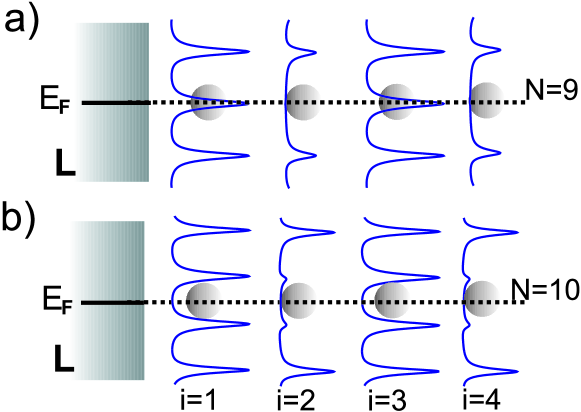
Some insight about the physical origin of the conductance oscillations is provided by considering the local density of states . For a case with even-odd oscillations (), this is shown in Fig. 3 for the wire sites . The magnitude of the conductance can be understood from the fact that for (panel a), the density of states possesses a peak at the Fermi energy. Thus, electrons from the Fermi surface of the left electrode can tunnel to the wire resonantly, which facilitates transport. For length (panel b), by contrast, the density of states at the first site vanishes, such that transport is practically blocked. The density of states at the further sites changes with period . Applying the same arguments to the right STM tip explains that the conductance must oscillate with the same period. In the second case (even ), however, the value of the conductance is small due to the small local density of states at the Fermi energy on the left STM tip . This directly translates to a small oscillation amplitude of the conductance. In the same way one can explain the conductance oscillations with other periods. In general, the conductance is maximal when both STM electrodes are connected to sites that possess a large local density of states at the Fermi level.
A possible application of our results is the experimental estimate of the onsite energy which strongly influences the oscillation periods. However, since also the wire length and the tip position have significant impact on the conductance, it would be necessary to perform several measurement with wires that differ only in length but are identical otherwise.
3.2 Influence of the substrate
The influence of the wire-substrate tunneling can be appreciated in Fig. 4 where we compare the conductance oscillations for two values of with those obtained in the absence of the substrate, i.e. for . Let us first consider the limiting cases in which the substrate electrons are perfectly delocalized () or perfectly localized (). We find two significant features: The oscillation period is practically not influenced by the leakage, while the oscillation amplitude decreases with increasing coupling strength.

Let us now turn to the more realistic intermediate case of finite and its influence on the conductance oscillations, Fig. 5. Typically this parameter is in the range 33 . The onsite energies are chosen such that the oscillation period is or . The results interpolate those for the limiting cases discussed in the previous paragraph. Thus, we can conclude that the value of leaves the oscillation decay qualitatively unchanged, despite the fact that the quantitative difference may be significant.

In Fig. 6, we compare the conductance decay for perfectly localized substrate electrons () and perfectly delocalized electrons () with the one for the intermediate value . One notices that the decay is weaker the more localized the substrate electrons are. It is even such that for , the conductance does not decay entirely, but converges to a finite value. This reminds one to the incomplete decay of entanglement and coherence between delocalized qubits coupled to substrate phonons DollEPL ; DollPRB . A qualitative explanation for the observed dependence on is that an electron that is lost to a delocalized substrate orbital may tunnel back to its former state at any site. In the case of a substrate with localized electrons, by contrast, the lost electron may tunnel back only to the very same wire site. The rates at which these processes occur should differ roughly by a factor , i.e., by the number of wire atoms. This crude estimate agrees roughly with our numerical results provided that and are of the same order.

3.3 Charge oscillations
We already mentioned that the conductance oscillations relate to oscillations of the charge density, which can be observed with STM techniques 34 . Similar charge waves have been predicted for a wire with break junction geometry 16 ; 17 . Thus, one may suspect that the leakage affects the charge oscillations as well. Figure 7 depicts the localized onsite charge as a function of the wire atom position for different surfaces and the oscillation periods (panel a) and (panel b). Interestingly, with increasing leakage, the charge oscillations fade away stronger than the conductance oscillations. Also here, the influence of the leakage is more pronounced the more localized the substrate electrons are. A further common feature is that tunneling to the substrate affects only the oscillation amplitude, while the period remains the same.

4 Conclusions
Using a scattering approach, we have studied conductance and charge oscillations of a quantum wire in contact with a movable electrode. As a particular feature, we considered electron leakage from the wire to various types of substrates. Our model for the latter allows for both strongly localized, weakly localized, and perfectly localized substrate electrons.
As a main feature, we have found that both the conductance oscillations and the localized onsite charge are fading away due to the influence of the substrate. Interestingly, this influence is weaker the more localized the substrate electrons are. For our model, the localization parameter , i.e., Fermi wavelength times the distance of the wire atoms leads to a monotonic transition between the limiting cases of perfect localization and delocalization. In all cases, the oscillation amplitude is smaller than in the absence of the substrate. Thus, leakage represents an obstacle for the experimental observation of conductance oscillations. Nevertheless, a piece of good news is that leakage does not influence the oscillation period. This is rather encouraging, because it implies that conductance oscillations can be observed with wires that are grown on surfaces, despite their unavoidable contact to the wire. We thus are confident that our results will stimulate STM experiments with wires grown on vicinal surfaces.
Acknowledgements.
This work has been supported by Grant No. N N202 1468 33 of the Polish Ministry of Science and Higher Education and by the Alexander von Humboldt Foundation (TK). SK and PH acknowledge support by the DFG via SPP 1243, the excellence cluster “Nanosystems Initiative Munich” (NIM), and the German-Israeli Foundation (GIF, grant no. I 865-43.5/2005 ).References
- (1) R.H.M. Smit, C. Untiedt, G. Rubio-Bollinger, R.C. Segers, J.M. van Ruitenbeek, Phys. Rev. Lett. 91, 076805 (2003).
- (2) N. Agrait, A. Levy Yeyati, J.M. van Ruitenbeek, Phys. Rep. 377, 81 (2003).
- (3) A. Yazdani, D.M. Eigler, N.D. Lang, Science 272, 1921 (1996)
- (4) M. Krawiec, T. Kwapiński, M. Jałochowski, Phys. Stat. Sol. (b) 242, 332 (2005).
- (5) M. Krawiec, T. Kwapiński, M. Jałochowski, Phys. Rev. B 73, 075415 (2006).
- (6) M. Jałochowski, M. Stróźak, R. Zdyb, Surf. Sci. 375, 203 (1997).
- (7) I. Shiraki, F. Tanabe, Rei Hobara, T. Nagao, S. Hasegawa, Surf. Sci. 493, 633 (2001).
- (8) C. Tegenkamp, Z. Kallassy, H. Pfnür, H.-L. Günter, V. Zielasek, M. Henzler, Phys. Rev. Lett. 95, 176804 (2005).
- (9) T. Kanagawa, R. Hobara, I. Matsuda, T. Tanikawa, A. Natori, S. Hasegawa, Phys. Rev. Lett. 91, 036805 (2003).
- (10) K. Wang, X. Zhang, M.M.T. Loy, X. Xiao, Surf. Sci. 602, 1217 (2008).
- (11) H.-S. Sim, H.-W. Lee, K.J. Chang, Phys. Rev. Lett. 87, 096803 (2001).
- (12) T.-S. Kim, S. Hershfield, Phys. Rev. B 65, 214526 (2002).
- (13) N.D. Lang, Phys. Rev. Lett. 79, 1357 (1997).
- (14) N.D. Lang, Ph. Avouris, Phys. Rev. Lett. 81, 3515 (1998).
- (15) Z.Y. Zeng, F. Claro, Phys. Rev. B 65, 193405 (2002).
- (16) P.L. Pernas, F. Flores, E.V. Anda, J. Phys.: Condens. Matter 4, 5309 (1992).
- (17) K.S. Thygesen, K.W. Jacobsen, Phys. Rev. Lett. 91, 146801 (2003).
- (18) T. Kwapiński, J. Phys.: Condens. Matter 17, 5849 (2005).
- (19) R.A. Molina, D.Weinmann, J.-L. Pichard, Europhys. Lett. 67, 96 (2004).
- (20) T. Kwapiński, J. Phys.: Condens. Matter 18, 7313 (2006).
- (21) M. Mierzejewski, M.M. Maska, Phys. Rev. B. 73, 205103 (2006).
- (22) Sz. Csonka, A. Halbritter, G. Mihály, E. Jurdik, O.I. Shklyarevskii, S. Speller, H. van Kempen, Phys. Rev. Lett. 90, 116803 (2003).
- (23) Sz. Csonka, A. Halbritter, G. Mihály, O.I. Shklyarevskii, S. Speller, H. van Kempen, Phys. Rev. Lett. 93, 016802 (2004).
- (24) R.H.M. Smit, Y. Noat, C. Untiedt, N.D. Lang, M.C. van Hemert, J.M. van Ruitenbeek, Nature 419, 906 (2002).
- (25) K.S. Thygesen, M. Bollinger, K.W. Jacobsen, Phys. Rev. B 67, 115404 (2003).
- (26) M.E. Torio, K. Hallberg, A.H. Ceccatto, C.R. Proetto, Phys. Rev. B 65, 085302 (2002).
- (27) T. Kwapiński, J. Phys.: Condens. Matter 19, 176218 (2007).
- (28) V. Mujica, M. Kemp, M.A. Ratner, J. Chem. Phys. 101, 6849 (1994).
- (29) R. Landauer, Philos. Mag. 21, 863 (1970).
- (30) C. Caroli, R. Combescot, D. Lederer, P. Nizieres, D. Saint-James, J. Phys. C 4, 2598 (1971).
- (31) S. Datta “Electonic transport in mesoscopic systems” (Cambridge Univ. Press, 1995).
- (32) P. Hänggi, M. Ratner, and S. Yaliraki, Chem. Phys. 281, 111 (2002).
- (33) S. Kohler, J. Lehmann and P. Hänggi, Phys. Rep. 406, 379 (2005).
- (34) E. G. Petrov, Low Temp. Phys. 31, 338 (2005).
- (35) P.A. Orellana, F. Dominguez-Adame, I. Gómez, M.L. Ladrón de Guevara, Phys. Rev. B 67, 085321 (2003).
- (36) M. Krawiec, T. Kwapiński, Surf. Sci. 600, 1697 (2006).
- (37) A. Oguri, Phys. Rev. B 59, 12240 (1999).
- (38) D.M. Newns, N. Read, Adv. Phys. 36, 799 (1987).
- (39) M. Krawiec, M. Jałochowski, Phys. Stat. Sol. (b) 244, 2464 (2007).
- (40) G.M. Palma, K.-A. Suominen, A.K. Ekert, Proc. R. Soc. London, Ser. A 452, 567 (1996)
- (41) R. Doll, M. Wubs, P. Hänggi, S. Kohler, Europhys. Lett. 76, 547 (2006)
- (42) R. Doll, M. Wubs, P. Hänggi, S. Kohler, Phys. Rev. B 76, 045317 (2007)
- (43) U. Kleinekathofer, J. Chem. Phys. 121, 2505 (2004).
- (44) S. Welack, M. Schreiber, U. Kleinekathofer, J. Chem. Phys. 124, 044712 (2006).
- (45) S. Weiss, J. Eckel, M. Thorwart, R. Egger, Phys. Rev. B 77, 249901 (2008).
- (46) M.F. Crommie, C.P. Lutz, D.M. Eigler, Science 262, 218 (1993).