Quantum confinement effects in Si/Ge heterostructures with spatially ordered arrays of self-assembled quantum dots
Abstract
Magnetotunneling spectroscopy was employed to probe the confinement in vertical Si/Ge double-barrier resonant tunneling diodes with regularly distributed Ge quantum dots. Their current-voltage characteristics reveal a step-like behavior in the vicinity of zero bias, indicating resonant tunneling of heavy-holes via three-dimensionally confined unoccupied hole states in Ge quantum dots. Assuming parabolic confinement we extract the strength of the confinement potential of quantum dots.
pacs:
78.20.Ls, 73.21.La, 75.70.CnThe unique high frequency characteristics of resonant tunneling diodes made them suitable for use in a variety of electronics applications Brown01Paper89 ; Mazumder03Paper98 ; McMeekin01Paper96 . The progress in semiconductor technology turned materials like Si, Ge and Si1-xGex to promising ones for the development of the semiconductor devices, based on the phenomena of quantum tunneling of charge carriers through potential barriers. There are nevertheless some natural properties of these materials restricting their applicability, for instance for optical applications due to the indirect band gap of these materials. It was shown Brunner02Review02 that Si/Ge heteroepitaxy on prepatterned substrates leads to the formation of regimented arrays of self-assembled quantum dots (QDs) with predefined ordering and geometry being an effective way to improve electronic and optical properties of Si/Ge heterostructures. Here we report on the study of confinement properties of two-terminal devices, based on the quantum tunneling through Ge QDs of definite spatial distribution.
The double-barrier resonant tunneling diodes (DBRTD), investigated in this work, were processed of a Si/Ge heterostructure, grown by molecular beam epitaxy on a prepatterned p−Si (100) substrate with a resistivity of 0.02−0.08 . To obtain a substrate having a two-dimensional (2D) pit pattern with a periodicity of 280 280 nm2, extreme ultraviolet interference lithography (EUV-IL) at a wavelength of 13.5 nm was used Auzelyte01Paper09 ; Dais02Paper08 . The EUV-IL was performed at the Swiss Light Source at the Paul Scherrer Institut and the light exposing dose was chosen to be as high as 250 mW/cm2. The exposed pit pattern was transferred into the Si substrate by reactive ion etching down to a depth of 10 nm Dais02Paper08 .
The first layer grown on the substrate is a 250 Å thick boron doped p+–Si buffer layer (p 5 1018 cm-3). It is followed by 200 Å of strained p+-doped Si1-xGex with graded Ge content () ranging from 0.05 to 0.30 and the same doping concentration as in the Si buffer layer. After this first Si1-xGex film an undoped Si barrier with a thickness of 50 Å is grown. Next, six monolayers (6 ML) of strained Ge are deposited. By growing of a Ge film with a thickness of 6 ML, we exceed the critical thickness for the realization of 2D planar deposition of Ge on Si, which is about 3 monolayers. This exceedance leads to the formation of self-assembled Ge QDs in our heterostructure. The second barrier of identical parameters as the first one clads the germanium film. This barrier is in turn overgrown by the second graded Si1-xGex layer, similar to the first one. At last a 7000 Å thick p+-doped Si cap layer follows. All the layers except that of Ge were grown at a substrate temperature 300 \celsius. During the growth process of Ge the temperature was ramped from 300 up to 470 \celsius to improve the homogeneity of the dot nucleation and their spatial distribution.
Despite the low deposition temperature strain- and temperature-induced intermixing of the Ge islands with Si of the lower barrier takes place Patriarche01Paper00 , leading to the formation of Si1-xGex alloy with a nonhomogeneous distribution of Ge content Kirfel01Paper04 . The photoluminescence and X–ray diffractometry measurement data, obtained on similarly grown heterostructures, let us assume an average Ge content in our QDs to be about 50 %.
An uncapped test sample with 6 ML of Ge (exposed to EUV light of the same dose of 250 mW/cm2) was grown to investigate its topography. The inset of Fig. 1 shows an atomic force microscopy (AFM) image of its surface. The interplay of strain and surface tension of the deposited Ge layer results in the formation of regimented arrays of up to four (105)-faceted 3D Ge hut clusters (further referred to simply as QDs) per prepatterned pit.
A strained Si/Ge heterostructure with Ge QDs forms a type-II heterojunction. Its band alignment creates a potential well only for the holes within the Ge dots Yakimov02Paper01 . As our heterostructure is strained, the heavy-hole (HH) band in the Si1-xGex emitter becomes decoupled from the light-hole (LH) and split-off bands Pikus . We assume that due to the band splitting only HH states are occupied in the emitter at 100 mK. Thus, we consider only HH take part in the charge transport.
The vertical DBRTDs were processed using electron-beam lithography, wet-etching and polyimide isolation technique to support the top contacting pads Reed02Paper88 ; Tewordt01Paper91 . The diameter of the diodes varies between 1 and 2 m. Transport measurements were made in a dilution refrigerator in the temperature range from 100 mK to 1 K. A homogeneous magnetic field was applied perpendicular (angle 90∘ in our notation) and parallel (0∘) to the heterointerface. The current-voltage (IV) characteristics were measured in a 2-point measurement technique. The forward bias refers to the positively biased bottom electrode (substrate) of the diode.
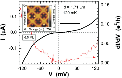
Figure 1 shows the IV-characteristic (along with its derivative ) of a vertical DBRTD with the cross-section diameter of d = 1.71 m. The measurement was carried out at and 120 mK. We do not observe, on the characteristics of our diodes with QDs, any strongly expressed resonant current peak which is typical for a DBRTD with a quantum well. The reason for the absence of a peak could lay in the complicated heterostructure interface profile due to the substrate prepatterning along with the possible dopant diffusion from the highly doped Si1-xGex regions into the barriers due to the absence of an undoped spacer between them, which could destroy the resonant tunneling characteristics. We emphasize that our samples do not contain a quantum well but quantum dots.
The clearly nonlinear IV-characteristic reveals a lot of features in its derivative. The slight asymmetry of the characteristic in forward and reverse bias is due to the difference in the substrate and top electrode doping Zaslavsky01Paper92 . In the bias range 60 mV a set of small current steps on the IV-characteristic along with the corresponding peaks in the are resolved for both polarities of applied voltage. At higher bias this peak structure washes out.
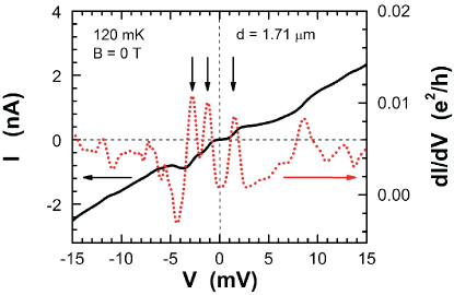
From the temperature dependent broadening of the correspondent current step edge, we have determined the energy–to–bias conversion factor Su02Paper98 . It turned out to be equal to 0.49 meV/mV for the three well pronounced peaks in the vicinity of zero bias, which are marked by vertical arrows in Fig. 2. There are other peaks that appear at higher voltages ranging from 15 to 35 mV. For these peaks we find 0.15 meV/mV, which is quite different compared to for the peaks mentioned above. Therefore, the observed peaks can be divided into two groups according to the correspondent values of . We attribute the peaks in the vicinity of zero bias to resonant tunneling of HH from the emitter electrode into the three-dimensionally confined discrete HH states within the QDs. Taking into account an average distance of 117 nm between the QDs within the arrays, we conclude that the above mentioned tunneling occurs through the individual quantum dots and not over the array as a whole. The group of peaks at higher voltages is assigned to tunneling events through impurities located outside the Ge layer, namely, in the Si barriers.
Magnetotunneling spectroscopy has proven to be a very powerful and informative method for the investigation of electron Goldman01Paper87 ; Leadbeater03Paper89 and hole Eaves03Paper92 ; LiuJ03Paper00 dynamics in DBRTDs. We have applied magnetic fields up to 12 T parallel () and perpendicular () to the heterointerface to resolve the strength of the confinement potential and to investigate its effect on the transport properties of our DBRTD.
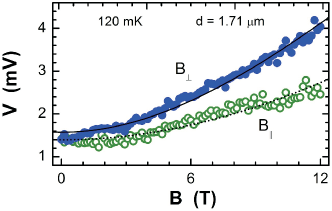
Under the influence of increasing magnetic fields of both and orientations, we observed a noticeable shift of all peaks from their initial voltage position at 0. For the peaks, appearing in the vicinity of zero bias, the shift additionally turned out to be field orientation dependent. We concentrate our discussion on these three peaks from Fig. 2. Figure 3 shows the field dependent evolution of the peak being observed at the bias mV for 0. It shows a clear difference in the peak shift under (open circles) and (filled circles). From these observed shifts we can gain information about the hole confinement in our QDs.
For the data analysis, we have made the following assumptions and simplifications. We neglect spin effects and valence band intermixing. We treat the HH in the QDs of our sample as parabolically confined in all three spatial directions and suppose that all three peaks in the vicinity of zero voltage correspond to tunneling over the lowest HH states. The expression to describe the ground state energy of a single particle confined by a parabolic potential is given by
| (1) |
where accounts for the voltage position of the correspondent peak at , is the effective mass, is a radial distance, is the confinement energy and is the cyclotron frequency.
As was mentioned above, we suppose the Ge fraction of Si1-xGex alloy forming the QDs to be of the order of 0.5. We neglect the effect of the strain on the HH effective mass and for simplicity treat it also as isotropic. Thus is estimated according to Ref. Paul01Review04 from the Luttinger parameters , determined from Ref. Schaeffler01Paper97 . Here is the free electron mass. Using (1) we have performed fits on the experimental voltage position data sets for all peaks discussed in this work. The obtained fitting curves match our experimental data quite well. In Fig. 3 two best-fitting curves (solid and dotted) for the peak appearing at mV ( 0) are shown. In Ref. Rego01Paper97 the hole states in p-type quantum disks in magnetic field were studied theoretically. A similar increase of the lowest-lying HH ground state energy under the influence of the rising magnetic field as observed in our experiment is reported there.
The important result of the fitting procedure consists in revealing a value for the QD confinement potential. For the two fit curves in Fig. 3 we obtained 2.64 meV under and 5.9 meV under . For the other two peaks of this group similar values were obtained. The observed difference in for two mutually perpendicular magnetic field directions is consistent with the expectation, that due to the geometrical factors the lateral confinement (revealed under the ) should be weaker compared to the confinement in the QDs growth direction.
As was mentioned the peaks observed far from zero voltage originate from HH resonant tunneling via impurities located within Si barriers. Contrary to the peaks discussed above these peaks do not show field orientational dependence of their voltage position. This indicates the symmetry of the confinement potential. The fitting based on the assumption of the isotropic revealed for both magnetic field orientations almost equal values 21 meV. This result supports the idea about tunneling over impurities having much smaller size than QDs and thus apparently stronger confining properties. Calculations taking into account the possible anisotropy of (Ref. Schuberth01Paper91 ) reveal for these peaks what would contradict our experimental observations.
To conclude, we have investigated the electric transport properties of DBRTDs with regularly ordered self-assembled Ge quantum dots. Steplike structures in the IV-characteristic and corresponding sharp peaklike structures are revealed. We attribute the peaks in the vicinity of zero voltage to resonant tunneling of HH through confined discrete HH states within QDs. The peaks at higher voltage originate from the resonant tunneling via impurities located in Si barriers. With the help of magnetotunneling spectroscopy, assuming a parabolic confinement and an isotropy of we have obtained values for the strength of the confinement potential for impurities and for quantum dots.
References
- (1) E. R. Brown , T. C. L. G. Sollner , C. D. Parker , W. D. Goodhue and C. L. Chen , Appl. Phys. Lett. 55, 1777 (1989).
- (2) P. Mazumder, S. Kulkarni, M. Bhattcharya, J. P. Sun and G. I. Haddad , Proc. IEEE 86, 664 (1998).
- (3) S. G. McMeekin, M. R. S. Taylor, C. N. Ironside, IEE Proc.: Optoelectron. 143, 12 (1996).
- (4) K. Brunner, Rep. Prog. Phys. 65, 27 (2002).
- (5) V. Auzelyte, C. Dais, P. Farquet, D. Grützmacher, L. J. Heyderman, L. Feng, S. Olliges, C. Padeste, P. K. Sahoo, T. Thomson, A. Turchanin, C. David, H. H. Solak, J. Micro/Nanolith. MEMS MOEMS 8, 021204 (2009).
- (6) C. Dais, H. H. Solak, E. Müller, and D. Grützmacher, Appl. Phys. Lett. 92, 143102 (2008).
- (7) G. Patriarche, I. Sagnes, P. Boucard, V. Le Thanh, D. Bouchier, C. Hernandez, Y. Campidelli, D. Bensahel, Appl. Phys. Lett. 77, 370 (2000).
- (8) O. Kirfel, E. Müller, D. Grützmacher, K. Kern, A. Hesse, J. Stangl, V. Holý, G. Bauer, Appl. Surf. Sci. 224, 139 (2004).
- (9) A. V. Dvurechenskiĭ, A. I. Yakimov , Physics–Uspekhi 44(12), 1304 (2001).
- (10) G. L. Bir and G. E. Pikus, Symmetry and Strain-Induced Effects in Semiconductors (Wiley, New York, 1974)
- (11) M. A. Reed, J. N. Randall, R. J. Aggarwal, R. J. Matyi, T. M. Moore, and A. E. Wetsel, Phys. Rev. Lett. 60, 535 (1988).
- (12) M. Tewordt, V. J. Law, M. J. Kelly, R. Newbury, M. Pepper, D. C. Peacock, J. E. F. Frost, D. A. Ritchie and G. A. C. Jones, J. Phys.: Condens. Matter 2, 8969 (1991).
- (13) A. Zaslavsky, D. A. Grützmacher, Y. H. Lee, W. Ziegler, and T. O. Sedgwick, Appl. Phys. Lett. 61, 2872 (1992).
- (14) B. Su, V. J. Goldman, and J. E. Cunningham, Phys. Rev. B 46, 7644 (1992).
- (15) V. J. Goldman, D. C. Tsui, and J. E. Cunningham, Phys. Rev. B 35, 9387 (1987).
- (16) M. L. Leadbeater, E. S. Alves, L. Eaves, M. Henini, O. H. Hughes, A. Celeste, J. C. Portal, G. Hill and M. A. Pate, Phys. Rev. B 39, 3438 (1989).
- (17) L. Eaves, R. K. Hayden, M. L. Leadbeater, D. K. Maude, E. C. Valadares, M. Henini, F. W. Sheard, O. H. Hughes, J. C. Portal and L. Cury, Surface Science 263, 199 (1992)
- (18) J. Liu, A. Zaslavsky, C. D. Akyüz, B. R. Perkins, and L. B. Freund, Phys. Rev. B 62, R7731 (2000).
- (19) D. J. Paul, Semicond. Sci. Technol. 19, R75 (2004).
- (20) F. Schäffler, Semicond. Sci. Technol. 12, 1515 (1997).
- (21) L. G. C. Rego, P. Hawrylak, J. A. Brum, and A. Wojs, Phys. Rev. B 55, 15694 (1997)
- (22) G. Schuberth, G. Abstreiter, E. Gornik, F. Schäffler, and J. F. Luy, Phys. Rev. B 43, 2280 (1991).