Surface-driven electronic structure in LaFeAsO studied by angle resolved photoemission spectroscopy
Abstract
We measured the electronic structure of an iron arsenic parent compound LaFeAsO using angle resolved photoemission spectroscopy (ARPES). By comparing with a full-potential Linear Augmented Plane Wave calculation we show that the extra large hole pocket measured via ARPES comes from electronic structure at the sample surface. Based on this we discuss the strong polarization dependence of the band structure and a temperature-dependent hole-like band around the point. The two phenomena give additional evidences for the existence of the surface-driven electronic structure.
pacs:
74.25.Jb, 74.70.Dd, 79.60.BmI Introduction
The discovery of superconductivity in the iron arsenic FeAsO1-xFy family Original (the “1111” family, being the rare earth elements) has triggered enormous scientific activity within the last two years. The transition temperature in these materials well exceeds the theoretical maximum predicted by the Bardeen-Cooper-Schrieffer theory. Though several other families of iron pnictide superconductors (e.g. the carrier-doped Fe2As2 or the “122” family, being Ba, Sr, Ca, Rh) were discovered after the initial work,Original_122 ; Original_111 ; Original_11 the 1111 family still holds the record for the highest of 55 K.Ren_55K There has been an ongoing debate as to the origin of superconductivity in the iron pnictides as well as their relation to the traditional copper oxide high- superconductors. Recently Yan et al. reported the successful growth of millimeter-sized LaFeAsO single crystals at ambient pressure.Yan_1111 This technical breakthrough brings experimental studies of these fascinating materials to a new height.
Although angle resolved photoemission spectroscopy (ARPES) has proven to be a useful experimental method in the field of the pnictides,Shen_LaOFeP ; Shen_PhysicaC ; Liu_1111FS ; Ding_gap ; Zhou_gap ; Feng_splitting ; Terashima_Cogap ; Hasan_gap one major obstacle has hindered an extensive survey of the 1111 systems. Apparently the Fermi surface (FS) measured by ARPES is inconsistent with the theoretical predictions and other experimental probes of the bulk electronic structure. More specifically, theoretical calculations and quantum oscillation measurements McDonald_dHvA suggest similar sizes of the hole pockets and the electron pockets at the FS, while ARPES shows an extra large circular hole pocket around the zone center , which covers almost 40% of the Brillouin zone intersection size.Liu_1111FS ; Shen_PhysicaC Base on the fact that ARPES can probe only the first layers of the crystal, many authors believe that the extra hole pocket comes from surface-driven electronic structure, i.e. an atomic reorganization and/or lattice relaxation at the sample surface.Shen_PhysicaC ; Mazin_PhysicaC ; Eschrig The answer to this question is a prerequisite for any further ARPES investigation of the 1111 system.
The first propose for this paper is to verify the observation of a surface-driven electronic structure in the 1111 parent compound LaFeAsO. By comparing with an electronic structure calculation for the surface layers, we show that indeed the extra hole pocket comes from a surface FeAs or LaO layer. Despite this, the observation does not exclude the possibility that electronic structure from the bulk crystal is also present in the same ARPES map. Furthermore, it is likely that such a surface-driven hole pocket may store the superconducting information of the bulk crystal via the proximity effect, resulting in e.g. the observation of an -wave-like superconducting gap by Kondo et al.Takeshi_gap Keeping this in mind, we discuss the strong polarization dependence of the band structure and an unusual temperature-dependent hole-like band around the point.
II Experimental
Millimeter-sized single crystals of LaFeAsO were grown out of a NaAs flux using conventional high-temperature solution growth techniques.Yan_1111 As-grown crystals have typical dimensions of with the crystallographic -axis perpendicular to the plane of the plate-like single crystals. The characteristic temperatures for the separated structural and magnetic transitions are K and * K, respectively. The ARPES measurements were performed at beamline 10.0.1 of the Advanced Light Source (ALS), Berkeley, California using a Scienta R4000 electron analyzer, as well as a laboratory-based ARPES system consisting of a Scienta SES2002 electron analyzer, GammaData® UV lamp and custom designed refocusing optics at Ames Laboratory. Vacuum conditions were better than torr. The energy resolution was set at 15 meV for measurements at the ALS, and 9 meV for measurements at Ames Laboratory. All samples were cleaved in situ yielding mirror-like, clean - surfaces. Cleaved surfaces of all samples are stable for at least 24 hours for a given temperature. High symmetry points and are defined to be (, , 0) and (, , 0), respectively,symmetry_points with the and axes along the Fe-As bonds.
III Results and discussion
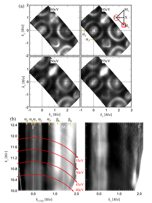
Fig. 1(a) shows the ARPES FS maps of LaFeAsO taken with a linearly polarized synchrotron beam for four different incident photon energies (probing at four different momentaHufner ). More than half of the first Brillouin zone is covered. The data in Fig. 1(a) is consistent with previous ARPES studies on LaFePO, LaFeAsO, CeFeAsO and NdFeAsO0.9F0.1 single crystals.Liu_1111FS ; Shen_PhysicaC ; Zhou_CeFeAsO The most apparent difference between the ARPES data on these 1111 systems and that on the 122 systems is a ultra large Fermi pocket around , which is denoted as throughout the paper. Subsequent band structure analysis [Fig. 3(a)] shows that this pocket is hole-like. This pocket is not expected from theoretical calculationsLiu_1111FS and experimental results for the bulk electronic structure.McDonald_dHvA Recall that the electron escape depth for ARPES experiments are of the order of only a few angstroms (comparable with the lattice constant ), ARPES is essentially a surface probe.Hufner It is thus reasonable to speculate that the existence of the pocket is a result of a surface-driven electronic structure. The dispersion maps in Fig. 1(b) give further evidence for this speculation. It can be easily seen from Fig. 1(b) that the detected electronic structure, including the pocket, is essentially two dimensional along both - and - directions. This observation is in sharp contrast with the three-dimensional electronic structure observed in 122 compounds,Liu_3D ; Brouet while consistent with the two dimensional nature of the sample surface layer.
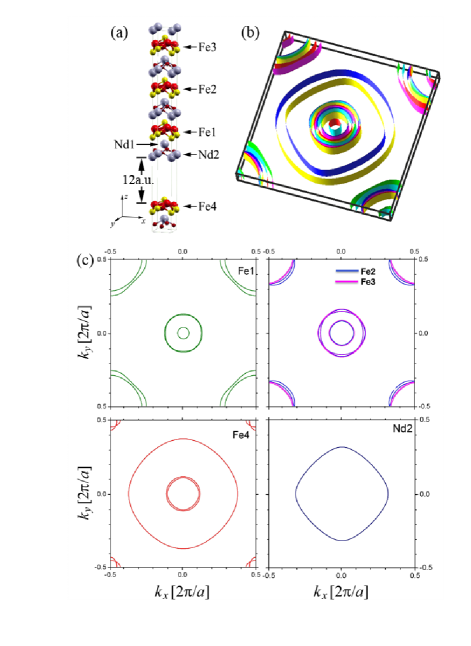
In Fig. 2 we present the results of a model theoretical calculation to verify the existence of the surface-driven electronic structure. It should be noted here that although this calculation is performed for NdFeAsO, the results for LaFeAsO will be essentially the same (see also Ref. Eschrig ), since the 4 electrons of the Nd atoms were treated as core electrons, the valence electrons of the Nd atoms are the same as those of the La atoms. In this calculation we use a full-potential Linear Augmented Plane Wave (FPLAPW) methodLAPW with a local density functional.LDA The structural data was taken from a reported experimental result.Qiu The presence of the crystal surface is imitated by constructing a supercell with four NdO and FeAs layers, and a 12 a.u. vacuum located between the Nd2 and Fe4 layer [Fig. 2(a)]. To obtain the self-consistent charge density, we chose 28 -points in the irreducible Brillouin zone, and set to 7.5, where is the smallest muffin-tin radius and is the plane-wave cutoff. We use the muffin-tin radii of 2.4, 2.1, 2.1 and 1.6 a.u. for Nd, Fe, As and O respectively. In this calculation, the atoms near the surface (Nd1-O-Nd2, As-Fe4-As) were relaxed along the -direction until the forces exerted on the atoms were less than 2.0 mRy/a.u. With this optimized structure, we obtained a self consistency with 0.01 mRy/cell total energy convergence. After that, the three dimensional Fermi surface calculation was performed with 420 -points in the irreducible Brillouin zone [Fig. 2(b)].XcrysDen For the two dimensional electronic structure, we chose (the - plane that crosses the point) and divided the Brillouin zone (, ) into a mesh that resulted in 2601 -points [Figs. 2(c) and 2(d)].
From Figs. 2(b)-(d), one essential statement must be pointed out: The surface layer of NdFeAsO (and LaFeAsO), regardless of its elemental nature (NdO/LaO or FeAs), will generate an extra large hole pocket at the Fermi surface, and this large hole pocket can only be generated at the surface layer of the Nd/LaFeAsO crystal. In contrast, even though it is just the second layer from the surface, the Fe1 layer generates two pockets which are even smaller than the pockets from the same layer. Similar sizes of the and pockets are seen only from the Fe2 and Fe3 layers, which are farther away from the surface and can thus be considered “bulk” states. Assuming the validity of the rigid band shifting scheme, this effect can be explained by the transfer of charge near the surface: electrons are retrieving from the surface layer (Fe4 or Nd2) to the adjacent layer (Fe1), leaving the opposite sign of the electron-hole imbalance for these two layers.
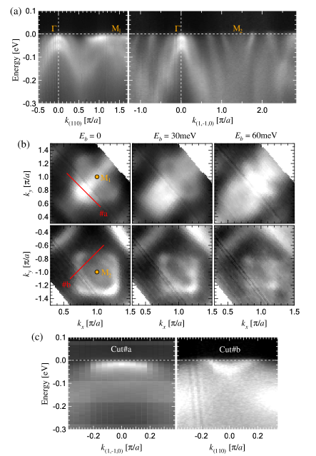
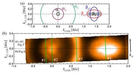
Another interesting observation of Fig. 1 is the strong polarization dependence of the electron pockets. As seen from Fig. 1(a), the two -points and which are away in the -space show fundamentally different electronic structures. Fig. 3 shows their detailed band structure analysis. Clearly the point is surrounded by four petal-like intensity peaks at the chemical potential. The ones along the direction [Cut#a in Fig. 3(c)] are much more pronounced in intensity, and they are indeed hole-like bands, the top of which located at 20meV below the chemical potential. We denote this band as [Fig. 4(a)]. The intensity peaks along the direction are actually part of an elliptical electron pocket. On the other hand, the bands around the point manifest themselves as two crossed elliptical electron pockets [Cut#b in Fig. 3(c)]. We denote them as and [Fig. 4(a)]. We speculate that one of these electron pockets - the one whose long axis is perpendicular to the - direction, - is the same pocket as the one observed around . The only way to explain this unusual behavior is that these -pockets are highly sensitive to the polarization of the incoming beam. In fact such phenomena are observed and discussed in detail in the 122 systems.Hasan_pol ; Feng_pol In Fig. 1 and Fig. 3 in this paper, the electric field vector of the incoming light is polarized along the direction. The entrance slit of the electron analyzer is perpendicular to the mirror plane defined by the incident beam and the sample surface normal. The fact that the and pockets have different parity nature is consistent with tight-binding calculations.Graser
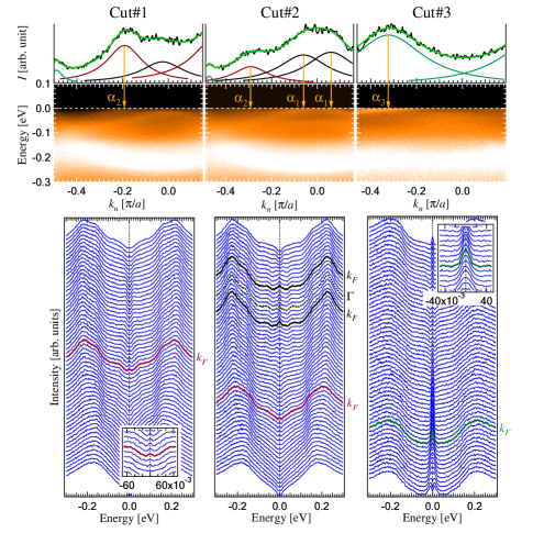
We now move on to a detailed discussion of how these bands/pockets behave at the Fermi level. The high energy resolution data is taken with a partially polarized helium lamp ( eV). We begin this discussion with Fig. 5 where we analyze three - maps marked #1, #2 and #3 in Fig. 4(b). These maps are chosen so that all three hole pockets , and are visible. The main conclusion of this figure is that there is no gap opening at the pockets. In the symmetrized energy distribution curves (EDCs) at each Fermi crossing momenta, we see one single peak instead of two peaks separated by a valley. This is a typical indication of a vanishing gap. Linking this result with the findings by Kondo et al.,Takeshi_gap we obtain an interesting picture for the low lying electronic excitations of this 1111 system. Resulted solely from the surface layer, the pocket shows no gap in the undoped sample, while exhibits an -wave-like gap as large as meV in the fluorine-doped superconducting sample.Takeshi_gap The coherent peak for this gap vanishes right at .Liu_1111FS To date we have no information on whether the surface layer of the 1111 crystal is superconducting itself, so a possible scenario is the proximity effect. The proximity effect offers us the possibility that the superconducting properties of the bulk sample affects the surface. In that case the momentum dependence of the superconducting gap observed for the surface will be similar to that of the bulk crystal. For high- cuprates, it is proposed that the proximity effect may result in “+”-wave superconductivity at the metallic layer that is coated on the superconductor.Kohen ; Sharoni ; Lofwander This scenario is consistent with scanning tunneling spectroscopy (STS) results on polycrystalline 1111 samples where a reduced superconducting gap is observed at the sample surface.Millo ; Pan It is not understood why the gap size shown by ARPES is much bigger than by STS and other methods.
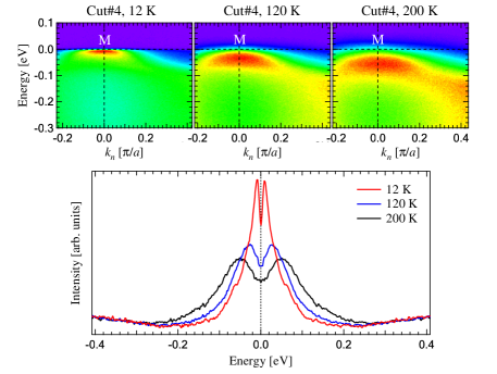
In Fig. 6 we discuss the temperature dependence of the band. Cut#4 is located right through the point where the binding energy is the lowest for this band. One can easily see from Fig. 6 that the peak location of the band gradually shifts to higher binding energies with increasing temperature. At K the maximum intensity is located at meV, whereas at K it shifts to meV. The peak intensity decreases at the same time. Such changes are intrinsic, since multiple measurements are performed in multiple samples, and both increasing and decreasing the temperature during the measurement reveals the same behavior. As a reminder, in the 122 systems the bands locate at the same binding energies until the magnetic transition temperature is reached.Feng_splitting ; Liu_3D ; Zhou_recon ; Shen_recon Here the band location shifts even below the transition temperature (between 12 and 120 K). This is not expected from the bulk properties - transport measurements unambiguously show a magnetic transition at 140 K. It is thus another evidence for the existence of a temperature-dependent surface layer.
IV Conclusions
The main conclusion of this paper is that the surface-driven electronic structure plays an important role in the ARPES data of the iron arsenic 1111 systems. It is a fact that ARPES data on these systems shows more discrepancies rather than agreements with theoretical and experimental bulk properties. ARPES shows a temperature-dependent band, and most significantly an extra large hole pocket around . However, bulk calculations and experiments suggest a Fermi surface reconstruction associating with a well-defined magnetic transition temperature, and similar sizes of and pockets. By comparison with a full-potential Linear Augmented Plane Wave calculation on the surface layers of the crystal, we confirm that at the very least the large pocket is generated solely by the sample surface. The -wave-like superconducting gap that exists in this pocket in the superconducting samples is most likely a result of the superconducting proximity effect.
V Acknowledgments
We thank S.-K. Mo for his grateful instrumental support at ALS. Ames Laboratory was supported by the Department of Energy - Basic Energy Sciences under Contract No. DE-AC02-07CH11358. ALS is operated by the US DOE under Contract No. DE-AC03-76SF00098.
References
- (1) Yoichi Kamihara, Takumi Watanabe, Masahiro Hirano, and Hideo Hosono, J. Am. Chem. Soc. 130, 3296 (2008).
- (2) Marianne Rotter, Marcus Tegel, and Dirk Johrendt, Phys. Rev. Lett. 101, 107006 (2008).
- (3) X. C. Wang, Q. Q. Liu, Y. X. Lv, W. B. Gao, L. X. Yang, R. C. Yu, F. Y. Li, and C. Q. Jin, Solid State Commun. 148, 538 (2008).
- (4) Fong-Chi Hsu, Jiu-Yong Luo, Kuo-Wei Yeh, Ta-Kun Chen, Tzu-Wen Huang, Phillip M. Wu, Yong-Chi Lee, Yi-Lin Huang, Yan-Yi Chu, Der-Chung Yan and Maw-Kuen Wu, Proc. Natl. Acad. Sci. USA 105, 14262 (2008).
- (5) Zhi-An Ren, Wei Lu, Jie Yang, Wei Yi, Xiao-Li Shen, Zheng-Cai Li, Guang-Can Che, Xiao-Li Dong, Li-Ling Sun, Fang Zhou, and Zhong-Xian Zhao, Chin. Phys. Lett. 25, 2215 (2008).
- (6) J.-Q. Yan, S. Nandi, J. L. Zarestky, W. Tian, A. Kreyssig, B. Jensen, A. Kracher, K. W. Dennis, R. J. McQueeney, A. I. Goldman, R. W. McCallum, and T. A. Lograsso, Appl. Phys. Lett. 95, 222504 (2009).
- (7) D. H. Lu, M. Yi, S.-K. Mo, A. S. Erickson, J. Analytis, J.-H. Chu, D. J. Singh, Z. Hussain, T. H. Geballe, I. R. Fisher, and Z.-X. Shen, Nature (London), 455, 81 (2008).
- (8) D. H. Lu, M. Yi, S.-K. Mo, J. G. Analytis, J.-H. Chu, A. S. Erickson, D. J. Singh, Z. Hussain, T. H. Geballe, I. R. Fisher, and Z.-X. Shen, Physica C 469, 452 (2009).
- (9) Chang Liu, Takeshi Kondo, A. D. Palczewski, G. D. Samolyuk, Y. Lee, M. E. Tillman, Ni Ni, E. D. Mun, R. Gordon, A. F. Santander-Syro, S. L. Bud’ko, J. L. McChesney, E. Rotenberg, A. V. Fedorov, T. Valla, O. Copie, M. A. Tanatar, C. Martin, B. N. Harmon, P. C. Canfield, R. Prozorov, J. Schmalian and A. Kaminski, Physica C 469, 491 (2009).
- (10) H. Ding, P. Richard, K. Nakayama, K. Sugawara, T. Arakane, Y. Sekiba, A. Takayama, S. Souma, T. Sato, T. Takahashi, Z. Wang, X. Dai, Z. Fang, G. F. Chen, J. L. Luo, and N. L. Wang, Europhys. Lett. 83, 47001 (2008).
- (11) Lin Zhao, Haiyun Liu, Wentao Zhang, Jianqiao Meng, Xiaowen Jia, Guodong Liu, Xiaoli Dong, G. F. Chen, J. L. Luo, N. L. Wang, Guiling Wang, Yong Zhou, Yong Zhu, Xiaoyang Wang, Zhongxian Zhao, Zuyan Xu, Chuangtian Chen, and X. J. Zhou, Chin. Phys. Lett. 25, 4402 (2008).
- (12) L. X. Yang, Y. Zhang, H. W. Ou, J. F. Zhao, D. W. Shen, B. Zhou, J. Wei, F. Chen, M. Xu, C. He, Y. Chen, Z. D. Wang, X. F. Wang, T. Wu, G. Wu, X. H. Chen, M. Arita, K. Shimada, M. Taniguchi, Z. Y. Lu, T. Xiang, and D. L. Feng, Phys. Rev. Lett. 102, 107002 (2009).
- (13) K. Terashima, Y. Sekiba, J. H. Bowen, K. Nakayama, T. Kawahara, T. Sato, P. Richard, Y.-M. Xu, L. J. Li, G. H. Cao, Z.-A. Xu, H. Ding, and T. Takahashi, Proc. Natl. Acad. Sci. USA 106, 7330 (2009).
- (14) L. Wray, D. Qian, D. Hsieh, Y. Xia, L. Li, J. G. Checkelsky, A. Pasupathy, K. K. Gomes, C. V. Parker, A. V. Fedorov, G. F. Chen, J. L. Luo, A. Yazdani, N. P. Ong, N. L. Wang, and M. Z. Hasan, Phys. Rev. B 78, 184508 (2008).
- (15) A. I. Coldea, J. D. Fletcher, A. Carrington, J. G. Analytis, A. F. Bangura, J.-H. Chu, A. S. Erickson, I. R. Fisher, N. E. Hussey, and R. D. McDonald, Phys. Rev. Lett. 101, 216402 (2008).
- (16) I. I. Mazin and J. Schmalian, Physica C 469, 614 (2009).
- (17) Helmut Eschrig, Alexander Lankau, and Klaus Koepernik, Phys. Rev. B 81, 155447 (2010).
- (18) Takeshi Kondo, A. F. Santander-Syro, O. Copie, Chang Liu, M. E. Tillman, E. D. Mun, J. Schmalian, S. L. Bud’ko, M. A. Tanatar, P. C. Canfield, and A. Kaminski, Phys. Rev. Lett. 101, 147003 (2008).
- (19) Different notations for the Brillouin zone corner is used by different groups. Here we use the conventional notation for the high temperature tetragonal phase of the 1111 systems which belongs to the P4/nmm space group. On the other hand, the high temperature phase of the 122 systems belongs to the body-centered tetragonal I4/mmm space group, whose zone corner is conventionally marked by .
- (20) Stefan Hüfner, Photoelectron Spectroscopy, (Springer-Verlag, Berlin Heidelberg, 1996) ISBN 3-540-60875-3.
- (21) Haiyun Liu, G. F. Chen, Wentao Zhang, Lin Zhao, Guodong Liu, T.-L. Xia, Xiaowen Jia, Daixiang Mu, Shanyu Liu, Shaolong He, Yingying Peng, Junfeng He, Zhaoyu Chen, Xiaoli Dong, Jun Zhang, Guiling Wang, Yong Zhu, Zuyan Xu, Chuangtian Chen, and X. J. Zhou, arXiv:0912.2838 (2009).
- (22) Chang Liu, Takeshi Kondo, Ni Ni, A. D. Palczewski, A. Bostwick, G. D. Samolyuk, R. Khasanov, M. Shi, E. Rotenberg, S. L. Bud’ko, P. C. Canfield, and A. Kaminski, Phys. Rev. Lett. 102, 167004 (2009).
- (23) V. Brouet, M. Marsi, B. Mansart, A. Nicolaou, A. Taleb-Ibrahimi, P. Le Fèvre, F. Bertran, F. Rullier-Albenque, A. Forget, and D. Colson, Phys. Rev. B 80, 165115 (2009).
- (24) P. Blaha, K. Schwarz, G. K. H. Madsen, D. Kvasnick and J. Luitz, WIEN2k, An augmented Plane wave plus Local Orbitals Program for Calculating Crystal Properties (K. Schwarz, TU wien, Austria, 2001) ISBN 3-9501031-1-2.
- (25) J. P. Perdew and Y. Wang, Phys. Rev. B 45, 13244 (1992).
- (26) Y. Qiu, Wei Bao, Q. Huang, T. Yildirim, J. M. Simmons, M. A. Green, J. W. Lynn, Y.C. Gasparovic, J. Li, T. Wu, G. Wu and X. H. Chen, Phys. Rev. Lett. 101, 257002 (2008).
- (27) For presenting the three dimensional Fermi surface, we used a graphic program called XcrysDen. Details at http://www.xcrysden.org/
- (28) D. Hsieh, Y. Xia, L. Wray, D. Qian, K. Gomes, A. Yazdani, G. F. Chen, J. L. Luo, N. L. Wang, and M. Z. Hasan, arXiv:0812.2289 (2008).
- (29) Y. Zhang, B. Zhou, F. Chen, J. Wei, M. Xu, L. X. Yang, C. Fang, W. F. Tsai, G. H. Cao, Z. A. Xu, M. Arita, C.H. Hong, K. Shimada, H. Namatame, M. Taniguchi, J. P. Hu, and D. L. Feng, arXiv:0904.4022 (2009).
- (30) S. Graser, T. A. Maier, P. J. Hirschfeld and D. J. Scalapino, New J. Phys. 11, 025016 (2009).
- (31) A. Kohen, G. Leibovitch, and G. Deutscher, Phys. Rev. Lett. 90, 207005 (2003).
- (32) A. Sharoni, I. Asulin, G. Koren, and O. Millo, Phys. Rev. Lett. 92, 017003 (2004).
- (33) Tomas Löfwander, Phys. Rev. B 70, 094518 (2004).
- (34) O. Millo, I. Asulin, O. Yuli, I. Felner, Z. Ren, X. Shen, G. Che and Z. Zhao, Phys. Rev. B 78, 092505 (2008).
- (35) M. H. Pan, X. B. He, G. Li, J. F. Wendelken, R. Jin, A. S. Sefat, M. A. McGuire, B. C. Sales, D. Mandrus, and E. W. Plummer, arXiv:0808.0895 (2008).
- (36) Guodong Liu, Haiyun Liu, Lin Zhao, Wentao Zhang, Xiaowen Jia, Jianqiao Meng, Xiaoli Dong, Jun Zhang, G. F. Chen, Guiling Wang, Yong Zhou, Yong Zhu, Xiaoyang Wang, Zuyan Xu, Chuangtian Chen, and X. J. Zhou, Phys. Rev. B 80, 134519 (2009).
- (37) M. Yi, D. H. Lu, J. G. Analytis, J.-H. Chu, S.-K. Mo, R.-H. He, R. G. Moore, X. J. Zhou, G. F. Chen, J. L. Luo, N. L. Wang, Z. Hussain, D. J. Singh, I. R. Fisher, and Z.-X. Shen, Phys. Rev. B 80, 174510 (2009).