Imaging Pauli repulsion in scanning tunneling microscopy
Abstract
A scanning tunneling microscope (STM) has been equipped with a nanoscale force sensor and signal transducer composed of a single D2 molecule that is confined in the STM junction. The uncalibrated sensor is used to obtain ultra-high geometric image resolution of a complex organic molecule adsorbed on a noble metal surface. By means of conductance-distance spectroscopy and corresponding density functional calculations the mechanism of the sensor/transducer is identified. It probes the short-range Pauli repulsion and converts this signal into variations of the junction conductance.
pacs:
68.37.Ef, 68.37.Ps, 67.63.CdSince its invention the scanning tunneling microscope (STM) has become an important tool of nanoscience, because it routinely provides Ångström-scale image resolution on various sample surfaces 1 ; 2 ; 3 ; 4 ; 5 ; corieder . However, STM suffers from a serious drawback—the inability to resolve complex chemical structure. This disadvantage arises because the STM probes the local density of states (LDOS) in the vicinity of the Fermi level, while details of the chemical structure are primarily encoded in lower-lying orbitals. Better access to chemical structure is therefore provided by mapping the total electron density (TED). Indeed, it has been shown recently that non-contact atomic force microscopy is able to resolve the inner structure of a complex organic molecule, by imaging short-range repulsive interactions that depend on the TED 6 . Even earlier, however, it has been demonstrated that STM acquires very similar force imaging capabilities when operated in the so-called scanning tunneling hydrogen microscopy (STHM) mode 7 —STHM images indeed closely resemble the chemical structure formulae of the investigated compounds (see ref. 7 and Fig.1a). In this letter we present an analysis of the STHM junction by means of (z)-spectroscopy and density functional theory that allows us to explain its imaging mechanism for the first time.
The experiments were performed on PTCDA/Au(111) with a Createc low-temperature STM operated at 5-10 K in ultra-high vacuum (UHV). The electrochemically etched W tips and the Au(111) surface have been prepared using Ar+ sputtering and temperature annealing in UHV. The STM tips were additionally prepared by indentation into the clean gold surface. PTCDA molecules were deposited from a quartz crucible mounted in a home-built Knudsen cell. Deposition of H2 or D2 was performed according to the recipe described in ref. 7 . Since both H2 and D2 yield similar results, we restrict the discussion in this letter to D2.
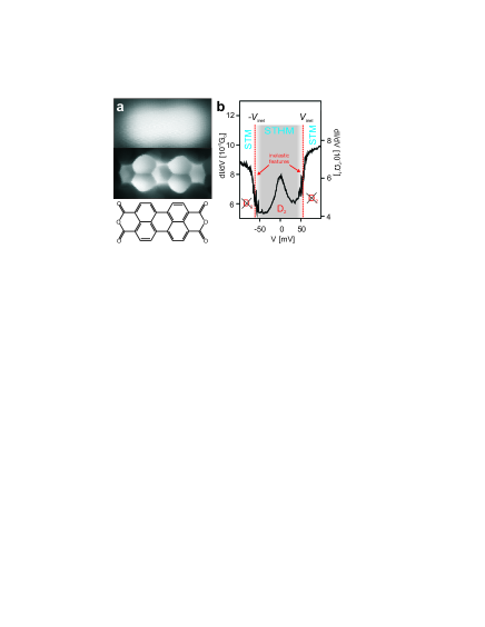
We start by summarizing the features of STHM that have been reported before 7 . The best STHM resolution (as shown in Fig. 1a) is achieved in constant-height mode with rather low tunneling bias mV. The appearance of STHM imaging after D2 dosing coincides with the emergence of non-linear differential conductance spectra close to zero bias. In particular, inelastic features appear (in Fig. 1b at ) 7 ; 8 ; 9 ; 10 . In some cases, as in Fig. 1b, a pronounced zero bias anomaly has also been observed 7 . Imaging in the presence of D2 can be switched reversibly between the STM and STHM modes by changing the applied bias 7 : If exceeds , the junction images in the conventional STM (or LDOS) mode. If, however, is sufficiently smaller than , the junction operates in the STHM mode, yielding images with ultra-high geometric resolution. The nature of the inelastic features has been investigated in detail in nanojunctions containing H2 7 ; 8 ; 9 ; 10 ; 11 . They are assigned to transitions between two structurally different states of the junction. However, the precise nature of the associated two-level system is still debated 8 ; 9 ; 10 .
Understanding the structure of the STHM junction is vital for identifying the imaging mechanism. Based on the conductance values in our experiments () we conclude that the tip-surface separation must be smaller than 1 nm 22 . At such distances the junction can accommodate only a single monolayer of D2 20 ; 14 . Clearly, the deuterium-induced imaging mode requires the presence of D2 just below the tunneling tip apex. Given the high resolution that is achieved in STHM, which in Fig. 1a is of the order 50 pm, at most one D2 molecule can be in the active area of the junction. Therefore we can model the junction in the STHM mode, i.e. at , by a single D2 molecule physisorbed 19 between the tip apex and the sample surface. For , the D2 molecule is displaced away from the tip apex, as proven by the recurrence of conventional STM imaging in conjunction with the occurrence of a structural transition at .
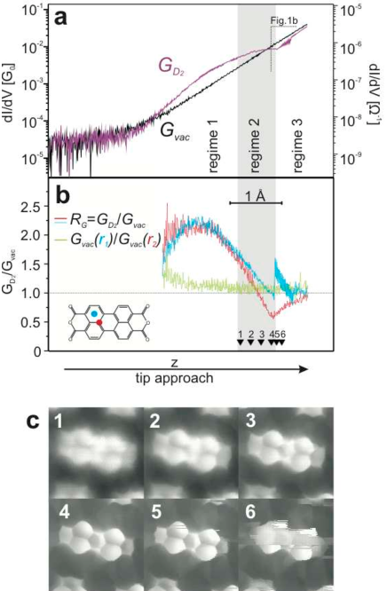
Switching the bias between and we can study the properties of a given junction, and in particular the differential conductance as a function of tip-surface distance , in presence and absence of the confined D2 molecule, without any other structural changes of the junction. Fig. 2a displays the results of -spectroscopy for the empty junction (curve measured with and labelled ) and for the junction with D2 (curve measured with and labelled ). increases exponentially with decreasing , as expected for vacuum tunneling. In contrast, behaves non-exponentially. Two opposing tendencies are observed: For intermediate , exceeds , while for smaller tip-surface distances the situation reverses. Based on the data in Fig. 2a, we can define three characteristic regimes.
At the shortest distances recorded in Fig. 2a (regime 3) exhibits increased noise and conductance jumps. Such conductance changes usually occur when the tunneling junction undergoes structural modifications due to the tip contacting the sample surface. Notably, the discontinuities in occur at tip-surface distances where still behaves strictly exponentially, i.e. the empty junction is still out of contact. Hence, the contact in question must occur via the confined D2 molecule. Clearly, the associated structural changes will occur in the softest part of the junction, i.e. the D2 molecule, which eventually is squeezed out of the junction. Indeed, images measured at the onset of regime 3 (images 5 and 6 in Fig. 2c) show a sudden loss of STHM resolution.
Having identified regime 3 with the squeezing of the D2 molecule out of the junction, we can associate the preceding regime 2 with the gradual compression of the junction that eventually causes this squeeze-out. To quantify the effect of D2 on the junction conductance in regimes 1 and 2, we define the conductance ratio . As can be seen in Fig. 2a, can be larger or smaller than 1, depending on the value of . Fig. 2b (red, blue) shows that in regime 2, where the best STHM resolution is recorded (images 3 to 5 in Fig. 2c), curves measured at different lateral positions above the PTCDA molecule each display a distinct slope. At the same time curves do not vary appreciably from point to point above PTCDA (Fig. 2b, green), which is consistent with the blurred and featureless STM images that are recorded with the empty junction at (Fig. 1a). The curves in Fig. 2b hence show that the STHM contrast in Fig. 1a can be ascribed to the effect of D2 on the junction conductance which becomes pronounced in a narrow range of -values in regime 2. We therefore need to study the nature of regime 2 in more detail.
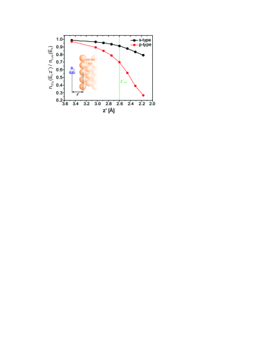
To investigate the influence of D2 on the tunnelling conductance of an STHM junction in regime 2, we have carried out a density functional theory (DFT) calculation in which we systematically varied the distance between D2 and an Au(111) surface (Fig. 3 inset) calculationdetails . This surface was chosen to model the tip electrode in our STHM experiments. We calculate the model tip DOS at the Fermi level, , as the LDOS at the metal atom located directly underneath the D2. Dividing by , the LDOS of the bare tip without D2, we find that the tip DOS decays substantially with decreasing (Fig. 3). The origin of this behavior is the Pauli exclusion principle: To minimize overlap between the closed shell of D2 and the metal electrons, both of their wave functions must rearrange locally, which depletes the metal’s local DOS in the vicinity of the Fermi level 12 ; 13 ; 14 , while the associated energy cost leads to a repulsive force between D2 and the metal (Pauli repulsion).
In the limit of low tunneling bias Tersoff-Hamann theory of STM predicts , where is the sample LDOS at tip position 17 . Accordingly, and must decrease proportionally to as D2 approaches the tip. DFT results shown in Fig. 3 suggest that the rate of tip DOS decrease should be in the range from 0.2 to 1 . At the same time experimental data from Fig. 2b show rates between 1.1 and 1.5 Å-1. To be able to compare both results we additionally have to divide experimental values by the factor accounting for the differences between the scales and . must be in the range between (soft sample) to 1 (hard wall sample). Given the effects of the unknown tip shape and the neglect of modifications of the sample LDOS by Pauli repulsion yy , the agreement between experiment and simulation is remarkable and we can thus conclude that the -variation of in regime 2 can be explained as an effect of Pauli repulsion in the STHM junction.
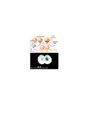
This result holds the key for understanding the contrast formation in STHM. To demonstrate this, we first discuss the STHM contrast above an inherently simple object, namely Au adatoms on Au(111), before turning to the more complex PTCDA molecule with its internal structure. Fig. 4 (bottom panel) shows the experimental image of an Au adatom dimer. The image has been recorded at constant height, nearly zero bias voltage (2 mV), and with a junction containing D2, i.e. under STHM conditions. We observe two well-separated structures, each of which corresponds to one of the adatoms. In comparison to the flat sample surface, the adatoms appear bright, i.e. with a large , because the sample LDOS at tip positions close to the adatoms, e.g. at , is increased with respect to the one at , due to a reduced effective tip-sample distance (cf. the top panel of Fig. 4). So far this is not different from conventional constant height imaging in STM. However, in the center of each of the adatoms (i.e. at ) a dark area is observed in Fig. 4. In contradiction to conventional STM bbb , Fig. 4 clearly implies that . The reason for this deviation from the normal STM behavior can be found in the presence of D2 in the junction, and in particular in its trajectory, which is displayed schematically in Fig. 4 (top): As the tip moves from to , the D2 molecule will have to move to a new vertical equilibrium position closer to the tip (smaller ) because at that position the stronger Pauli repulsion from the adatom is balanced by a stronger Pauli repulsion from the tip. In conjunction with Fig. 3, this must lead to a sharp reduction in . According to Fig. 4 this reduction overcompensates the rise in yy and leads to the dark areas in the centers of the adatoms. The analysis of the adatom image thus shows that the STHM contrast can be understood as an -map of the short-range Pauli repulsion from the sample surface acting on the D2 molecule in the STHM junction, superimposed over the conventional LDOS contrast.
With this knowledge, we can finally analyze the STHM contrast generation above PTCDA. As in the case of the dimer, the D2 molecule follows the tip and probes lateral variations of the Pauli repulsion from the adsorbed PTCDA. For example, when the tip moves from a position above the center of a C6 ring to a position directly above a carbon atom, the D2 molecule in the junction will—similarly to the trajectory shown in Fig. 4—move to a higher equilibrium position closer to the tip, because of the increased TED above the carbon atom. As in the case of the adatoms discussed above, this leads to a reduced and therefore lower conductance. In the STHM image the carbon atoms of PTCDA (and by a similar argument the -bonds between the carbons) therefore appear darker than the ”empty” spaces inside the C6 and C5O rings of the PTCDA backbone, just as observed in the image of Fig. 1a.
In conclusion, we arrive at the following model of STHM imaging: A single D2 molecule is physisorbed in the STM junction, such that it is confined directly underneath the tip apex. This molecule is the crucial element in the STHM imaging process, as it probes the short-range Pauli repulsion from the surface (sensor action) and transforms this force signal into variations of the tunneling conductance (transducer action), the latter again via Pauli repulsion. Because of its nanoscale size, the sensor is insensitive to long-range forces. Clearly, the sensor/transducer modulates the tunneling conductance on top of the normal LDOS contrast. As long as the Pauli-induced conductance modulation is larger than the LDOS-induced change of the background conductance itself, the image will be dominated by the STHM contrast. We note that the described functionality should also work with other closed-shell particles besides hydrogen and deuterium EiglerXe . Comparing STHM to conventional STM, direct tunneling between tip and sample surface still forms the basis of imaging in STHM. However, in STHM a compliant element that is sensitive to a laterally varying sample property other than the LDOS is added to the tunneling junction, where it modulates the tunneling current that is used for imaging.
Financial support from the Helmholtz Gemeinschaft is gratefully acknowledged, as are helpful discussions with J. Kroha (Bonn), S. Blügel and N. Atodiresei (Jülich).
References
- (1) C.J. Chen, Oxford University Press, (1993)
- (2) C.D. MacPherson, Phys. Rev. Lett. 77 69 (1996)
- (3) L. Bartels et al., Appl. Phys. Lett. 71 213 (1997)
- (4) A.J. Heinrich et al., Science 298 1381 (2002)
- (5) J. Repp et al., Phys. Rev. Lett. 94 026803 (2005)
- (6) W.H. Soe et al., Phys. Rev. Lett. 102 176102 (2009)
- (7) L. Gross et al., Science 325 1110 (2009)
- (8) R. Temirov et al., New J. Phys. 10 053012 (2008)
- (9) W.H.A. Thijssen et al., Phys. Rev. Lett. 97 226806 (2006)
- (10) J.A. Gupta et al., Phys. Rev. B 71 115416 (2005)
- (11) A. Halbritter et al., Phys. Rev. B 77 075402 (2008)
- (12) M.L. Trouwborst et al., Phys. Rev. B 80, 081407(R) (2009)
- (13) At contact, which corresponds to atom-atom distances of approximately 3 Å, typical conductances are of the order G0. For a typical metal, the tunneling current decays by a factor of 7.4 per Ångström 1 . For our minimum conductance of this yields a maximum distance of 8 Å.
- (14) The typical adsorption height of H2 is 3.2 Å 16 , and a typical hydrogen-hydrogen distance (for the condensed bulk) is 3.3 Å [I.F. Silvera, Rev. Mod. Phys. 52, 393 (1980)]. Two monolayers in the junction would thus require a tip-surface distance nm.
- (15) R.J.P. Keijsers et al., Phys. Rev. Lett. 76 1138 (1996)
- (16) S. Hamel and M. Cote J Chem Phys. 121 12618 (2004)
- (17) Y.G. Ptushinskii, Low Temp. Phys. 30 1 (2004)
- (18) Geometry optimization for D2 on Au(111) was done in a overlayer on a 3-layer slab within the local density approximation, yielding an upright D2 molecule in an on-top position with an equilibrium distance . For the LDOS calculation, D2 molecules in this adsorption geometry, but in a overlayer with an 11-layer slab for better convergence, were moved in steps of towards and away from the surface. For each configuration, the LDOS was calculated by projecting the quantum mechanical states on the local orbitals (, , ) of the Au atom directly below the D2. The -orbital does not yield a significant contribution. Note that DFT does not consider the masses of the nuclei (unless dynamics of the nuclei is considered), i.e. in DFT there is no difference between H2 and D2.
- (19) N.D. Lang, Phys. Rev. Lett. 46 842 (1981)
- (20) N.D. Lang, Phys. Rev. Lett. 56 1164 (1986)
- (21) J. Tersoff, D. R. Hamann, Phys. Rev. Lett. 50 1998 (1983)
- (22) For simplicity, we have neglected here the influence of D2 on . This would further amplify the variation of .
- (23) M. Ziegler et al., Phys. Rev. B 80 125402 (2009)
- (24) A. Yazdani, D.M. Eigler, N. D. Lang, Science 272, 1921 (1996)