Emergence of current branches in a series array of negative differential resistance circuit elements
Abstract
We study a series array of nonlinear electrical circuit elements that possess negative differential resistance and find that heterogeneity in the element properties leads to the presence of multiple branches in current-voltage curves and a non-uniform distribution of voltages across the elements. An inhomogeneity parameter is introduced to characterize the extent to which the individual element voltages deviate from one another, and it is found to be strongly dependent on the rate of change of applied voltage. Analytical expressions are derived for the dependence of on voltage ramping rate in the limit of fast ramping and are confirmed by direct numerical simulation.
pacs:
72.20.Ht, 84.30.-rNegative differential resistance (NDR) - in which an increasing applied voltage causes a reduced electrical current flow - occurs in a number of electronic transport systems, for example, tunnel diodes,Esaki58 semiconductor double barrier quantum well structures,Goldman87 and molecular bridges. Reed99 ; RLiu06 When several such elements are placed in a series array, forming a complex system, the NDR of individual elements often leads to striking self-organization effects associated with a spatially non-uniform distribution of electric field, despite the fact that the elements are almost identical. An important example of this behavior is provided by semiconductor superlattices consisting of a series array of quantum wells (e.g., composed of GaAs) separated by potential barriers (e.g., composed of AlAs). In the case of doped superlattices with relatively wide barrier layers (i.e., weakly-coupled superlattices), one may observe multiple current branches in current-voltage () characteristics with the number of branches approximately equal to the number of periods of the superlattice. Choi88 ; Grahn91 These branches are associated with a static, non-uniform electric field configuration in which some periods of the structure are in a low-field domain and the others in a high-field domain.SLReview ; Schoell2001 Current branching and/or non-uniform electric field distributions have been reported for other spatially-periodic systems such as quantum cascade laser structures, LuS06 multiple-quantum well infrared detectors, SchneiderS06 Si nanocrystal structures, Chen07 and two-dimensional transport in laterally patterned GaAs quantum wellsPan08 . It is remarkable that, despite the microscopic differences between these systems, the observed behavior is similar. This naturally raises two questions: What are the minimal ingredients needed to observe current branch formation? What is the role of heterogeneity in the individual element properties on this behavior?
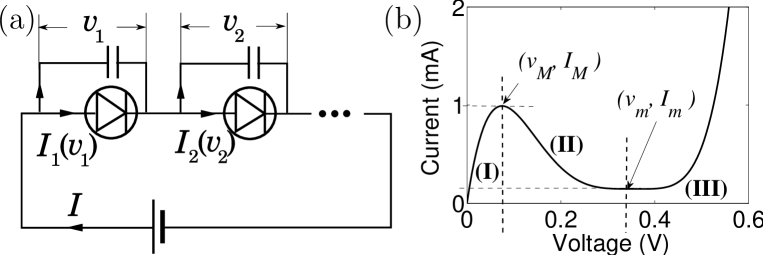
In this paper, we address these questions by introducing a nonlinear circuit model consisting of a voltage-biased series array of ideal negative differential resistance elements, each connected in parallel to a capacitance as shown in Fig. 1a. We find that heterogeneity in the element properties leads to the formation of multiple branches in current-voltage curves and a non-uniform distribution of voltages across individual elements.
The model is defined as follows. Each element of the series array is assumed to have an intrinsic curve of the form with a typical example shown in Fig. 1b. footnote1 The total electrical current is
| (1) |
for , where denotes the voltage across the -th element and is the parallel capacitance associated with the -th element. The total applied voltage to the array is . Dividing both sides of Eq. (1) by and summing over allows to express the total current as
| (2) |
where denotes the inverse total equivalent series capacitance. Relabeling the summation in Eq. (2) as over and substituting the result back into Eq. (1), the circuit model equations can be written in the following form:
| (3) |
where . Equation (3) has the form of an -dimensional dynamical system subject to a constraint on the total voltage. The constraint is built into the structure of the model, as seen by summing Eq. (3) over all and using the symmetry property . The structure of Eq. (3) is equivalent to a limiting case of a standard rate equation model for superlattices, when the doping level in each quantum well is very large. SLReview ; XuT07 ; Xu2010
In this paper, we focus on the case of linear ramping (with ramp time ) in the total applied voltage , so that increases linearly between values and and . The first term in Eq. (3) describes the effect of changing total applied voltage, while the second term describes a global coupling between individual circuit elements. When the ramping rate is large, the effect of the coupling term is expected to be small. On the other hand, when the ramping rate is small, the coupling term plays a decisive role in the observed behavior. The coupling term displays either positive or negative feedback depending on the state of each element. Considering pairs of elements, they attract one another when both are on a stable branch of the curve (i.e., Regions I and III in Fig. 1b), and repel if they are both on the unstable part (Region II). If one element is in a stable region and the other is in the unstable region, the elements may either attract or repel depending on their relative current values.
If the coupling term in Eq. (3) is neglected, one finds an uncoupled state in which the element voltages increase independently. Starting from the initial condition for all , typical for experimental measurements, SLReview ; LuS06 ; Pan08 the voltage of each element is given by . Since the are assumed to have a small dispersion, the uncoupled state is associated with a field profile that is nearly uniform. (Here, we use the term field to refer to the spatial distribution of element voltages.) When the coupling term is nonzero, the system deviates from the uncoupled state and the field profile becomes non-uniform. This behavior is usefully characterized by introducing a field inhomogeneity parameter defined by:
| (4) |
where
| (5) |
The quantity expresses the time-dependent level of field nonuniformity in the system for ramp time , while gives the maximal degree of nonuniformity during the entire ramping process and associates a single value to the entire process. For the uncoupled state, tends to zero; however, when the effect of the coupling term is large, assumes a value of order 1.
If the total voltage is held constant, the system always relaxes to a state in which the currents in the different elements are identical. This corresponds to a stable fixed point of the system with . If the average applied voltage, , falls in the NDR region of the single element curve, there are multiple fixed points corresponding to distinct arrangements of individual element voltages. For a completely homogeneous system, such that all elements are identical, i.e., and for all , these fixed points are degenerate corresponding to the same overall device current. Neu08 When the homogeneous system is subjected to a ramped voltage, starting from the initial state for all , the element voltages remain identical throughout the ramp process, i.e., , and the overall curve has a similar shape to that of a single element IC .
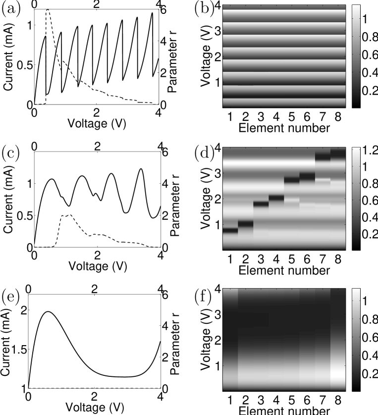
When heterogeneity is introduced into the system, current branches emerge in the limit of slow ramping as shown in the curve of Fig. 2a. The variance in the individual element characteristics is expressed as , where the ’s are independent and identically distributed (i.i.d.) random numbers, distributed normally with mean zero and standard deviation , i.e., . footnote2 We have also explored the effect of capacitance variation and variation due to electrical noise in individual elements, and find that the qualitative behavior is the same as that observed when the only variance is in the element curves. XuT08
When the ramp time is large, the system exhibits well-defined current branches in the static curves, shown in Fig. 2a for . As the total voltage ramps higher, the elements pass very rapidly from Region I to III one by one, and the current exhibits an abrupt step down for each such passage.smallN The parameter takes a value of order 1, indicative of a non-uniform distribution of element voltages. Figure 2b shows the corresponding contour plot in which the current level is plotted in gray scale vs. element number and total voltage . The clear horizontal bands indicate that, for all parts of the ramping process, the individual device currents are identical to one another.
As the ramp time decreases, the element current levels become somewhat different from one another, see Fig. 2c. In this case, more than one element can jump to Region III at the same time. The field distribution deviates less from the uniform state, the current branches are rounded and smaller in number and amplitude, and the abrupt jumps between current branches disappear. A similar rounding of experimental current branches versus ramping rate has been reported in weakly-coupled GaAs/AlAs semiconductor superlattices.RogoziaT02 The value also decreases from its large value. Figure 2d shows the corresponding current contour plot in which the horizontal bands are still evident, but interrupted by localized dark areas that correspond to the passage of individual or pairs of elements through Region II.
For fast ramping, the element currents are essentially independent of one another, and the element voltages pass through the NDR region simultaneously (Fig. 2e). The parameter approaches zero, implying that the system behavior is very close to the uncoupled state described previously. The curve of the full array follows closely that of an individual element, . The contour plot, Fig. 2f, shows smooth behavior and horizontal features are absent. We have also considered ramping from different initial states XuT08 as well as more elaborate circuit array models - e.g., including small series inductance and parallel capacitance with each nonlinear element Brown09 - and find a qualitatively similar behavior as described above.
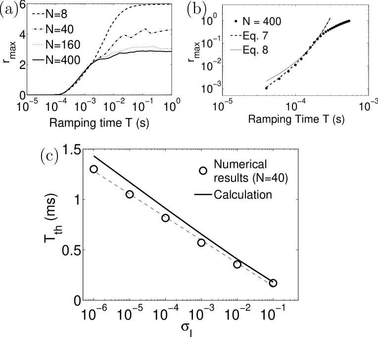
Plotting the value of versus ramp time for several different values in Fig. 3a indicates that the transition from uncoupled to fully coupled behavior is a smooth transition with an onset that is independent of system size . For large ramp time, approaches an asymptotic value that is -dependent. As , , a value that depends only on the shape of the single element function . XuT08 For the parameters used here (i.e., nF and ), the transition from uncoupled to coupled behavior occurs as the ramp time increases from 100 s to 10 ms, a timescale range that is significantly greater than the zero-bias characteristic time constant associated with an individual element, i.e., s.
To better understand this behavior, we investigate the effect of perturbations about the uncoupled state of the form
where denotes the uncoupled state solution. Substituting this form into the dynamical model, Eq. (3), one finds the following system of differential equations valid to first order in the ’s,
| (6) |
where . Equation (6) can be solved explicitly to yield the following expression for :
| (7) |
with the initial conditions for all .
For large values of ramping rate , the two exponentials in Eq. (7) are approximated by unity, and it immediately follows that
Substituting this result into the definition of , cf. Eqs. (4) and (5), allows us to write
which demonstrates that is proportional to with a coefficient of proportionality that is independent of ; this is confirmed in Fig. 3a.
For somewhat smaller values, and provided the local maximum of the element curve is sufficiently sharp, Eq. (7) can be evaluated using a saddle point method to write , where . Inserting this result back into the definition of , cf. Eq. (5), gives
In the preceding equation, we note that the exponential term takes a maximum value if we set , so that , where and are the voltage and current coordinates of the local minimum in the element characteristic, cf. Fig. 1b. This allows us to write the maximum value of over the entire ramp process as
| (8) |
Figure 3b plots the values of calculated from both Eqs. (7) and (8) and compares them with the numerical results for , demonstrating that there is a range of ramp times (around seconds) for which the asymptotic expression, Eq. (8) follows closely the transition from uncoupled to coupled behavior. In order to develop an analytic criterion for the onset of coupled behavior - and associated field non-uniformity, we define a characteristic value of ramp time that sits in this range. Denoting the corresponding characteristic value of by , we have . Solving for , we can write
| (9) |
where is slowly varying. Equation (9) shows explicitly the dependences of on element heterogeneity (i.e., ) as well as the single element NDR behavior. Interestingly, the pre-factor of the term, calculated to be s, has the form of an time with an effective resistance that depends only on the total current drop across the NDR region, . In particular, this time scale is not sensitive to the shape details of the curve in the NDR region. Figure 3c plots versus the variance level (with the specific choice ) and shows good agreement with numerical data for .
We have introduced a simple model that reveals how negative differential resistance and element heterogeneity are key sources for the observation of non-uniform field distributions and multiple current branches in the electrical conduction properties of a series array of nonlinear circuit elements. Specifically, we have shown how the system approaches a state in which the element current levels are fully coupled as the element variance level and voltage ramp rate are varied. The numerical and analytical results obtained from this model provide insight for understanding similar observed behaviors that are found for a range of more complex electronic systems, for example, semiconductor superlattices and quantum cascade laser structures. SLReview ; LuS06 ; Schoell2001 In practical devices it is often desirable to have an electric field distribution that is as spatially uniform as possible. The model introduced here points out the relevance of two factors for achieving such field distributions. One of these factors is the effective level of element heterogeneity in a periodic structure, which, in a device such as a superlattice, is determined in part by the fabricated sample quality and the electrical noise level. The second factor suggests the possible use of a time-dependent voltage bias that possesses a ramping rate through the NDR region of the device that is large enough to maintain a nearly uniform field distribution.
We gratefully acknowledge helpful conversations with Luis Bonilla, Gleb Finkelstein, Eckehard Schöll, and Adrienne Stiff-Roberts. This work was supported by the National Science Foundation through Grant No. DMR-0804232.
References
- (1) L. Esaki, Phys. Rev. 109, 603 (1958).
- (2) V. J. Goldman, D. C. Tsui, and J. E. Cunningham, Phys. Rev. Lett. 58, 1256 (1987).
- (3) J. Chen, M. A. Reed, A. M. Rawlett, J. M. Tour, Science 286, 1550 (1999).
- (4) R. Liu, S.-H. Ke, H. U. Baranger, and W. Yang, J. Am. Chem. Soc. 128, 6274 (2006).
- (5) K. K. Choi, B. F. Levine, N. Jarosik, J. Walker, and R. Malik, Phys. Rev. B 38, 12362 (1988).
- (6) H. T. Grahn, R. J. Haug, W. Müller, and K. Ploog, Phys. Rev. Lett. 67, 1618 (1991).
- (7) L. L. Bonilla and H. T. Grahn, Rep. Prog. Phys 68, 577 (2005).
- (8) E. Schöll, Nonlinear spatio-temporal dynamics and chaos in semiconductors (Cambridge University Press, Cambridge, 2001).
- (9) S. L. Lu, L. Schrottke, S. W. Teitsworth, R. Hey, and H. T. Grahn, Phys. Rev. B 73, 033311 (2006).
- (10) H. Schneider, C. Schönbein, R. Rehm, M. Walther, and P. Koidl, Appl. Phys. Lett. 88, 051114 (2006).
- (11) J. Chen, J. J. Lu, W. Pan, K. Zhang, X. Y. Chen, and W. Z. Shen, Nanotech. 18, 015203 (2007).
- (12) W. Pan, S. K. Luo, J. L. Reno, J. A. Simmons, D. Li, S. K. J. Brueck, Appl. Phys. Lett. 92, 052104 (2008).
- (13) For specificity, we use for the function a fifth-order polynomial fit to the measured curve of a tunnel diode (model 1N3712).
- (14) Huidong Xu and Stephen Teitsworth, Phys. Rev. B 76, 235302 (2007).
- (15) Huidong Xu, Ph.D. thesis, Duke University (2010).
- (16) J. C. Neu, private communication.
- (17) By contrast, the use of non-uniform initial conditions has an equivalent effect as introducing element heterogeneity to the system.
- (18) We use a Gaussian distribution on [-1,1] and have found that the observed behavior is not sensitive to the detailed form of distribution.
- (19) Huidong Xu and Stephen Teitsworth (unpublished).
- (20) For very small , one may observe smooth current branches that do not end in discontinuous current jumps, even in the static limit . Using Eq. (3) with the first term set to zero, one may estimate the minimum number of elements necessary for the first branch to end in an abrupt current jump, namely, , where denotes the magnitude of the maximal negative differential conductance in Region II of Fig. and denotes the positive differential conductance in Region I, evaluated at the same current level as . Similar conditions may be derived for each of the separate current branches.
- (21) M. Rogozia, S. Teitsworth, H. Grahn, and K. Ploog, Phys. Rev. B 65, 205303 (2002).
- (22) Kevin Brown and Stephen Teitsworth (unpublished).