Dynamical Coulomb Blockade Observed in Nano-Sized Electrical Contacts
Abstract
Electrical contacts between nano-engineered systems are expected to constitute the basic building blocks of future nano-scale electronics. However, the accurate characterization and understanding of electrical contacts at the nano-scale is an experimentally challenging task. Here we employ low-temperature scanning tunneling spectroscopy to investigate the conductance of individual nano-contacts formed between flat Pb islands and their supporting substrates. We observe a suppression of the differential tunnel conductance at small bias voltages due to dynamical Coulomb blockade effects. The differential conductance spectra allow us to determine the capacitances and resistances of the electrical contacts which depend systematically on the island–substrate contact area. Calculations based on the theory of environmentally assisted tunneling agree well with the measurements.
pacs:
73.63.-b, 73.40.-c, 73.23.Hk, 73.40.JnIntroduction.— The detailed understanding and precise engineering of electrical contacts between nano-sized metallic objects and their supporting substrates are not only of fundamental interest; they are also of crucial importance for the development of future electronics. As the nano-scale is approached, localization of charges in small regions of a device plays an increasingly important role and charging effects start to dominate the electron transport. Size reduction may for example lead to a change of the magnetic Seneor et al. (2007) or superconducting Bose et al. (2010) properties of a sub-micron contact. Investigations of electrical contacts in nano-scale systems are thus called for to help predict, design, and understand the functionality of nano-devices and thereby facilitate further progress in the fabrication of nano-scale electrical circuits Lu and Lieber (2006); Likharev (2003).
One prominent charging mechanism is the dynamical Coulomb blockade (DCB) effect by which single electrons tunneling through a barrier exchange energy with the electromagnetic environment. These inelastic processes leave clear fingerprints in the current–voltage characteristics of a device and contain detailed information about the impedance of the electrical circuit in which the tunnel barrier is embedded. The DCB effect was discussed theoretically in seminal works by Devoret et al. Devoret et al (1990), Girvin et al. Girvin et al. (1990), and Ingold and Nazarov Ingold and Nazarov (1992). Experimentally, it was observed in systems that were carefully engineered in order to obtain a high-impedance environment close to the tunnel barrier Cleland et al. (1992); Holst et al. (1994); Joyez et al. (1997); Zheng et al. (1998); Pierre et al. (2001); Pekola et al. (2010); Saira et al. (2010); Parmentier et al. (2011). The DCB effect, however, is not just an interesting physical phenomenon, it also leads to practical applications as we demonstrate below.

In this Letter we make use of DCB as a means to probe and characterize the electrical contact between flat metallic nano-scale islands and their supporting substrates. We employ low-temperature scanning tunneling spectroscopy to measure the electrical conductance of individual Pb islands on metallic, semimetallic, semiconducting, and partially insulating substrates. At low voltages we observe a suppression of the differential tunnel conductance due to DCB. Importantly, the tunnel current between the scanning tunneling microscope (STM) and the flat islands is highly sensitive to the impedance of the electrical contact between the island and the supporting substrate. This in turn allows us to investigate the nano-sized electrical contacts, employing the theory of DCB, and thereby extract the resistances and capacitances of the island–substrate contacts from the measured differential conductance spectra.
Experiment.— Figure 1 shows STM images of Pb(111) islands grown on substrates of Cu(111), Si(111)-77, highly oriented pyrolytic graphite (HOPG), hexagonal (h-)BN/Ni(111), and NaCl/Ag(111). The island areas range from 10 nm2 to 10nm2 with island heights between 2 and 60 monolayers (ML). The substrate crystals were prepared according to standard procedures: The h-BN ML was epitaxially grown on Ni(111) Nagashima et al. (1995). The Si(111) crystal was heavily -doped and prepared to form a Si(111)-77 reconstruction. NaCl was thermally evaporated onto Ag(111) at substrate temperatures between 300 K and 500 K Repp et al. (1995). The flat islands were grown by evaporation of Pb from a W filament onto the substrates whose temperatures were stabilized between 130 K and 300 K to control the island sizes. We chose Pb as a typical metallic material because of the well-known growth of Pb films or islands on Si(111) Jalochowski et al. (1988); Weitering et al. (1992), Cu(111) Hinch et al. (1989), and HOPG Dil et al. (2007). On HOPG, h-BN/Ni(111), and NaCl islands grow directly on top of the substrates, whereas on Si(111) and Cu(111) a 1 ML wetting layer forms first followed by the growth of single-crystal Pb islands Feng et al. (2004).
Conduction measurements were performed in a home-built STM with PtIr tips operated under ultra-high vacuum at a temperature of K Gaisch et al. (1992). We focused exclusively on islands supported by just a single substrate terrace such that the electrical contact between the island and the substrate was essentially uniform across the whole contact area. The differential conductance was measured in an open feedback loop using a lock-in technique with a peak–to–peak modulation voltage between mV and mV using a typical current of 1 nA and voltage ranges between mV and mV. We verified experimentally that the conductance spectra are independent of the injected power in a range between and W.
Figure 2 displays a selection of differential conductance spectra measured on individual Pb islands of varying sizes on top of the different substrates. The experimental data are corrected for a background contribution due to quantum-well states Brun et al. (2009); Hong et al. (2009) and rescaled by the tunneling resistance between the islands and the STM tip such that the normalized spectra approach unity at large voltages. The temperature was below the critical temperature of bulk lead ( K) and one could expect the Pb islands to display superconducting properties for voltages below the superconducting gap of bulk Pb, 1.3 meV Brun et al. (2009). However, recent experiments have shown that both and decrease below their bulk values for small systems Brun et al. (2009); Liu (2011) and superconducting gap features give a negligible contribution to the conductance under our experimental conditions. On larger voltage scales the quasi-particle transport between the islands and their normal-state substrates is the same as for islands in their normal-state as we checked by performing experiments at temperatures above .
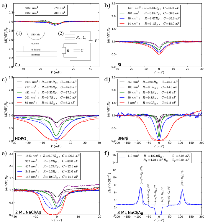
While Fig. 2a shows that the differential conductance for the islands on Cu(111) essentially remains flat independently of the island size, we observe in Figs. 2b-e a suppression of the differential conductance at low voltages which becomes increasingly prominent as the island size is decreased. We attribute the low-bias suppression to DCB due to the high-impedance electrical contact formed between the islands and the substrates. The normalized differential conductance is reduced below unity when the applied voltage is smaller than the charging energy , where is the capacitance of the system. The suppression (and the charging energy) increases as the islands become smaller. For the islands on Cu(111), the electrical contact has a very low resistance such that the spectrum essentially is ohmic and in this case we ascribe the small features in the spectra to the reduced electron–phonon scattering of the quantum-well states below the Debye energy meV of Pb Wang et al. (2009); Brun et al. (2009). In Figs. 2e-f we show results for Pb islands on Ag(111) covered with 2 and 3 MLs of insulating material (NaCl) between islands and substrates. As several insulating MLs are introduced the spectra begin to display qualitatively different features as we explain below.
Theory.— To understand quantitatively the measured conductance spectra, we employ the –theory of DCB which explicitly incorporates the impedance of the electrical circuit in calculations of the current Devoret et al (1990); Girvin et al. (1990); Ingold and Nazarov (1992); Joyez and Esteve (1997). The total impedance (as seen from the tunnel junction) reads , where is the capacitance of the tunnel (tip–island) junction and is the impedance of the external circuit Ingold and Nazarov (1992). In our experiment, see inset of Fig. 2a, the impedance of the island–substrate contact is , where () is the capacitance (ohmic resistance) of the island–substrate contact, and we obtain with . The tunneling resistance M – 1 G between STM tip and island is much larger than the resistance quantum k, which justifies a perturbative calculation in the tunnel coupling. The DC current then reads
| (1) |
with . The tunneling rates are
| (2) |
where is the probability for an electron to emit the energy into the electrical circuit Ingold and Nazarov (1992). The –function can be written
| (3) |
where is the equilibrium correlation function of the phase of the voltage across the tip–island tunnel junction. It can be expressed via the total impedance as
| (4) |
which we evaluate analytically Joyez et al. (1997). Finally, we convolve the calculated current with the instrumental resolution function that accounts for the broadening due to the modulation voltage Klein et al. (1973); Li et al. (1998). The resulting current is then .
Results.— Figures 2b-e show calculations of the differential conductance based on Eqs. (1–4). The fitting parameters and used for the calculations were independently extracted from the experimental data: The charging energy is given mainly by 1 aF, which determines the width of the differential conductance suppression. The resistance determines the shape of the curves at small voltages and is adjusted so that the theoretical curves best fit the experimental data.
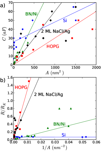
The theoretical curves are in good agreement with the experimental data and show a clear dependence of the electrical island–substrate contact on the island area. To corroborate our analysis we consider the extracted capacitances and resistances as functions of the island areas. One would expect that the capacitance (resistance) increases with the (inverse) contact area . This systematic behavior is confirmed by Fig. 3, showing that we indeed are probing the electrical contact between the islands and the substrates. For HOPG, BN/Ni(111), and 2 ML NaCl/Ag(111) the capacitance (resistance) depends approximately linearly on the (inverse) island area. For Si(111), in contrast, a different behavior is observed: the capacitance has a clear off-set value for small islands and the resistance is essentially independent of the island area. This is due to the wetting layer whose resistance (in parallel) mainly determines the current to the electrical drain contact and whose capacitance does not depend on the island size, giving rise to the off-set at .
Finally, we turn to the samples with several insulating MLs between islands and substrate, Figs. 2e-f. As additional MLs are introduced, electron transport between islands and substrate takes place by tunneling through the insulating layers. The islands are then connected both to the tip and the substrate via tunneling barriers and the orthodox theory of tunneling through a double junction applies Averin and Likharev (1991). According to our analysis this occurs with 3 or more MLs of NaCl. In Fig. 2e (2 MLs) some deviations between experiment and the theory of DCB are already visible for large islands and in Fig. 2f (3 MLs) we calculated the spectra using the orthodox theory Hanna and Tinkham (1991). The gap is associated with the island–substrate junction while the two peaks represent spectral features due to the tip–island junction. The asymmetric gaps in Figs. 2e,f are due to the fractional residual charge on the Pb islands, which shifts the spectra Hanna and Tinkham (1991). The controlled addition of single insulating MLs opens an interesting approach to systematic investigations of asymmetric double junctions, similar to recent works on nano-particles coupled to metallic electrodes Bitton et al. (2011); Xu et al. (2011).
Conclusions.— We have used DCB effects to characterize the electrical contact between metallic nano-islands and their supporting substrates in low-temperature STM measurements. Our analysis is supported by the systematic area-dependence of the capacitances and resistances. The present work facilitates quantitative investigations of electrical nano-contacts and is important for future studies of the physical and chemical properties of supported nano-structures in relation to superconductivity, magnetism, and catalysis.
Acknowledgements.— We thank J. P. Pekola for indispensable advice and M. Büttiker, T. Cren, and D. Roditchev for instructive discussions. The work was supported by the Swiss National Science Foundation.
References
- Seneor et al. (2007) P. Seneor, A. Bernand-Mantel, and F. Petroff, J. Phys. Condens. Matter 19, 165222 (2007).
- Bose et al. (2010) S. Bose et al., Nature Mater. 9, 550 (2010).
- Lu and Lieber (2006) W. Lu and C. Lieber, Nature 32, 841 (2006).
- Likharev (2003) K. K. Likharev in Nano and Giga Challenges in Microelectronics (Elsevier, Amsterdam, 2003).
- Devoret et al (1990) M. H. Devoret et al., Phys. Rev. Lett. 64, 1824 (1990).
- Girvin et al. (1990) S. M. Girvin et al., Phys. Rev. Lett. 64, 3183 (1990).
- Ingold and Nazarov (1992) G.-L. Ingold and Yu. V. Nazarov in Single Charge Tunneling (Plenum, New York, 1992).
- Cleland et al. (1992) A. N. Cleland et al., Phys. Rev. B 45, 2950 (1992).
- Holst et al. (1994) T. Holst, D. Esteve, C. Urbina, and M. H. Devoret, Phys. Rev. Lett. 73, 3455 (1994).
- Joyez et al. (1997) P. Joyez et al., Phys. Rev. Lett. 79, 1349 (1997).
- Zheng et al. (1998) W. Zheng et al., Solid State Commun. 108, 839 (1998).
- Pierre et al. (2001) F. Pierre et al., Phys. Rev. Lett. 86, 1590 (2001).
- Pekola et al. (2010) J. P. Pekola et al., Phys. Rev. Lett. 105, 026803 (2010).
- Saira et al. (2010) O.-P. Saira, M. Möttönen, V. F. Maisi, and J. P. Pekola, Phys. Rev. B 82, 155443 (2010).
- Parmentier et al. (2011) F. D. Parmentier et al., doi:10.1038/nphys209.
- Nagashima et al. (1995) A. Nagashima et al., Phys. Rev. B 51, 4606 (1995).
- Repp et al. (1995) J. Repp and G. Meyer Appl. Phys. A 85, 399 (2006).
- Jalochowski et al. (1988) M. Jalochowski et al., Phys. Rev. B 38, 5272 (1988).
- Weitering et al. (1992) H. H. Weitering et al., Phys. Rev. B 45, 5991 (1992).
- Hinch et al. (1989) B. J. Hinch et al., Europhys. Lett. 10, 341 (1989).
- Dil et al. (2007) J. H. Dil et al., Phys. Rev. B 45, 161401(R) (2007).
- Feng et al. (2004) R. Feng et al., Appl. Phys. Lett. 85, 3866 (2004).
- Gaisch et al. (1992) R. Gaisch et al., Ultramicroscopy 42, 1621 (1992).
- Brun et al. (2009) C. Brun et al., Phys. Rev. Lett. 102, 207002 (2009).
- Hong et al. (2009) I-Po Hong et al., Phys. Rev. R 80, 081409(R) (2009).
- Liu (2011) J. Liu et al., J. Phys.: Condens. Matter 23, 265007 (2011).
- Wang et al. (2009) K. Wang et al., Phys. Rev. Lett. 102, 076801 (2009).
- Joyez and Esteve (1997) P. Joyez and D. Esteve, Phys. Rev. B 56, 1848 (1997).
- Klein et al. (1973) J. Klein et al., Phys. Rev. B 7, 2336 (1973).
- Li et al. (1998) J. Li, W.-D. Schneider, R. Berndt, and S. Crampin, Phys. Rev. Lett. 81, 4464 (1998).
- Averin and Likharev (1991) D. V. Averin and K. K. Likharev, Mesoscopic Phenomena in Solids (Elsevier, Amsterdam, 1991).
- Hanna and Tinkham (1991) A. E. Hanna and M. Tinkham, Phys. Rev. B 44, 5919(R) (1991).
- Bitton et al. (2011) L. Bitton, D. B. Gutman, R. Berkovits, and A. Frydman, Phys. Rev. Lett. 106, 016803 (2011).
- Xu et al. (2011) R. Xu et al., arXiv:1106.2777 (2011).