Reduced frequency noise in superconducting resonators
Abstract
We report a reduction of the frequency noise in coplanar waveguide superconducting resonators. The reduction of 7 dB is achieved by removing the exposed dielectric substrate surface from the region with high electric fields and by using NbTiN. In a model-analysis the surface of NbTiN is found to be a negligible source of noise, experimentally supported by a comparison with NbTiN on SiOx resonators. The reduction is additive to decreasing the noise by widening the resonators.
The development of large and sensitive imaging arrays for far infrared astronomical instrumentation is rapidly progressing with microwave kinetic inductance detectors day . Arrays have already been taken to ground-based telescopes monfardini ; schlaerth , and readout using frequency domain multiplexing has been demonstrated yatesapl . The frequency noise in these superconducting resonators is two to three orders of magnitude above the fundamental limit of generation-recombination noise. The noise has been conjectured to arise from dipole two-level systems (TLS) in surface dielectrics gaoapl2007 , which is supported by recent experiments: The surface has been shown to be a dominant source of noise, by measurements on the width scaling by Gao et al. gaoapl2008-2 . Moreover, we have shown that introducing dielectrics by covering the resonators with SiOx leads to an increase in the noise barendsapl . Noroozian et al. showed that the noise arises predominantly from the capacitive portion of the resonator by using a lumped element capacitor noroozianaipconf . Noise reduction can be achieved by widening the resonator, in essence decreasing the surface to volume ratio gaoapl2008-2 ; noroozianaipconf ; barendsieee2009 . However, the practically limiting source of noise remains to be identified and reduced.
Here, we show that the noise can be decreased by minimizing the dielectrics in the resonator itself. The lowest noise is achieved by using NbTiN deposited on top of a hydrogen passivated substrate as well as by removing the substrate from the region with the largest electric fields. The combination of removing the substrate and widening the resonator leads to a reduction of 9 dB for our first-generation resonators.
Dipole TLS are known to influence the temperature dependent permittivity phillips , and consequently the resonance frequency. The superposition of permittivity and complex conductivity () controls the resonance frequency barendsapl ; gaoapl2008
| (1) |
with the kinetic inductance fraction and for the thick film and for the thin film limit. The filling factor gaoapl2008 takes into account the location of the dielectric and weighs its contribution to the frequency by the electric field energy inside our resonator geometry. It is defined by , with the capacitance per unit length, the standing wave voltage, the length of the resonator, and the relative permittivity and the volume of the dielectric hosting the TLS.
Similarly, dipole TLS cause frequency noise through the time-varying permittivity gaoapl2007 . Consequently, the power spectral density of the permittivity translates to frequency noise gaoapl2008-2 ,
| (2) |
with the normalized frequency noise.
In order to identify the contribution of the various surfaces to noise we calculate the effect of a hypothetical surface layer with thickness containing dipole TLS. The electric fields in the coplanar waveguide geometry are calculated using the potential matrix to find the charge density. The approach is detailed in Ref. barendsarxiv . We adopt the assumption by Gao et al. gaoapl2008-2 that the noise spectral density follows: , with the saturation electric field strength, following the saturation of microwave loss due to TLS at high intensities phillips .
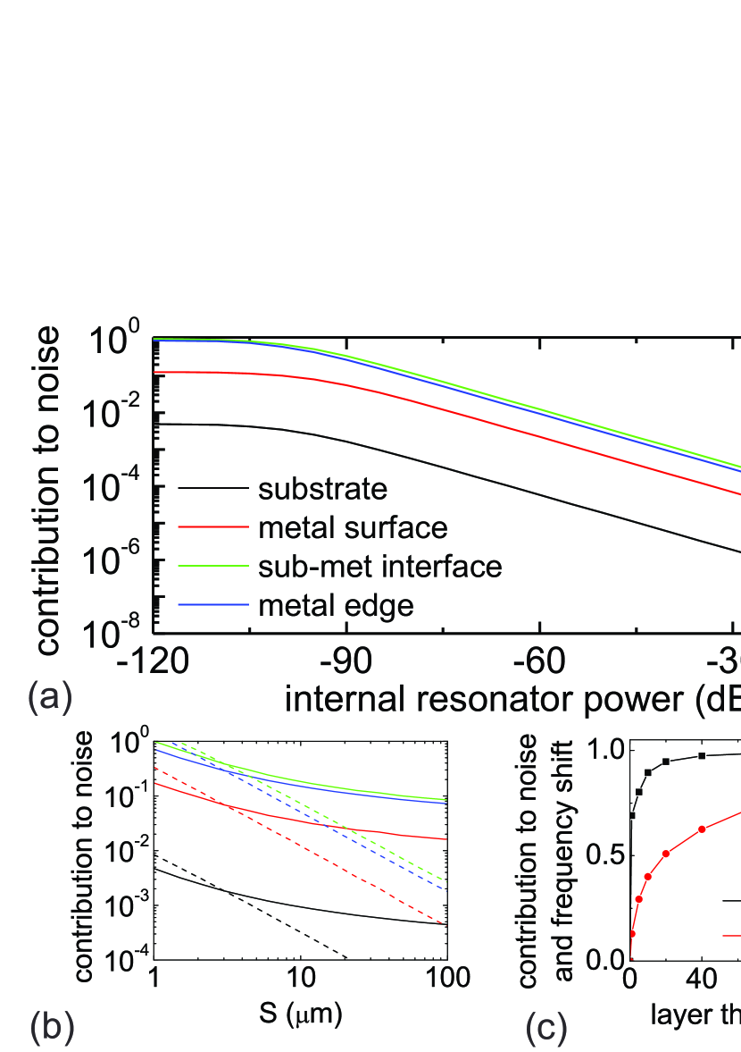
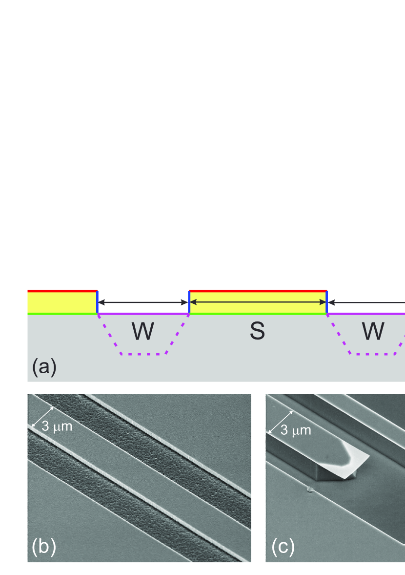
The hypothetical layer is placed along each of the outlined surfaces in Fig. 1a, the exposed substrate surface, the top metal surface, the etched metal edges and the substrate-metal interface. The results are shown in Fig. 2a-b. Importantly, the contribution to the frequency noise is about two orders of magnitude larger when the layer is placed on surfaces adjacent to the metal than when placed on the exposed substrate. This is due to the high electric fields close to the metal. Moreover, we find that the noise follows in the relevant power range, with the internal resonator power barendsthesis . In addition, when widening the resonator geometry the noise decreases. We have also calculated the influence of a metal surface dielectric with finite thickness on the noise as well as the frequency shift, i.e. Eq. 1 and Eq. 2. We find that for the noise, only the first few nanometers matter, whereas the full volume influences the frequency shift. This is consistent with our previous experiments, where we showed that frequency deviations arise from the bulk of the dielectric while noise arises predominantly at surfaces and interfaces barendsapl . The difference arises from the surface layer being weighed by for the noise and for the frequency shift. Interestingly, the power and width dependence is very similar for each of the surfaces, and identification of the dominant noise source can be done only by removing or altering a specific surface.
In order to identify and reduce the dominant noise source, we have fabricated a series of devices aimed at addressing a specific surface, see Fig. 1. We use NbTiN quarterwave coplanar waveguide resonators day ; barendsapl with varying geometry or composition. Resonance frequencies lie between 3-5 GHz. As a reference a 300 nm NbTiN film is DC sputtered on an HF-cleaned high resistivity ( kcm) -oriented Si wafer. Patterning is done using SF6/O2 reactive ion etching. The critical temperature is =14.8 K, the low temperature resistivity is =170 cm and the residual resistance ratio is 0.94. To identify the importance of using hydrogen passivated Si, a 300 nm NbTiN film has been deposited on the native oxide of Si ( K, cm and ). We have also removed the exposed substrate surface from the region with large electric fields: fully straight, 50 nm thick, NbTiN resonators are made on Si, aligned along the axis of the Si substrate ( K, cm and ). Using KOH wet etching, 0.9 m deep grooves (dashed lines in Fig. 1a) are etched in the gaps along the full length of the resonators. As a reference for the latter sample as well as to clarify the influence of the metal edges, a straight, 50 nm thick NbTiN resonator is made where the Si substrate is not removed.
The frequency noise is measured using a homodyne detection scheme based on quadrature mixing day ; barendsthesis ; barendsapl . The samples are cooled to a temperature of 310 mK using a He-3 sorption cooler placed in a 4.2 K liquid He cryostat. The sample stage is magnetically shielded with a superconducting shield. We use a low noise high electron mobility transistor amplifier with a noise temperature of 4 K wadefalk .
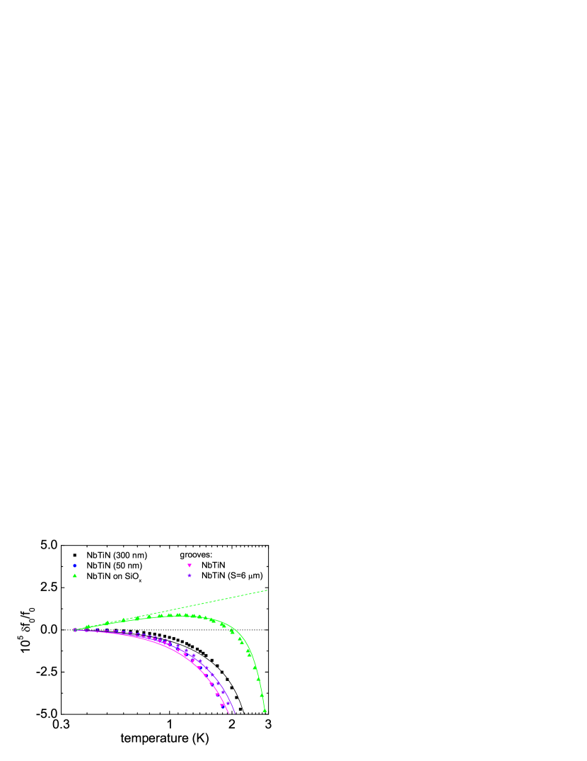
The temperature dependence of the resonance frequency is shown in Fig. 3. For the NbTiN on SiOx resonator we find a clear nonmonotonicity. The superposition (Eq. 1) of the complex conductivity and logarithmically temperature dependent permittivity describes the data. The logarithmic dependence is consistent with resonant interaction of TLS with the electric fields at phillips : with the TLS density of states, the dipole moment and an arbitrary reference temperature. The temperature dependence of the other resonators follows Mattis-Bardeen mattis , provided a broadening parameter dynes of eV is included in the density of states lambda .
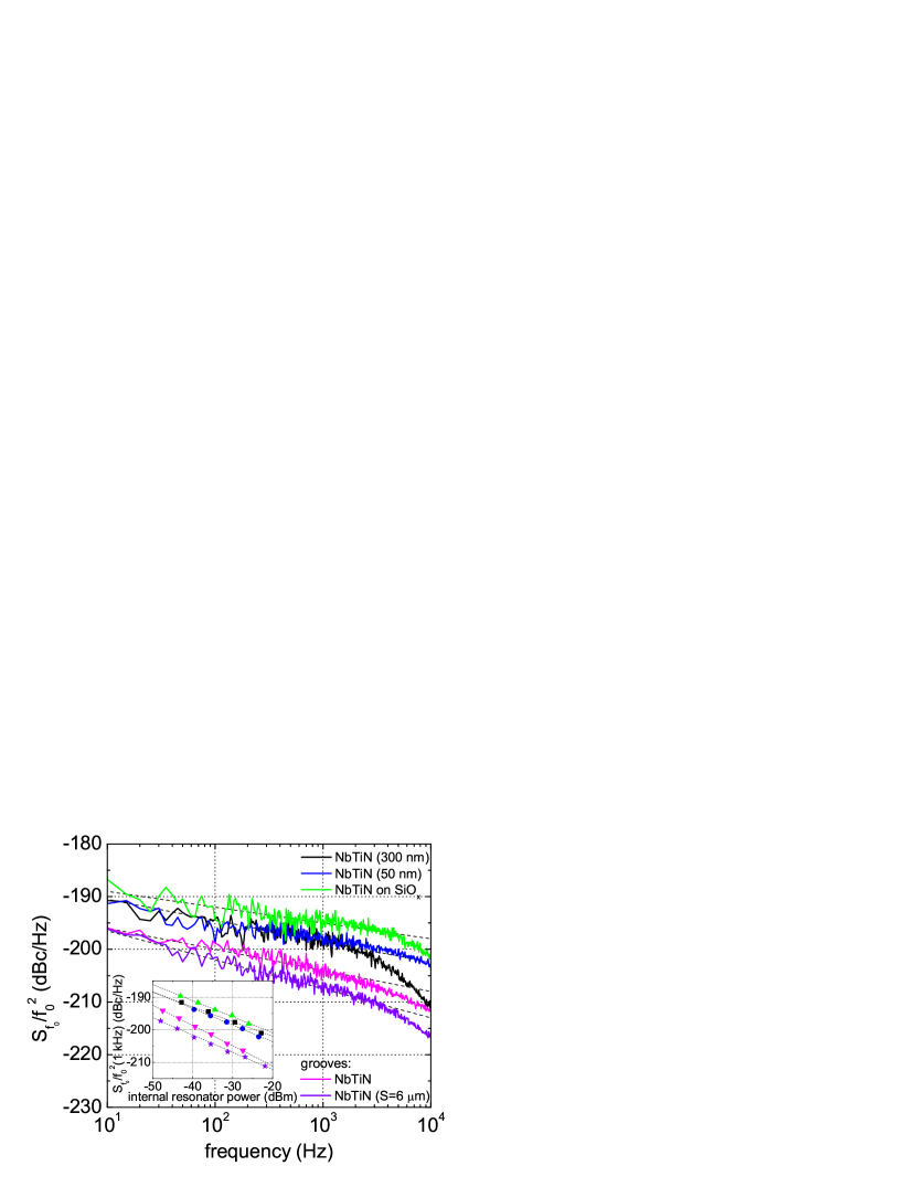
The frequency noise spectra are shown in Fig. 4. The inset shows the dependence on the internal resonator power . The noise spectra follow , until a roll-off frequency on the order of 10 kHz. This roll-off arises from the resonator-specific response time, set by the loaded quality factor and resonator frequency. The NbTiN on SiOx resonator has the highest frequency noise, at dBm: (1 kHz) dBc/Hz. This is 3 dB noisier than the standard, 300 nm thick, NbTiN resonator which has a noise level of dBc/Hz. The noise remains at dBc/Hz when decreasing the metal thickness by a factor of 6 (8 dB), from 300 nm to 50 nm. Clearly, the noise is decreased with 7 dB for the resonator with grooves in the gaps, having (1 kHz) dBc/Hz. Moreover, the noise is reduced over the whole range of spectral frequency and internal resonator power. For the wider resonator with m the noise is 2 dB lower at dBc/Hz. We find that the frequency noise follows , up to powers of dBm.
The data and analysis show that NbTiN is a clean material and point towards SiOx as the dominant source of noise. First, the exposed Si surface dominates the noise as its removal decreases the noise considerably. Second, when placing SiOx below or on top of NbTiN the noise increases (Fig. 4 and Ref. barendsapl ). Third, the analysis in Fig. 2 indicates that the NbTiN surface is clean compared to that of Si, as the metal surfaces influence the noise much stronger than the exposed substrate. In addition, the monotonic temperature dependence of the resonance frequency down to 350 mK indicates that NbTiN has a minimal dielectric layer, in contrast to Nb, Ta and Al barendsapl as well as NbTiN on SiOx. Moreover, the metal edges are not dominant, as the noise level is independent of the thickness of the metal. Finally, the removal of dielectrics from the gaps leads to a decrease in the capacitance in Eq. 2. Hence, if the metal surfaces would dominate, the noise would increase. Quantitatively, we estimate (1 kHz) 1/Hz for SiOx, assuming nm. Importantly, the noise reduction is significant: it is 7 dB below our standard NbTiN on Si resonators and 11 dB below the lowest values reported for coplanar waveguide resonators by Gao et al. gaoapl2007 . In addition, the noise is 2 dB lower when widening to m, which is consistent with our calculation (1.9 dB, see Fig. 2b) and shows that further improvements can be obtained by widening the resonator.
The data in Fig. 4 provide a clear guide to low noise superconducting resonators, by using NbTiN and removing the exposed substrate surface from the region with the largest electric fields. A particular approach to remove the dielectric was followed in Ref. mazin . Importantly, we show that both the removal of dielectrics as well as the widening of the resonator leads to a significant decrease of the noise. Hence, both approaches can be considered to be additive to decreasing the noise. Our approach can be implemented for lumped element resonators doyle ; noroozianaipconf as well: by using a -oriented Si wafer and aligning the fingers and edges of the interdigitated capacitor along the two perpendicular axes, grooves can be etched with a minimal amount of undercut. Interestingly, our resonators with grooves etched in the gaps also have higher quality factors at high internal power levels as well as at the single microwave photon levels needed for circuit quantum electrodynamics barendsarxiv .
To conclude, we have reduced the frequency noise by using NbTiN and removing the substrate from the region with the highest electric fields. This indicates that the exposed Si substrate surface is the main source of the noise, hence the contribution to noise from the NbTiN surface is not dominant. The followed approach is a straightforward route to low frequency noise in superconducting resonators.
Acknowledgements.
The authors thank J. M. Martinis for stimulating discussions. The work was supported by the Pieter Langerhuizen Lambertuszoon funds of the Royal Holland Society of Sciences and Humanities and by the EU NanoSciERA project “Nanofridge”.References
- (1) P. K. Day, H. G. LeDuc, B. A. Mazin, A. Vayonakis, and J. Zmuidzinas, Nature 425, 817 (2003).
- (2) J. Schlaerth, A. Vayonakis, P. Day, J. Glenn, J. Gao, S. Golwala, S. Kumar, H. LeDuc, B. Mazin, J. Vaillancourt, and J. Zmuidzinas, J. Low Temp. Phys. 151, 684 (2008).
- (3) A. Monfardini et al., arXiv:1004.2209.
- (4) S. J. C. Yates, A. M. Baryshev, J. J. A. Baselmans, B. Klein, and R. Güsten, Appl. Phys. Lett. 95, 042504 (2009).
- (5) J. Gao, J. Zmuidzinas, B. A. Mazin, H. G. LeDuc, and P. K. Day, Appl. Phys. Lett. 90, 102507 (2007).
- (6) J. Gao, M. Daal, J. M. Martinis, A. Vayonakis, J. Zmuidzinas, B. Sadoulet, B. A. Mazin, P. K. Day, and H. G. LeDuc, Appl. Phys. Lett. 92, 212504 (2008).
- (7) R. Barends, H. L. Hortensius, T. Zijlstra, J. J. A. Baselmans, S. J. C. Yates, J. R. Gao, and T. M. Klapwijk, Appl. Phys. Lett. 92, 223502 (2008).
- (8) O. Noroozian, J. Gao, J. Zmuidzinas, H. G. LeDuc, and B. A. Mazin, AIP Conf. Proc. 1185, 148 (2009).
- (9) R. Barends, H. L. Hortensius, T. Zijlstra, J. J. A. Baselmans, S. J. C. Yates, J. R. Gao, and T. M. Klapwijk, IEEE Trans. Appl. Sup. 19, 936 (2009).
- (10) W. A. Phillips, Rep. Prog. Phys. 50, 1657 (1987).
- (11) J. Gao, M. Daal, A. Vayonakis, S. Kumar, J. Zmuidzinas, B. Sadoulet, B. A. Mazin, P. K. Day, and H. G. LeDuc, Appl. Phys. Lett. 92, 152505 (2008).
- (12) R. Barends, N. Vercruyssen, A. Endo, P. J. de Visser, T. Zijlstra, T. M. Klapwijk, P. Diener, S. J. C. Yates, J. J. A. Baselmans, arXiv:1005.0408.
- (13) R. Barends, Ph. D. thesis, Delft University of Technology, 2009 (electronic version: repository.tudelft.nl).
- (14) N. Wadefalk et al., IEEE Trans. on Micr. Theory and Tech. 51, 1705 (2003).
- (15) D. C. Mattis and J. Bardeen, Phys. Rev. 111, 412 (1958).
- (16) R. C. Dynes, V. Narayanamurti, and J. P. Garno, Phys. Rev. Lett. 41, 1509 (1978).
- (17) For 300 nm thick NbTiN, NbTiN on SiOx, and 50 nm thick NbTiN we find for : 0.18, 0.08 and 0.33, respectively. We infer a magnetic penetration depth of 400, 240 and 270 nm.
- (18) B. A. Mazin, Ph. D. thesis, California Institute of Technology (2004).
- (19) S. Doyle, P. Mauskopf, J. Naylon, A. Porch, and C. Duncombe, J. Low Temp. Phys. 151, 530 (2008).