Effects of Parasitics and Interface Traps On Ballistic Nanowire FET In The Ultimate Quantum Capacitance Limit
Abstract
Index terms: Nanowire FET, Coupled Poisson-Schrodinger Equations, Quantum Capacitance, Ballistic Transistor, Transistor scaling, Parasitic Capacitance, Interface traps.
Index terms: Nanowire FET, Coupled Poisson-Schrodinger Equations, Quantum Capacitance, Ballistic Transistor, Transistor scaling, Parasitic Capacitance, Interface traps.
I Introduction
As we scale down the lateral as well as the longitudinal dimensions of the channel of a non-planar transistor and replace the Silicon channel by a so-called ‘high-mobility’ (or low effective mass) material, we start reaching two limits. The first limit is an electrostatic one, termed as ‘Quantum Capacitance Limit’ (QCL) [1]-[8]. The strong energy quantization due to the geometrical confinement in a multi-gated structure and the low density of states due to small effective mass of the channel material causes a small ‘quantum capacitance’ to be in series with the gate oxide capacitance . The small quantum capacitance dominating the total gate capacitance results in a number of interesting effects in the transistor characteristics [6]-[8]. There have been a number of experimental efforts as well, in a variety of systems to capture the effect of such quantum capacitance [9, 10]. The other limit, so called ‘Ballistic Transport Limit’ (BTL) is transport related which results from the scaling of the channel length and the relatively large mean free path of high mobility channel materials [11]-[14]. Scaling of multi-gate transistors thus leads to a regime where the transistor is expected to be operating in both the limits.
In this work, we analyze a Gate-All-Around nanowire transistor operating in such limiting conditions. There have been a few reports in the recent past where the performance of such a transistor has been evaluated in the QCL in an ideal condition and compared with the classical capacitance limit (CCL) where the gate oxide is dominant [8, 15, 16]. However, the effects of device non-idealities on transistor performance become extremely important in this regime. The presence of parasitic capacitance and interface traps significantly reduces the fraction of the useful (mobile) charge in the total switching charge in the strong quantum capacitance limit. On the other hand, strong energy quantization increases the relative channel resistance in this limit which in turn improves immunity of the transistor towards the source/drain series resistance. Thus, the combined effects of these non-idealities are expected to play a significant role in the transistor characteristics in the strong quantum capacitance limit and are addressed in detail in the present work.
The paper is organized as follows: we describe the simulation model used in this work in sec. II. In sec. III, we start with a formal definition of the Ultimate Quantum Capacitance Limit (UQCL), followed by a detailed analysis of the C-V characteristics of a nanowire transistor in this regime in presence of the interface traps. Sec. IV presents a comparative analysis between UQCL and CCL regime of operation on (i) the saturation of drain current and (ii) the subthreshold slope, both in the presence and absence of different device non-idealities. In the same section, we also analyze the scaling performance of the transistor in such limits. The performance benchmarking procedure that we follow in this work is based on the criteria proposed in [17]. This is followed by the discussion on the effects of the above said non-idealities on the scaling performance in sec. V. We demonstrate that the device non-idealities should be carefully taken into account for realistic performance evaluation in a nanowire transistor in the UQCL regime. Finally, we conclude the paper in sec. VI.
II A Ballistic Nanowire FET Model
Here we use a FET model, which is a variation of the ‘Top-of-the-Barrier’ model described in [12], for a gate-all-around (GAA) square nanowire of width , schematically shown in Fig. 1. We assume a parabolic bandstructure of the nanowire described by an isotropic effective mass .
First, a hypothetical nanowire FET is assumed where the top of the source to channel barrier at = is physically far off from the source and the drain eliminating any potential coupling from the source or the drain. Then, the gate voltage () governed 2-D potential profile and the carrier density profile are obtained at = plane of the hypothetical FET using coupled 2-D Schrodinger-Poisson equations:
| (1) |
and
| (2) |
Here is the energy minimum of the subband, and are the electronic charge and dielectric constant of the channel respectively. Assuming a ballistic channel, the carriers with and states are in equilibrium with the chemical potentials of the source () and the drain () respectively with . Thus,
| (3) |
where
| (4) |
is the 1D density of states (DOS) of the subband in the channel given by
| (5) |
where is a step function. are the Fermi-Dirac probabilities which, at temperature , are expressed as
| (6) |
where is the Boltzmann constant. The wavefunction is assumed to be zero at the channel-gate dielectric interface. Once self-consistency is achieved among Eq. (1), (2) and (3), and correspond to the solutions at the top of the barrier for the hypothetical long channel ballistic FET.
Now, to obtain the characteristics of a realistic short channel ballistic nanowire FET, we define two terminal voltage dependent coupling parameters: the source and drain coupling parameters and respectively such that the actual potential distribution at the top of the source barrier is given by
| (7) |
For a given set of device parameters, the actual values of and can be extracted by fitting 3-D simulation data [12]. It is important to note that the final potential at the top of the barrier has been found using a non-self-consistent perturbation to , which, as we will see later, helps us to develop a set of semi-analytical equations to gain insights into transistor characteristics. However, this introduces small inaccuracies in the short channel terminal characteristics where the drain can have significant contribution to . However, improved gate coupling due to the small and strong geometrical confinement in the present context largely improves the gate to channel coupling, forcing and to be small validating our assumption in Eq. 7. Although the model is valid for any arbitrary dependence of the coupling parameters on terminal voltages, to simplify the problem, we further assume that and are independent of terminal voltages. In the rest of the paper, we assume a “well-behaved” transistor [12, 18], and do not explicitly mention about the length of the transistor, rather assume that the short channel effects are being captured by the parameters and .
Using this , new energy eigen values and carrier density are recalculated. Finally, the ballistic current is obtained by Landaur’s formula:
| (8) |
The effect of series source and drain resistance () on the drain current are included as a posteriori effect [19]. In this work, the transistor, even in presence of interface traps, has been considered to be ballistic to keep the focus on the relative performance between the UQCL and the CCL, assuming that the increase in scattering from the traps has a similar impact on carrier transport in both the regimes. The numerical simulation method described in this section has been used to generate all the results to follow in the rest of the paper.
III The Ultimate Quantum Capacitance Limit (UQCL) in a Nanowire FET
III-A Definition
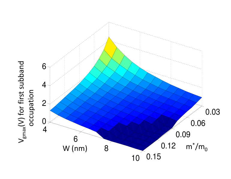
Generally, a qualitative definition, namely is used to identify whether a transistor is in the QCL or not. To give a more quantitative definition taking care of the infinitely long high energy tail of the Fermi-Dirac probability, in the present work, we choose to call a FET to be operating in the UQCL when more than of the carriers populate the first subband. Note that, in the present context of low and strong geometrical confinement in a nanowire, this formal definition automatically meets . In Fig. 2 we plot the maximum allowed as a function of and to keep at least of the carriers in the first subband. Thus, for any operating point in the (, , ) space that lies below the indicated surface is said to be operating in the UQCL. In the CCL regime, the operating point is expected to be much above the surface where large number of subbands contribute. We also define a region called ‘Quasi-QCL’ which essentially represents those points which are just above the indicated surface in Fig. 2. Limited number of subbands contribute to the total carrier density in this regime. In the rest of the paper, we perform a comparative study of two sets of points in the (, , ) space which are chosen carefully such that one of them (nm) is into or very close to the UQCL regime of operation whereas the other (nm) is closer to the CCL regime. Note that, in both the cases, we assume the same bandgap () of eV to compare them under the same terminal bias conditions. This does not allow the difference in bandgap hide the insights that we are looking for. Though this is a theoretical construct, we do see such examples in reality for semiconductors that are relevant to MOSFET channel. For example, both InxGa1-xAs with and Si1-yGey with have similar bandgap of eV, however they show a wide difference in the electron effective masses [20]-[22]. From Fig. 2, it is understandable that for a given , reducing the nanowire cross section or the effective mass of the channel material will push the operating condition deeper into UQCL.
III-B Gate Capacitance
For an undoped nanowire, the total gate capacitance for the structure in Fig. 1 can be expressed as a summation of the contributions from all the subbands as
| (9) |
where
| (10) |
is the total mobile charge contribution from the subband. Using Eq. (5) and writing in terms of Fermi integral, we obtain
| (11) |
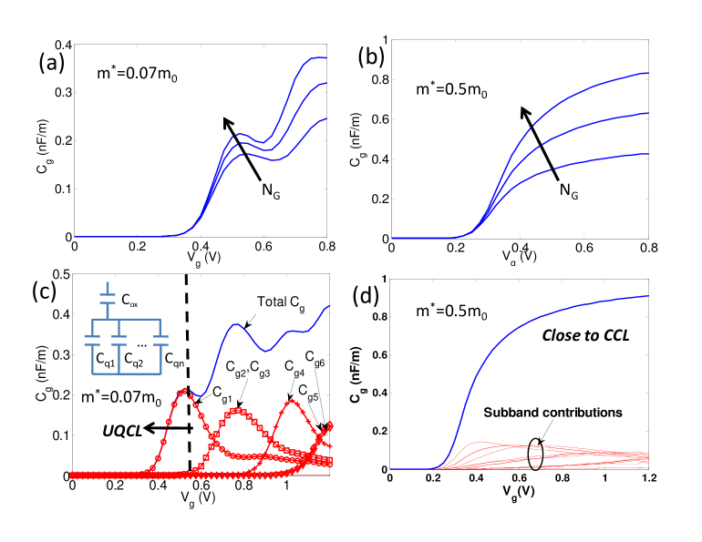
The numerically simulated C-V characteristics are shown in Fig. 3(a) and (b) for multi-gate nanowire in the two different regimes. It is clearly observed that, close to the CCL (Fig. 3(b)), scales almost linearly with the number of gates . However, in the UQCL (Fig. 3(a)), the scaling is much slower with due to the small series quantum capacitance . Consequently, migrating from double-gate to gate-all-around structure is expected to be less effective in the UQCL as compared to CCL regime.
We clearly observe the non-monotonicity of the nanowire C-V characteristics close to UQCL in Fig. 3(a). This is explained in Fig. 3(c) with a ‘parallel-subband-capacitance’ concept using the fact that the total mobile charge is a sum of the contributions from the individual subbands. Elementary electrostatics leads us to an equivalent capacitance model using and individual subband quantum capacitances , as shown in the inset of Fig. 3(c). Unlike 2-D and 3-D structures, in a 1-D nanowire, the DOS of individual subbands falls with energy as (Eq. 5). Into the UQCL, where only one subband contributes, the impact of the DOS is manifested as a drop in after certain . This is arising from the non-monotonic behavior of the function in the Eq. (11). However, as we move away from UQCL, more number of subbands start contributing, and since each of them has its own threshold (Fig. 3(c)), the total gate capacitance shows multiple peaks. Thus, the number of peaks in these highly quantized nanowires is a signature of the number of subbands contributing to the total carrier density. However, as we go closer to CCL, as shown in Fig. 3(d), large number of closely spaced subbands contributing to the total carrier density destroy the humps.
We would like to mention a subtle point here: the physical origin of is different from . When is small, the coupling between the gate and the channel degrades. However, a strongly confined, low channel, resulting in low , provides an excellent gate control allowing the channel to attain almost uniformly the terminal gate voltage with negligible drop across the oxide.
III-C Effect of Interface Traps
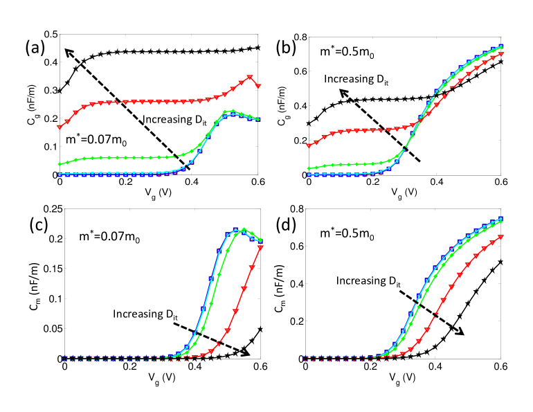
The reduced gate capacitance in the UQCL increases the impact due to the interface traps. The issue is aggravated by the fact that, to date, no high mobility channel MOSFET has been reported with excellent gate insulator interface [10, 23]. Thus, it becomes essential to include the effects of interface traps in the UQCL regime of operation. In this paper, we assume that the trap density is distributed uniformly over the bandgap of the channel material and hence the boundary condition of the normal components of the displacement vectors at the channel-insulator interface is changed to where . is the relative shift in the position of the intrinsic level. In Fig. 4(a) and (b), we plot the capacitance-voltage characteristics in presence of different for UQCL and CCL regime of operation. As expected, for a given , particularly at high , the characteristics are significantly altered, and the effect is more at UQCL compared to CCL. To investigate the effect on mobile charges, we also plot the mobile charge capacitance in Fig. 4(c) and (d) which we define as the rate of change of channel charge due to carriers with respect to gate bias. It clearly shows that with an increase in the , the curves are shifted towards the right along the axis indicating an increase in the threshold voltage.
IV Nanowire FET Characteristics In The UQCL
IV-A Drain Current Saturation
Saturation of the drain current with increase in drain bias is an important requirement for the transistor to be useful for VLSI applications. For example, lack of saturation in the drain current leads to poor transfer characteristics of a CMOS inverter reducing the noise margin of an SRAM cell. In the following, we show that a ballistic FET shows better saturation characteristics in the UQCL regime as compared to the CCL.
Assuming and , Eq. (8) reduces to
| (12) |
where . Clearly, in the saturation region, . Thus, Eq. (12) gives
| (13) |
Integrating,
| (14) |
Now the perturbation to the original Hamiltonian in Eq. (1) due to introduction of the source and drain coupling in Eq. (7) is given by
| (15) |
Using first order perturbation theory, the correction to the energy is obtained as
| (16) |
Hence, assuming source is grounded,
| (17) |
where . We should note that, both and are almost independent of for relatively large in saturation region since the contribution of to top of the source barrier carrier density becomes relatively negligible in Eq. (3). Thus, Eq. (14) reduces to
| (18) |
where . Here, is the only parameter that is dependent on . Thus, we can find the slope of the drain current in saturation region as
| (19) |
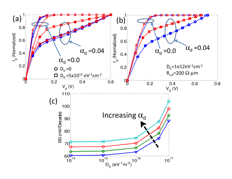
Few conclusions can be drawn from Eq. (19): (1) If drain coupling parameter (the case of a ballistic long channel hypothetical FET), the second term is very small and the first term goes to zero exponentially with increase in , leading to excellent saturation. This argument supports the results obtained from numerical simulations with , as shown in Fig. 5(a). (2) For nonzero , does not completely saturate. However, with stronger quantization, the magnitude of is larger which in turn reduces , hence reducing the magnitude of both the terms in Eq. (19). Consequently, if we operate close to the UQCL, a short channel ballistic FET will show better saturation characteristics as compared to a FET operating close to CCL. Similar conclusion can be drawn from the results of numerical simulations shown in Fig. 5(a) for =0.04 and =0.
The presence of finite screens the gate voltage reducing the magnitude of which in turn degrades the saturation characteristics. In presence of extremely large , as shown in Fig. 5(a), UQCL loses its saturation performance benefit over CCL. In Fig. 5(b), we show the output characteristics of the same devices, but with ==200-m and eV-1cm-2 where it is observed that UQCL operation retains its performance benefit over CCL. This is due to the fact that stronger quantization in the UQCL compared to CCL increases the relative channel resistance, resulting in more immunity from series resistance effect.
From Eq. (18), we can also find the transconductance as
| (20) |
The numerically computed transconductance (not shown) was found to have improved marginally in the UQCL compared to its CCL counterpart.
IV-B Subthreshold Slope
To obtain the subthreshold slope of such a nanowire FET, we find from Eq. (18):
| (21) |
which gives
| (22) |
where . Now, at subthreshold, coupled with the low operation, and which gives . Also, at subthreshold, both and are nearly constant, and let us call them and . Thus we obtain,
| (23) |
Hence, the subthreshold slope is
| (24) |
In the case of infinite channel (==0) with no , putting as , the limit of subthreshold slope reduces to expected (=mV/decade). Note that, both and are relatively insensitive to the region of operation (UQCL or CCL) resulting in similar subthreshold slopes, as shown in Fig. 5(c). The same trend remains even in the presence of moderately large and hence both UQCL and CCL suffer from similar degradation in subthreshold slope in presence of . When and are small, from Eq. 24, we can express in mV/decade as
| (25) |
which explains the almost linear degradation of subthreshold slope with at a given in Fig. 5(c).
IV-C Scaling and Performance
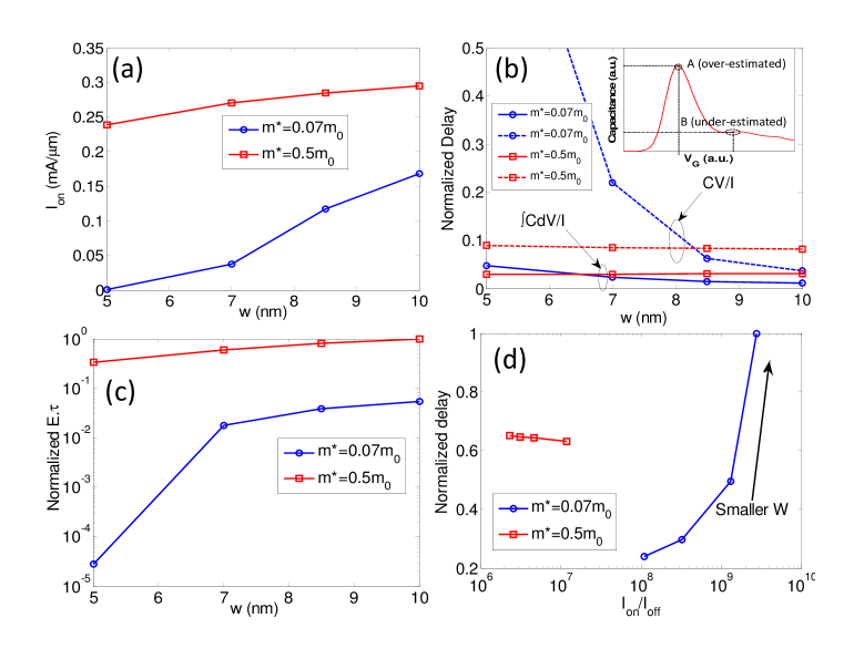
In this section, we will compare the performance of the ballistic nanowire FET between UQCL and CCL. Due to stronger quantization, the ON current, normalized with the perimeter of the nanowire, degrades in the vicinity of UQCL, which is shown in Fig. 6(a). It can also be observed that in this regime, the normalized ON current is more sensitive to the nanowire dimension (), which can be a potential cause to add variability to the device.
Let us now present the relative performance of UQCL and CCL in the light of the performance metrics proposed in [17]. It has been pointed out in [8] that there is no scaling disadvantage in CV/I metric while operating in the UQCL, for both ballistic as well as non-ballistic transport. However, following the discussion of C-V characteristics in sec. III, we wish to point out that CV/I may not be able to reflect the intrinsic gate delay accurately in the UQCL due to the non-monotonic dependence of on . This is explained in the inset of Fig. 6(b) where only one subband contributes to the total mobile charge pushing the transistor deep into UQCL. As shown, CV/I will over estimate the delay at point A whereas at point B, it will under estimate due to wrong computation of the total charge as indicated by the dotted rectangles. We thus take as the delay metric in this work which represents the gate delay more accurately by taking care of the details of the C-V curve.
Fig. 6(b) shows the numerically computed delay as a function of the nanowire dimension from two different metrics. It is found that in the UQCL, CV/I significantly over estimates the delay. However, it becomes closer to the metric as we move out of the UQCL regime (larger ). Note that, in a very narrow nanowire, lower channel material shows higher gate delay due to strong ON current degradation.
Energy-delay product, which has been obtained as , is found to be very impressive at UQCL (Fig. 6(c)) as compared to its CCL counter part. This is because the transistor at UQCL operates at significantly lower switching charge. The normalized delay versus has been plotted in Fig. 6(d) for both UQCL and CCL. It can be clearly seen that at UQCL, the transistor operation can be pushed towards the ideal right-bottom corner of the delay - space. However, in the extremely deep UQCL (smaller in the plot), the delay performance is adversely impacted due to excessive degradation of ON current.
V Scaling And Performance In Presence Of Non-idealities
The fact that a transistor in its UQCL regime of operation switches relatively small amount of mobile charge, it is prone to performance degradation in presence of parasitic capacitances and traps since the fraction of the useful charge (mobile charge that drives the drain current) reduces significantly in the total switching charge. Here we separately discuss the effects of the interface traps, parasitic capacitance and source/drain series resistance, and finally comment on the combined effect of all of them.
Fig. 7(a) shows the effect of on intrinsic delay of the FET, for two different . Increase in increases the threshold voltage reducing the ON current and also increases the unused charge at the dielectric interface, degrading the gate delay. As expected, we observe that the delay in the larger channel is less sensitive to compared to the lower and there is a severe degradation of delay at the narrower dimension for low material. However, at comparatively larger dimension ( 10nm), it is still possible to retain the relative speed advantage of the low case, even with significant . We observe similar trends when we have parasitic capacitance as the only source of non-ideality, as shown in Fig. 7(b). This is again due to the fact that when we are deep into quantum capacitance limit, presence of parasitic capacitance significantly reduces the ratio of mobile charge to total charge that is switched. However, it is interesting to note that the relative degradation of the intrinsic gate delay in the quantum capacitance limit is less compared to the classical capacitance limit in the presence of series source/drain resistance (), which is shown in Fig. 7(c). This arises due to the increased channel resistance in the UQCL due to stronger energy quantization, improving the immunity from parasitic series resistance effect. In fact, deep into the quantum capacitance limit (lower and lower ), presence of series resistance does not at all alter the intrinsic gate delay, as shown in Fig. 7(c). Finally, 7(d) shows the combined effect of all the three non-idealities together which clearly shows a negative impact on the speed advantages that UQCL can have over CCL in the ideal scenario.
In Fig. 8(a), we present the energy-delay product in presence of similar non-ideal conditions showing a significant relative degradation in the UQCL. However, as shown in Fig. 8(b), even in the presence of the non-idealities, UQCL operation manages to offer significantly higher ON to OFF current ratio at comparable gate delays if we choose appropriately. We conclude that the extremely deep UQCL may not be the optimum design for a ballistic nanowire FET in presence of parasitics. At the same time, to retain the OFF performance advantage, better drain current saturation and immunity from series resistance, designing much away from UQCL is also not desirable. The ‘Quasi-QCL’ regime (where few subbands contribute) with low and moderately large , can provide the optimum design to achieve both ON and OFF state performance.
VI Conclusion
To conclude, a ballistic nanowire FET model has been proposed in the work, which is a variation of the ‘Top-of-the-barrier’ model, to analyze the transistor characteristics. The UQCL and CCL regimes have been formally defined in the (, , ) design space based on the subband occupation. The non-monotonic C-V characteristics close to UQCL regime has been explained using a ‘parallel-subband-capacitance’ model. The small quantum capacitance has been found to play a critical role in this regime in presence of interface traps. The saturation characteristics of the drain current are found to improve in the UQCL as compared to CCL regime, both in presence and absence of parasitic resistance and interface traps. It has also been found that the subthreshold slope in UQCL is similar to CCL, even in the presence of interface traps. In the ideal condition, the scaling performance at UQCL regime has been shown to outperform its CCL counterpart. The UQCL operation has been found to be more immune from series resistance effect compared to CCL, whereas the presence of interface traps and parasitic capacitance are shown to diminish the relative performance advantages of the UQCL operation significantly. In presence of the combined effects of all these parasitics, the UQCL operation retains its advantage at comparable gate delay. A careful design in the ‘Quasi-QCL’ regime with low effective mass and moderate nanowire width is required to obtain optimum ON and OFF performance.
Acknowledgement
K.M. and N.B. would like to sincerely acknowledge the support from the Ministry of Communication and Information Technology (MCIT), Govt. of India, and the Department of Science and Technology (DST), Govt. of India.
References
- [1] S. Luryi, “Quantum Capacitance Devices,” Appl. Phys. Lett., Vol. 52, No. 6, pp. 501, 1987.
- [2] D. Vasileska, D. K. Schroder, and D. K. Ferry, “Scaled Silicon MOSFET s: Degradation of the Total Gate Capacitance,” IEEE Trans. Elec. Dev., Vol. 44, No. 4, 1997.
- [3] J. Guo, J. Wang, E. Polizzi, S. Datta and M. Lundstrom, “Electrostatics in Nanowire Transistors,” IEEE Trans. Nanotech., Vol. 2, No. 4, 2003.
- [4] D. L. John, L. C. Castro, and D. L. Pulfrey, “Quantum Capacitance in Nanoscale Device Modeling,” J. Appl. Phys., Vol. 96, No. 9, pp. 5180, 2004.
- [5] D. Vashaee, A. Shakouria, J. Goldberger, T. Kuykendall, P. Pauzauskie, and P. Yang, “Electrostatics of Nanowire Transistors with Triangular Cross Sections,” Appl. Phys. Lett., Vol. 99, pp. 054310, 2006.
- [6] M. V. Fischetti, L. Wangt, B. Yut, C. Sachs, P. M. Asbeckt, Y. Taurt, M. Rodwell, “Simulation of Electron Transport in High-Mobility MOSFETs: Density of States Bottleneck and Source Starvation,” IEDM Tech. Dig., pp. 109-112, 2007.
- [7] P. M. Solomon and S.E. Laux,“The Ballistic FET: Design, Capacitance and Speed Limit,” IEDM Tech. Dig., 2001.
- [8] J. Knoch, W. Riess and J. Appenzeller, “Outperforming the conventional scaling rules in the quantum-capacitance limit,” IEEE Elec. Dev. Lett., Vol. 29, No. 4, pp. 372, 2008.
- [9] S. Ilani, L. A. K. Donev, M. Kindermann and P. L. Mceuen, “Measurement of the Quantum Capacitance of Interacting Electrons in Carbon Nanotubes,” Nature Phys., Vol. 2, pp. 687, 2006.
- [10] S. Roddaro, K. Nilsson, G. Astromskas, L. Samuelson, L. E. Wernersson, O. Karlstr m, and Andreas Wacker, “InAs nanowire metal-oxide-semiconductor capacitors,” Appl. Phys. Lett., Vol. 92, pp. 253509, 2008.
- [11] K. Natori, “Ballistic metal-oxide-semiconductor field effect transistor,” J. Appl. Phys., Vol. 76, No. 8, pp. 4897, 1994.
- [12] A. Rahaman, J. Guo, S. Datta and M. Lundstrom, “Theory of Ballistic Nanotransistors,” IEEE Trans. Elec. Dev., Vol. 50, No. 9, pp. 1853 - 1864, 2003.
- [13] J. Wang and M. Lundstrom, “Ballistic Transport in High Electron Mobility Transistor,” IEEE Trans. Elec. Dev., Vol. 50, No. 7, pp. 1604-1609, 2003.
- [14] A. Rahaman, G. Klimeck and M. Lundstrom, “Novel Channel Materials for Ballistic Nanoscale MOSFETs - Bandstructure Effects,” IEDM Tech. Dig., pp. 615-618, 2005.
- [15] M. A. Khayer and R. Lake, “Performance of n-Type InSb and InAs Nanowire Field-Effect Transistors,” IEEE Trans. Elec. Dev., Vol. 55, No. 11, pp. 2939-2945, 2008.
- [16] M. A. Khayer and R. Lake, “The Quantum and Classical Capacitance Limits of InSb and InAs Nanowire FETs,” IEEE Trans. Elec. Dev., Vol. 56, No. 10, pp. 2215-2223, 2009.
- [17] R. Chau et al, “Benchmarking Nanotechnology for High-Performance and Low-Power Logic Transistor Applications,” IEEE Trans. Nanotech., Vol. 4, No. 2, pp. 153-158, 2005.
- [18] J. G. Fossum, L. Q. Wang, J. W. Yang, S. H. Kim and V. P. Trivedi, “Pragmatic design of nanoscale multi-gate CMOS,” IEDM Tech. Dig., pp. 613-616, 2004.
- [19] M. Luisier, N. Neophytou, N. Kharche, and G. Klimeck, “Full-Band and Atomistic Simulation of Realistic 40 nm InAs HEMT,” IEDM Tech. Dig., 2008.
- [20] K. Majumdar, P. Majhi, N. Bhat and R. Jammy, “HFinFET: A Scalable, High Performance, Low Leakage Hybrid N-Channel FET,” IEEE Trans. Nanotech., Vol. 9, No. 3, pp. 342-344, 2010.
- [21] F. Schaffler, “High Mobility Si and Ge Structures,” Semicond. Sci. Technol., Vol. 12 , pp. 1515-1549, 1997.
- [22] http://www.ioffe.ru/SVA/NSM/Semicond/
- [23] N. Goel et. al., “Addressing The Gate Stack Challenge For High Mobility InxGa1-xAs Channels For NFETs,” IEDM Tech. Dig. 2008.
FIGURE CAPTIONS:
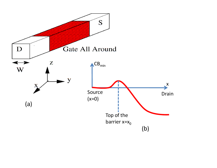
Fig. 1: a): Schematic diagram of a gate-all-around nanowire FET. (b): Locus of the conduction band minimum from source to drain with the top of the barrier height at =.
Fig. 2: UQCL regime of operation in the () space: More than of the carriers populate only the first subband at any operating point below the indicated surface and hence operates in the UQCL, whereas multiple subbands are occupied at points above the surface. The CCL regime, where a large number of subbands contribute, is far above the surface.
Fig. 3: (a): Total gate capacitance for =0.07, =10nm and EOT=1nm (=0.35 in nF/m) shows non-monotonic C-V characteristics. The number gates is 2, 3 and 4. (b): Same as (a) with =0.5. (c): Contribution from individual subbands to the total capacitance causes multi-peak C-V close to UQCL. The inset shows a ‘parallel-subband-capacitance’ model. (d): Large number of subbands contribute to the total capacitance close to CCL resulting a smooth monotonic characteristics.
Fig. 4: Total gate capacitance in presence of interface traps for =10nm with (a): =0.07 and (b): =0.5. The is assumed to be and eV-1cm-2. (c)-(d): The corresponding mobile charge capacitance (rate of change of mobile charge in the channel with ) in the two scenarios.
Fig. 5: (a): Output characteristics of a gate-all-around 10nm X 10nm ballistic nanowire FET with EOT=1nm and =0.6V for =0 and 0.04. The red and blue curves correspond to = 0.07 and 0.5 respectively. The circles and squares correspond to =0 and eV-1cm-2 respectively. (b): The output characteristics in presence of parasitic source and drain resistance of 200-m and eV-1cm-2. The red and blue curves correspond to = 0.07 and 0.5 respectively. (c): Degradation of subthreshold slope with concentration for =0, 0.05, 0.1 and 0.15. The solid and dotted curves (which almost coincide) represent = 0.07 and 0.5 respectively. =0.01 for all the curves.
Fig. 6: (a): ON current as a function of nanowire width . (b): Normalized intrinsic gate delay () computed from two different metrics as a function of for = 0.07 and 0.5. In the inset, The delay predicted by is given by the area of the rectangles shown by the dotted lines, which depends on the operating condition and can either overestimate (at point A) or underestimate (at point B) the actual delay given by . (c): Lower switching charge results in better energy-delay product () at UQCL. (d): Delay versus for different . In all the plots, EOT=1nm, =0.05, =0.01, =0.6V and =0.6V have been assumed.
Fig. 7: (a): Normalized gate delay in presence of (a): only with =0 and =0, (b): only with =0 and =0, (c): only with =0 and =0 and (d) =200-m, =cm-2eV-1 and =0.5nF/m. In all the plots, the blue lines with star and squares represent the reference delay with zero non-ideality for =0.07 and =0.5 respectively. EOT=1nm, =0.05, =0.01, =0.6V and =0.6V have been assumed.
Fig. 8: (a): Energy-delay product and (b) gate delay versus Ion/Ioff plot with =200-m, =cm-2eV-1 and =0.5nF/m. In both the plots, the blue lines with star and squares represent the reference with zero non-ideality for =0.07 and =0.5 respectively. EOT=1nm, =0.05, =0.01, =0.6V and =0.6V have been assumed.