Terahertz radiation-induced conductivity, Kerr and Faraday angles, and spin textures in a two-dimensional electron gas with spin-orbit coupling subjected to a high magnetic field and periodic potential
Abstract
The terahertz radiation-induced conductivity and dielectric polarization tensors as well as the Faraday and Kerr rotation angles and the non-equilibrium spin textures are studied for two-dimensional electron gas with strong spin-orbit coupling subjected to high magnetic field and to tunable periodic potential of a two-dimensional gated superlattice. It is found that both real and imaginary parts of the frequency-dependent induced conductivity approach maximum values with sharp and detectable peaks at frequencies corresponding to the inter-subband transitions between spin-split magnetic subbands. The observed properties of the conductivity tensor frequency dependence are applied for the description of the Kerr and Faraday rotation angles which can be used as another experimental tool for describing the electron gas in periodic structures with significant spin-orbit coupling. The formation of radiation-induced spin textures is predicted having both in-plane and out-of-plane components with space distribution scale comparable to the superlattice cell size which can be observed experimentally.
pacs:
73.21.Cd, 75.70.Tj, 78.67.PtI Introduction
In recent years the spin-dependent properties of heterostructures with Rashba Rashba or Dresselhaus Dresselhaus spin-orbit coupling (SOC) have attracted considerable attention in both fundamental and applied areas of condensed matter physics studying the spin-related phenomena and known as spintronics. Awschalom ; Zutic ; Wu2 The interest in SOC-related effects in semiconductor physics originates from a promising idea of the spin control without an external magnetic field variations as it was proposed, for example, by Datta and Das in their scheme of a spin field-effect transistor.DattaDas Besides the transport measurements and the physics of the spin or charge transfer, the properties of semiconductor heterostructures with SOC caused by an external electromagnetic radiation have also been the topic of an extensive research. The attention given to the radiation-induced properties is natural since, on the one hand, the associated experiments are the usual and reliable tool for determination of various material parameters in condensed matter physics, and, on another hand, a proposal and observation of new externally triggered effects in heterostructures is always of interest for both fundamental problems of condensed matter physics and for the technological applications. Awschalom ; Zutic ; Wu2 These effects are very versatile in their nature and have different measurable parameters, and here we shall focus mainly on the radiation-induced conductivity tensor, on the dielectric matrix, and on the associated Faraday and Kerr rotation angles as well as on the excited non-equilibrium spin textures. The major part of the research in this field considered the metal-based or magnetic semiconductor structures where the conductivity tensor and Kerr effect have been considered, Oppeneer ; Wierman ; Crooker ; Richard ; Antonov ; Sato ; Hamrle ; Kato ; Reichl ; Neudert ; Kim ; Stroppa ; Etz ; Winter although the magnetooptical properties of the molecular semiconductorsFronk and for the systems in the quantum Hall effect regime have also been studied.Volkov Similar effects in non-magnetic semiconductor structures have also been explored, including the Faraday Magarill ; Kato and Kerr Teppe ; Olbrich effects as well as their properties in the presence of a significant SOC in two-dimensional electron gas (2DEG)Zhang and the field-induced non-equilibrium spin density.Bhat ; Tarasenko ; Pletyukhov ; Wu1
Among the various ways of constructing the heterostructure systems with novel properties of quantum states, transport, dynamical and spin-related effects the formation of 2DEG with lateral gated superlattice provides a flexible tool also for the semiconductors with strong SOC. It is well-known that an external electromagnetic field can generate novel effects including spin current injectionSherman1 ; Sherman2 and spin polarization Wu1 ; Wu2 in systems with significant SOC. This has been also demonstrated in SOC superlattices where the properties of quantum states, dynamical and transport properties together with the radiation-induced spin textures have been investigated in 1D superlattices without magnetic field,K4 and the quantum states and quantization of Hall conductance together with magnetooptical properties were studied in 2D superlattices at high magnetic field,DP ; PS respectively. It was found that the gate control together with the external DC electric or electromagnetic excitation can provide new possibilities of controllable manipulations of energy spectrum, charge and spin densities, and the Hall conductivity. Thus, it is of interest to make a step further and to consider the microwave conductance and dielectric matrices together with the excited spin textures for 2DEG with SOC subjected to a high magnetic field and to the tunable periodic potential of a 2D gated superlattice. The properties of energy spectrum and spinor wavefunctions for such system as well as the DC Hall conductance DP and magnetooptical absorption PS have already been studied in detail for both Rashba and Dresselhaus contributions to SOC. The calculations of the magnetooptical conductivity and dielectric tensors and the discussion of the associated Faraday and Kerr effects together with the excited spin textures in such structures are the primary goals of the present paper. We shall focus here on the parameters of the InGaAs/GaAs 2DEG structure with dominating Rashba SOC and on the frequency range of external electromagnetic radiation which may provide the best characteristics of these effects for possible experimental observation and technological applications.
The paper is organized as follows: in Sec.II we briefly describe the Hamiltonian and the quantum states in our system, in Sec.III we calculate and discuss the radiation-induced conductivity and dielectric matrices which are applied in Sec.IV for the calculation of Kerr and Faraday rotation angles, in Sec.V we focus on the induced non-equilibrium spin density forming the spin textures, and the concluding remarks are given in Sec.VI.
II Hamiltonian and quantum states
We consider the 2DEG in the plane in a InGaAs/GaAs heterostructure with the In content of around , where the electron effective mass and -factor are and , respectively, and the SOC is dominated by the Rashba term with a significant amplitude .
The corresponding one-electron Hamiltonian has the following form:DP
| (1) | |||
| (2) |
Here are the momentum operator components, is the electron effective mass, are the Pauli matrices, is the strength of Rashba SO coupling term, is the Landè factor, is the Bohr magneton, and is the unit matrix. We use the Landau gauge in which the vector potential of the static magnetic field has the form , and consider a simple form of the periodic superlattice potential with amplitude and the superlattice period . The structure of the Hamiltonian matrix as well as the matrix elements have been discussed in detail in our previous papers.DP ; PS It was demonstrated that the SOC mixes the states of pure Landau levels and results in a doubling of the number of the magnetic subbands formed under the fixed value of magnetic flux quanta ( and are prime integers) per unit cell. For a given magnetic flux the spectrum of Hamiltonian (2) consists of magnetic subbands on the distance of the order near the corresponding Landau levels, each being split by the Zeeman and by the SOC terms.
As to the structure of the eigenstate of the Hamiltonian (2), one can express them as a set of two-component spinors where each component satisfies the generalized Bloch-Peierls conditions in the magnetic elementary cell which is the initial superlattice cell multiplied by the factor of in direction if the Landau gauge is chosen. Correspondingly, the magnetic Brillouin zone is determined by inequalities , , and a two-component spinor wavefunction has the following form:DP ; PS
| (3) | |||
| (6) | |||
| (9) |
Here, , are the simple harmonic oscillator functions, is the magnetic length, and is the cyclotron frequency, , , and is the sample size in the direction which accounts for the wavefunction norm. The expansion coefficients and in (9) are defined together with the energy eigenvalues during the standard diagonalization procedure for the Schröedinger equation.
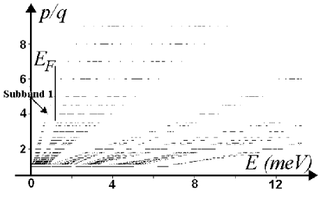
An example of the energy spectrum considered for the following calculations is shown in Fig.1 for the magnetic flux region with corresponding to Tesla and for the superlattice potential amplitude meV. Here the periodic potential amplitude and the SOC energy have the same order, so the inequality takes place, and one can use a two-level approximation where the higher Landau levels do not provide a significant contribution to the quantum states and the associated effects for two lowest Landau levels. Below we set corresponding to the magnetic field T in a superlattice with period nm, and the Fermi level is located in the gap above the lowest subband marked by arrow in Fig.1. One can see that the photon energy for the inter-subband transitions here is of the order of meV corresponding to the frequency which is the terahertz range being of high interest for the current research in magnetooptical properties of semiconductor heterostructures. In a real semiconductor structure with SOC superlattice such position of the Fermi level corresponds to the concentrations of about . Of course, the manifestation of such tiny and fragile miniband structure as on Fig.1 in measurable experimental phenomena requires the preparation of high-purity samples and low temperatures inside experimental setups which, as it is known, is still a conventional condition for monitoring the SOC-related effects in GaAs-based semiconductors where the SOC is relatively weak.
III Microwave conductivity and dielectric tensors
In this Sec. we shall consider the microwave conductivity and dielectric tensors describing the effects of perturbation caused by the external monochromatic and linearly polarized electromagnetic field with vector potential where . Under the dipole approximation the amplitude of the photon wavevector is negligible compared to the electron quasimomentum which leads to the following form of the perturbation Hamiltonian in the presence of the Rashba SOC:
| (10) |
The main distinguishable property of (10) compared to the system without SOC is the presence of second term which is spin-dependent and linear in the Rashba SOC strength. The SOC also introduces the spin-dependent term into the velocity operator which components in the basis of the eigenstates have the following matrix form:
| (11) |
| (12) |
With the known eigenfunctions (9) the matrix elements (11), (12) can be expressed directly via the wavefunction coefficients and as
| (13) | |||
| (14) |
| (15) | |||
| (16) | |||
| (17) | |||
| (18) |
which allows to calculate explicitly the components of the conductivity tensor for the frequency range THz corresponding to the transitions between the magnetic subband 1 below the Fermi level and the subbands above the Fermi level shown in Fig.1. The expression for can be derived from the Kubo formulaKubo and is applied for our calculations in the following form: Oppeneer ; Antonov ; Stroppa ; Kubo ; Callaway
| (19) |
where (per unit volume) at zero temperature the sum is taken over all states with energy below and above the Fermi level, respectively, by applying the Fermi distribution function . The expression (19) is written for the absence of scattering, i.e. for the infinite lifetime of the extended Bloch states.Stroppa It can be verified that this approximation remains qualitatively valid for finite lifetime also as long as the subband broadening for the spectrum shown in Fig.1 does not exceed the intersubband spacing which can be achieved in clean heterostructures at low temperatures where the manifestation of the magnetic subband fine structure is visible.DP It should be mentioned also that the longitudinal part of (19) is real while the off-diagonal part has both real and imaginary parts which is a usual property of the radiation-induced conductivity.
The knowledge of the conductivity tensor (19) allows us to calculate directly the components of the frequency-dependent dielectric tensor via a conventional relation
| (20) |
In Fig.2 we show the frequency dependence of real and imaginary parts of (a) , and (b) , which are the only non-vanishing components for the incident radiation linearly polarized along axis and propagating perpendicular to the 2DEG. The bulk dimension of in corresponds to our understanding of the system as having a finite layer thickness parameter which enters below in the corresponding expressions for the Faraday and Kerr rotation angles which typically include such a characteristic of the system as the traveling distance or thickness. By analyzing Fig.2 one can see that the components of both the conductivity and the dielectric tensors reach their local maximum values at frequencies corresponding to the distance between centers of the magnetic subbands shown in Fig.1. One can see that the induced off-diagonal component of the dielectric tensor at certain frequencies can be quite significant and reach the magnitude of the order of which is a sizable off-diagonal contribution to the static dielectric constant which is about .Goldberg The detailed structure of the conductivity plots in Fig.2(a) near THz where some of the conductivity components change their sign is marked by rectangle and will be discussed below. The practical value of the results shown in Fig.2 is well-known: since the measurements of the radiation-induced conductivity are among the most popular experimental tools for determining the parameters of heterostructures, our calculations provide a useful prediction of experimentally measurable quantities suitable for description of actually used structures with strong SOC.
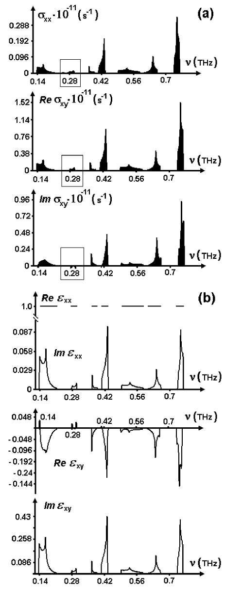
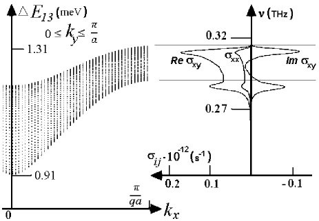
The detailed structure of the photon energy dependence of the conductivity and dielectric tensor components shown in Fig.2 can be clarified to some extent if we consider it together with the energy dispersion relations in those subband pairs which are relevant for the given part of the photon frequency range. In Fig.3 we show the -dependence of the energy difference between the subbands 1 and 3 corresponding to the frequency range on the inset in Fig.2. The whole energy range is covered by running the component over half on the Brillouin zone range , and the component in Fig.3 varies between and (here ) since the subband energy spectrum in the square lattice with Rashba SOC is invariant under the transformations .DP By comparing the energy dispersion on the left side of Fig.3 with the conductivity frequency dependence on the right side plotted on the same energy scale one can connect some specific points of the conductivity plots with the properties of the energy difference dispersion relation. In particular, the points where the imaginary part of component responsible for the direction of Kerr angle changes its sign clearly corresponds to the areas in the plot for the energy difference function for the subbands and , respectively, where the second order derivatives, i.e. the curvature of the function changes its sign. Such connections between the conductivity and the dispersion relations are not uncommon K4 ; DP since the former is determined in (19) via the matrix elements of the velocity operators which, in turn, depend on the shape of the dispersion relation in the particular -th miniband. The example shown in Fig.3 once again demonstrates the importance of the conductivity tensor calculations since its experimental measurement is possible and may provide us with certain information about the topological structure of the energy subbands of such non-trivial system as the 2D superlattice with Rashba SOC in the magnetic field considered here.
IV Faraday and Kerr rotation angles
The knowledge of the radiation-induced conductivity tensor can be applied for determination of (depending on the setup) the Kerr or Faraday rotation angles which are often used for experimental characterization of various heterostructures.Oppeneer ; Wierman ; Crooker ; Richard ; Antonov ; Sato ; Hamrle ; Reichl ; Neudert ; Kim ; Stroppa ; Etz Since the most straightforward manifestation of the Faraday or Kerr rotation is the rotation of the polarization plane on a specific angle, we consider in our manuscript the linearly polarized incident radiation incoming perpendicular to the 2DEG plane with the electric field vector parallel to the axis, . The interaction of external field with the media may generate the -component of the electric field which corresponds to the rotation angle described simply as Volkov . It is clear that although this rotation angle arises due to the application of the external field, its magnitude is not directly related to the strength of the field components due to the expression with a fraction where the common field amplitude is cancelled, and thus can be measurable even for moderated excitation amplitudes. It is known that the rotation angle can be defined as the rotation per unit distance traveled by the incident wave without taking into account a specific thickness of the structure.Magarill In this paper we apply the term ”2DEG”; however, one should keep in mind that it is essentially contained in a triangular InGaAs/GaAs quantum well with finite thickness which value affects the actual rotation angle as the travel distance. In the following calculations we use a typical value nm, and we apply an expression for the Faraday rotation angle derived for a thin film with thickness (here where is the incoming wavelength) deposited on a GaAs substrate with the index of refraction Goldberg which has the following form:Kim ; Volkov ; Magarill
| (21) |
where . The Faraday effect involves the transmission of the incident radiation, and one has the real part of the off-diagonal conductivity present in (21). It is clear that in the limit of a very thin 2DEG layer or in frequency intervals where the longitudinal conductivity drops, the Faraday angle is determined solely by the off-diagonal part of the conductivity tensor,
| (22) |
in accordance with what has been shown earlier.Volkov ; Magarill Then, under the same approximations one can apply also the relation for Kerr angle which reads as Kim
| (23) |
and is determined by the reflection, i.e., imaginary part of the off-diagonal component of the conductivity tensor.
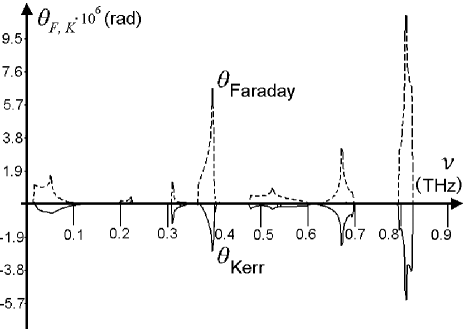
It is clear that here both Faraday and Kerr angles are determined by the conductivity tensor components only, and thus the frequency dependence of discussed above and shown in Fig.2 can be directly applied for the calculation of the frequency dependencies of the Faraday and Kerr angles which are shown in Fig.4. A detailed comparison of Fig.2 and Fig.4 leads to the conclusion that the peaks of the Faraday or Kerr rotation angle correspond mainly to the intervals where at the same frequency the longitudinal conductivity is small and the off-diagonal part is finite, i.e. for the samples in the insulator regime where only the transverse current is induced by the external radiation. The opposite sign of the Kerr angle compared to the Faraday angle which can be observed on the dominating part of the frequency range in Fig.4 can be explained by drawing the attention to the opposite signs in the expressions (21) and (23) reflecting the additional phase rotation during the reflection for the Kerr effect compared to the absorption for the Faraday effect, and the observation that both and have mainly constant signs in the frequency regions when they are both significantly non-zero with relatively small exceptions such as the region in Fig.3 discussed in detail above. It should be noted that the magnitude of both Faraday and Kerr angles shown Fig.4 is rather small compared, for example, with the ones for the interband transitions in ferromagnets or metal-doped semiconductors Kim ; Stroppa ; Winter while being comparable to the Faraday angle for strained GaAs or InGaAs non-magnetic semiconductor structures,Kato , to the Kerr angle in some layered metal structures Etz or organic molecular semiconductors.Fronk Nevertheless, it should be stressed that the frequency dependence of Faraday or Kerr rotation angles provide a quantitative experimental tool for investigation of such fragile and sophisticated spectrum as the miniband structure of a superlattice with SOC in high magnetic field.
V Induced spin textures
In systems with SOC the response to the external electromagnetic radiation can be seen not only in charge but also in spin degrees of freedom. The arising non-equilibrium distributions of local spin density hereafter called the spin texturesK4 are promising for further applications in spintronics and we believe that they can be probed, as any other induced magnetic polarization, by microscopic magnetization detectors Awschalom ; Zutic ; Wu2 as the areas of local magnetization with spatially varying direction, by the Faraday rotation measurements Kato or Kerr microscopy.Neudert Staying in the framework of the linear response theoryKubo one can obtain the excited spin density in the same fashion as the charge conductivity (19), namely,
| (24) | |||
| (25) |
where is the electric field amplitude in the incident wave, and the function does not include the integration over space and thus cannot be referred as a matrix element of the spin operator but instead can be described as the position-dependent interband spin density function reading as
| (26) |
The quantity has the meaning of the local spin density created in the given point of the superlattice by the external electromagnetic radiation with frequency with polarization which is fixed in our problem as , and therefore this index is omitted below. The results for induced spin texture components corresponding to two peaks of the conductivity (Fig.2) or rotation angle (Fig.4) frequency dependencies for THz and THz are shown below in Fig.5 and Fig.6, respectively, in one superlattice cell normalized on the superlattice unit cell area , i.e. the magnetic moment being actually measured by the probe with area can be obtained after multiplying the spin density by a factor . The spin textures are shown in units for the degree of carrier polarization (i.e. in units of Bohr magneton per carrier) for the incident power of which is accessible in modern experiments with nanostructures. It can be seen that all components of the induced spin density are excited on a comparable scale shown in figures (a)-(c), correspondingly which makes these predicted space distributions promising for the experimental observations.
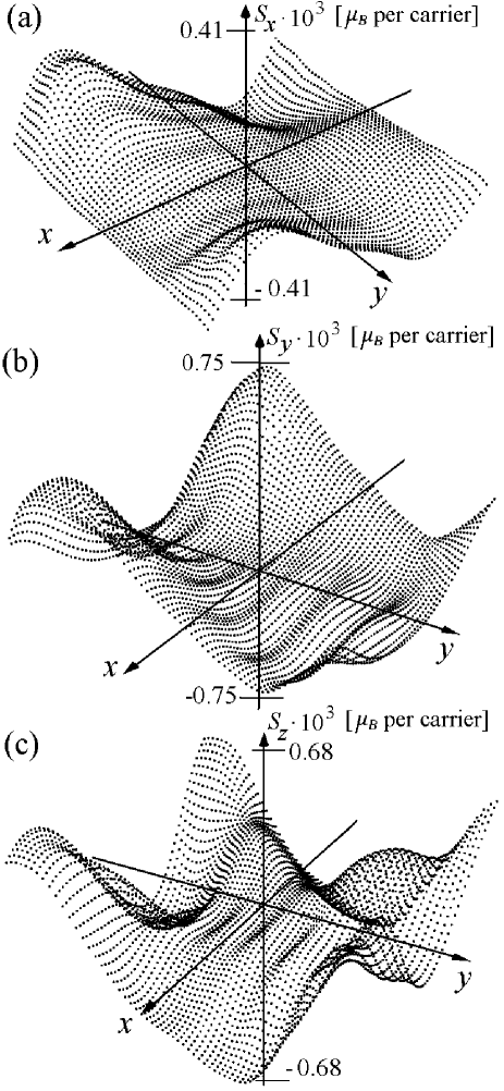
The explanation of the rich spin texture structure can be drawn if we take into account the presence of static magnetic field along direction together with the Rashba SOC in the plane which, in combinations with the linearly polarized radiation along axis may indeed create the excited spin textures with all spin components being non-zero. As to the dominating space scale of the spin texture shape which can be observed in Fig.5,6, one can see that it is comparable with the superlattice size which is the lateral size of the figure being also the scale of the corresponding wavefunctions shape.DP The integration of the spin density components (25) over the superlattice cell indicates that all mean values for spin texture components in Fig.5,6 are very close to zero. This result means that the external radiation which is treated as a perturbation provides no significant gross change in the magnetization over the whole sample but it indeed can alter the local magnetization in different parts of the structure.
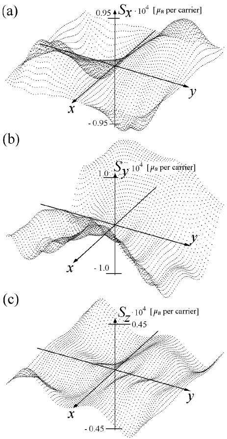
The transitions corresponding to the higher frequency THz with spin textures in Fig.6 occur between the lowest occupied subband 1 in Fig.1 and higher subbands compared to the transitions with textures in Fig.5, i.e. they are located to the right along the energy axis at the line in Fig.1. The calculation of induced spin textures at different excitation frequencies is also important for possible further applications of the observed effects at variable parameters. The results for excitation frequency THz are shown in Fig.6 where again (a) (b) and (c) spin density components, respectively, are shown on separate plots in one square superlattice cell.
If one compares the induced spin textures in Fig.5 and Fig.6 for different excitation frequencies, both common and distinct features can be found. The common features are the comparable space period and global shape of the excited textures for all spin components on both figures. This commonalty is stipulated by the common structure of initial and final quantum states for both examples including the space distribution of charge and spin density. Besides, for any excitation frequency the resulting excited spin textures is formed in principal by all allowed transitions between many states below and above the Fermi level, and thus one may expect certain degree of commonalty between them.
As to the difference between the spin textures at different excitation frequencies in Fig.5 and Fig.6, one can observe the following. First, for the lower frequency THz in Fig.5 all three excited spin components have a higher magnitude. The explanation can be obtained by taking into account the higher position in energy of the final quantum states for the induced textures in Fig.6 which are characterized by more complicated and faster oscillating wavefunctions,DP ; PS which, in turn, reduce the magnitude of the corresponding matrix elements and create the spin density with lower magnitude in Fig.6 compared to Fig.5. The same physical mechanism is responsible for the in general more curved shape of the spin textures in Fig.6 compared to the ones in Fig.5, i.e. the transitions to the quantum states with higher energy leads to the richer space shape of the excited spin textures.
It should be mentioned again that in Eq.(25) the resulting excited spin textures are formed by all allowed transitions and by many states below and above the Fermi level and thus have an integral and pretty universal nature. First of all, this circumstance makes them robust to some extent against the possible corrections to our model, i.e. the finite sample size, the finite temperatures, the scattering on defects and phonons, and the presence of other small terms absent in our Hamiltonian. Then, these spin textures can be viewed as measurable quantities which can be obtained by a probe at a given point and thus can be considered as a promising degree of freedom for further applications such as information processing and storage in spintronics. It is interesting to note that the features of the excited spin density discussed here were also observed in qualitatively the same manifestation and with the same space shape in a different system with 2DEG and SOC subjected to periodic potential of 1D superlattice without the static magnetic field but either under scattering or under radiative (with various polarizations) or DC electric current excitation K4 which allows to consider them as an intrinsic characteristic of low-dimensional systems with strong SOC and non-uniform periodic potential.
VI Conclusions
We have studied the terahertz radiation-induced conductivity and dielectric polarization tensors, the Kerr and Faraday rotation angles, and the excited spin textures for two-dimensional electron gas with strong spin-orbit coupling subjected to high magnetic field and to tunable periodic potential of a two-dimensional gated superlattice. It was found that both real and imaginary parts of the frequency-dependent conductivity approach maximum values with sharp and detectable peaks at frequencies corresponding to the inter-subband transitions between spin-split magnetic subbands. The observed properties of the conductivity tensor frequency dependence were applied for the description of the Kerr and Faraday rotation angles which can be used as another experimental tool for describing the electron gas in periodic structures with significant spin-orbit coupling. The formation of radiation-induced spin textures is predicted having both in-plane and out-of-plane components with space distribution scale comparable to the superlattice cell size which can be promising in further experimental and technological applications.
Acknowledgments
The authors are grateful to V.Ya. Demikhovskii and A.M. Satanin for helpful discussions. The work was supported by the RNP Program of Ministry of Education and Science RF (Grants No. 2.1.1.2686, 2.1.1.3778, 2.2.2.2.4297, 2.1.1.2833), by the RFBR (Grants No. 09-02-01241a, 09-01-00268a), by the USCRDF (Grant No. BP4M01), and by the President of RF Grant for young candidates of science No. MK-1652.2009.2.
References
- (1) E.I. Rashba, Fiz. Tverd. Tela (Leningrad) 2, 1224 (1960) [Sov. Phys. Solid State 2, 1109 (1960)]; Y.A. Bychkov and E.I. Rashba, J. Phys. C 17, 6039 (1984).
- (2) G. Dresselhaus, Phys. Rev. 100, 580 (1955).
- (3) Semiconductor Spintronics and Quantum Computation, edited by D.D. Awschalom, D. Loss, and N. Samarth, Nanoscience and Technology (Springer, Berlin, 2002)
- (4) I. Zǔtić, J. Fabian, and S. Das Sarma, Rev. Mod. Phys. 76, 323 (2004).
- (5) M.W. Wu, J.H. Jiang, M.Q. Weng, Physics Reports 493, 61 (2010).
- (6) S. Datta and B. Das, Appl. Phys. Lett. 56, 665 (1990).
- (7) P.M. Oppeneer, T. Maurer, J. Sticht, and J. Kübler, Phys. Rev. B 45, 10924 (1992).
- (8) K.W. Wierman, J.N. Hilfiker, R.F. Sabiryanov, S.S. Jaswal, R.D. Kirby, and J.A. Woollam, Phys. Rev. B 55, 3093 (1997).
- (9) S.A. Crooker, D.D. Awschalom, J.J. Baumberg, F. Flack, and N. Samarth, Phys. Rev. B 56, 7574 (1997).
- (10) N. Richard, A. Dereux, T. David, E. Bourillot, J.P. Goudonnet, F. Scheurer, E. Beaurepaire, and G. Garreau, Phys. Rev. B 59, 5936 (1999).
- (11) V.N. Antonov, V.P. Antropov, B.N. Harmon, A.N. Yaresko, and A.Ya. Perlov, Phys. Rev. B 59, 14552 (1999).
- (12) K. Sato, A. Kodama, M. Miyamoto, A.V. Petukhov, K. Takanashi, S. Mitani, H. Fujimori, A. Kirilyuk, and T. Rasing, Phys. Rev. B 64, 184427 (2001).
- (13) J. Hamrle, J.Ferré, M. Nývlt, and Š. Višňovský, Phys. Rev. B 66, 224423 (2002); J. Hamrle, J.Ferré, J.P. Jamet, V. Repain, G. Baudot, and S. Rousset, Phys. Rev. B 67, 155411 (2003).
- (14) Y.K. Kato, R.C. Myers, A.C. Gossard, and D.D. Awschalom, Phys. Rev. Lett. 93, 176601 (2004).
- (15) I. Reichl, R. Hammerling, A. Vernes, P. Weinberger, C. Sommers, and L. Szunyogh, Phys. Rev. B 70, 214417 (2004).
- (16) A. Neudert, J. McCord, D. Chumakov, R. Schäfer, and L. Schultz, Phys. Rev. B 71, 134405 (2005).
- (17) M.-H. Kim, G. Acbas, M.-H. Yang, I. Ohkubo, H. Christen, D. Mandrus, M.A. Scarpulla, O.D. Dubon, Z. Schlesinger, P. Khalifah, and J. Cerne, Phys. Rev. B 75, 214416 (2007).
- (18) A. Stroppa, S. Picozzi, A. Continenza, M.Y. Kim, and A.J. Freeman, Phys. Rev. B 77, 035208 (2008).
- (19) C. Etz, A. Vernes, L. Szunyogh, and P. Weinberger, Phys. Rev. B 77, 064420 (2008).
- (20) A. Winter, H. Pascher, M. Hofmayer, H. Krenn, T. Wojtowicz, X. Liu, and J.K. Furdyna, Rev. Adv. Mater. Sci. 20, 92 (2009).
- (21) M. Fronk, B. Bräuer, J. Kortus, O.G. Schmidt, D.R.T. Zahn, and G. Salvan, Phys. Rev. B 79, 235305 (2009).
- (22) V.A. Volkov and S.A. Mikhailov, J. Exp. Theor. Phys. Lett. 41, No.9, p.476 (1985) [Pis’ma v ZhETF 41, No.9, p.389 (1985)].
- (23) L.I. Magarill and V.N. Sozinov, J. Exp. Theor. Phys. Lett. 52, No.11, p.649 (1990) [Pis’ma v ZhETF 52, No.11, p.1230 (1990)].
- (24) F. Teppe, M. Vladimirova, D. Scalbert, M. Nawrocki, and J. Cibert, Solid State Comm. 128, 403 (2003).
- (25) P. Olbrich, J. Allerdings, V.V. Bel’kov, S.A. Tarasenko, D. Schuh, W. Wegscheider, T. Korn, C. Schüller, D. Weiss, and S.D. Ganichev, Phys. Rev. B 79, 245329 (2009).
- (26) F. Zhang, H.Z. Zheng, Y. Li, J. Liu, and G.R. Li, Europhys. Lett. 83, 47006 (2008).
- (27) R.D.R. Bhat, F. Nastos, Ali Najmaie, and J.E. Sipe, Phys. Rev. Lett. 94, 096603 (2005).
- (28) S.A. Tarasenko, Phys. Rev. B 72, 113302 (2005); Phys. Rev. B 73, 115317 (2006).
- (29) M. Pletyukhov and A. Shnirman, Phys. Rev. B 79, 033303 (2009).
- (30) E.Ya. Sherman, A. Najmaie, and J.E. Sipe, Appl. Phys. Lett. 86, 122103 (2005).
- (31) A. Najmaie, E.Ya. Sherman, and J.E. Sipe, Phys. Rev. Lett. 95, 056601 (2005).
- (32) J.H. Jiang, M.W. Wu, and Y. Zhou, Phys. Rev. B 78, 125309 (2008).
- (33) V.Ya. Demikhovskii and D.V. Khomitsky, JETP Letters 83, iss.8, p.340 (2006) [Pis’ma v ZhETF 83, iss.8, p.399 (2006)]; D.V. Khomitsky, Phys. Rev. B 76, 033404 (2007); Phys. Rev. B 77, 113313 (2008); Phys. Rev. B 79, 205401 (2009).
- (34) V.Ya. Demikhovskii and A.A. Perov, Europhys. Lett. 76, 477 (2006); Phys. Rev. B 75, 205307 (2007).
- (35) A.A. Perov and L.V. Solnyshkova, JETP Letters 88, No.9, p.625 (2008) [Pis’ma v ZhETF 88, No.9, p.717 (2008)]; Semiconductors 43, No.2, p.202 (2009) [Fizika i Tekhnika Poluprovodnikov 43, No.2, p.214 (2009)].
- (36) R. Kubo, J. Phys. Soc. Jpn. 12, 570 (1957).
- (37) C.S. Wang and J. Callaway, Phys. Rev. B 9, 4897 (1974).
- (38) Goldberg Yu.A. and N.M. Schmidt Handbook Series on Semiconductor Parameters, vol.2, M. Levinshtein, S. Rumyantsev and M. Shur, ed., World Scientific, London, 1999, pp. 62-88.