Conducting Jahn-Teller Domain Walls in Undoped Manganites.
Abstract
We investigate the electronic properties of multi-domain configurations in models for undoped manganites by means of variational and Monte Carlo techniques. These materials display simultaneous Jahn-Teller distortions and magnetic ordering. We find that a band of electronic states appears associated with Jahn-Teller domain walls, and this band is localized in the direction perpendicular to the walls. The energy and width of this band depends on the conformational properties of the domain walls. At finite temperatures, the conductance along the domain walls, induced by the localized domain wall bands, is orders magnitude larger than in the bulk.
I introduction
In the quest to understand and control the properties of broken symmetry phases, domain walls play a central role. Among the many materials with ground state broken symmetries, strongly correlated transition metal oxides, and manganites among them, are particularly interesting. In these compounds several degrees of freedom are simultaneously important, and different broken symmetry phases with similar characteristic energy scales either compete, as in phase separated materials,Dagotto (2005) or coexist, as it occurs in multiferroics. Cheong and Mostovoy (2007); Eerenstein et al. (2006) Research on magnetic domain walls in general has been particularly intense, and it has proven to be extremely important to explain the static and dynamic properties of magnetic materials. Early work Kittel (1949); Lifshitz et al. (1984) led to the development of a variety of important concepts to understand domain walls. Technological applications, and the need to control and understand the important details of domain walls, stimulated considerable and wide research on this topic,Tatara and Kohno (2004); Kläui et al. (2005); Tatara and Fukuyama (1997); Marrows (2005) unveiling a variety of interesting aspects of these walls. In particular, the magnetic domain walls of manganites, the materials with the colossal magnetoresistance, have also attracted much attention. Already in Ref. Schiffer et al., 1995, the large magnetoresistance was attributed to domain wall scattering, an hypothesis that led to both experimental and theoretical work on the subject of resistance of domain walls. Li et al. (2001); Levy and Zhang (1997); Mathur et al. (1999); Suzuki et al. (2000); Golosov (2003); Yamanaka and Nagaosa (1997); Becker et al. (2002); Singh-Bhalla et al. (2009) Recently, it was shown that magnetic domain walls in a ferromagnetic metallic material could be insulating.Arnal et al. (2007)
Similarly, domain walls and gradients of the order parameter play a crucial role in our understanding of other collective phenomena, such as superconductivity, Ginzburg and Landau (1950) and ferroelectrity.Streiffer et al. (2002); Aguado-Puente and Junquera (2008) Early theoretical work showed that physical properties absent in bulk materials can arise in domain walls,Přívratská and Janovec (1997) and the conductivity of ferroelastic domain walls has been showed to be different from the conductivity in the bulk.Aird and Salje (1998); Bartels et al. (2003) Another very interesting field is the study of properties of domain walls in multiferroics, or magnetoelectric materials. Different orderings can change across domain walls in these materials, and indeed it has been observed than often the change in one order parameter is correlated with modifications in another.Fiebig et al. (2002) The interplay between order parameters can affect the physical properties of domain walls. In the antiferromagnetic and ferroelectric phases of hexagonal HoMnO3,Lottermoser and Fiebig (2004) there is a transition between two symmetry nonequivalent antiferromagnetic phases. Wide domain walls where the spins rotate smoothly appear close to this transition, producing a pronounced magnetoelectric behavior. Interestingly, this behavior is not observed associated with the abrupt domain walls where magnetization reversal is coupled to a change in the ferroelectric order parameter. In helicoidal magnetic manganites, with a perovskite crystal structure, the study of the dielectric dispersion and its behavior varying the temperatureKagawa et al. (2009) allowed to identify the motion of domain walls as the origin of the substantial enhancement of the dielectric constant in materials like DyMnO3 and TbMnO3.
Of particular motivational interest for the work described here is Ref. Seidel et al., 2009, where manipulation and characterization of domain walls in ferroelectric and antiferromagnetic BiFeO3 was demonstrated. The authors of that effort could create ferroelectric domain walls and showed that domain walls with particular orientations exhibited larger conductance than others, within an otherwise good insulating material. Contrary to previous work, the authors focused on electronic transport in the direction parallel to the domain walls, instead of transport across them as in other efforts in manganites.Li et al. (2001); Levy and Zhang (1997); Mathur et al. (1999); Suzuki et al. (2000); Golosov (2003); Yamanaka and Nagaosa (1997); Becker et al. (2002); Singh-Bhalla et al. (2009) A very recent work studied domain walls in a non-perovskite oxide.Choi et al. (2010) Domain walls in hexagonal YMnO3 have been shown to be more insulating than in the bulk, an effect actually opposite to the BiFeO3 case. Here, motivated by those previous efforts, we study the electronic properties of domain walls in undoped perovskite manganites. These materials are not only antiferromagnetic insulators, but also have a phase transition above room temperature, where an ordered pattern of distorted MnO6 octahedra sets in. We show that at finite temperature (), structural domain walls display a conductance orders of magnitude larger that the conductance observed in bulk materials.
In particular, we concentrate on the insulating, Jahn Teller (JT) ordered phase of undoped manganites with an A-type spin antiferromagnetic order.Rodríguez-Carvajal et al. (1998); Hotta et al. (2003) Our standard variational and Monte Carlo calculations, using well-tested and reliable models, predict that: (i) domain wall electronic states exist, and are localized in the direction perpendicular to the domain wall. They are analogous to surface states and appear associated with the presence of an structural domain wall. (ii) These states form narrow bands within the energy gap of the bulk material. The periodicity of the structural distortions determine the position and width of theses bands. (iii) At low temperature there is a gap between the domain wall bands, and as increases, conformational changes in the domain wall make the localized bands wider, and induce some spectral weight at the Fermi energy, leading to a finite conductance in the direction parallel to the domain walls.
II Model and Techniques
II.1 Model Hamiltonian
The Hamiltonian used here is given by:
| (1) |
is the well-known two-orbital double exchange model Hamiltonian. This model describes the kinetic energy of the electrons and their interaction with the magnetic background of the core spins.Dagotto (2002) More precisely, it is given by
| (2) |
Here creates an electron at the Mn site , in the orbital ( with and ). The factor affecting the hopping amplitudes in the limit of an infinite Hund’s coupling depends on the Mn core spins orientation given by the angles and via the double-exchange mechanism . The actual hopping amplitudes take into account the different overlaps between the orbitals along the directions u=,: Slater and Koster (1954) === and ==-=. is taken as the energy unit throughout this work, and its value depends on material details. Comparison between theoretical calculations and experiments suggests that its value is of the order of half an electron volt.Salafranca et al. (2009)
The phononic portion of the Hamiltonian reads:
| (3) |
where is the density operator at site , and and are the corresponding Pauli matrices in the eg subspace, that express the coupling of the lattice distortions, , to the electrons. In particular, is the breathing mode of the MnO6 octahedra around the -th manganese ion, and , are the Jahn Teller modes. Dagotto (2002) = 2 is the stiffness of the breathing mode that effectively takes into account suppressed charge fluctuations due to electron-electron interactions.Hotta et al. (1999)
II.2 Calculation Method
Undoped manganites, such as LaMnO3, crystallize in an orthorhombic structure, with two nonequivalent manganese positions. Hamiltonian (1) has cubic symmetry, but in order to better compare with experiments we maintain the axis and notation corresponding to the orthorhombic unit cell, in particular we call axis the direction perpendicular to the domain walls (see Fig 1). We focus on the antiferromagnetic -type phase,Wollan and Koehler (1955) experimentally found for manganite and other trivalent cations of similar size.Rodríguez-Carvajal et al. (1998) In this A-phase there are ferromagnetic planes coupled antiferromagnetically in the -axis direction. Double exchange effectively decouples electrons in the atomic planes, and 2D systems provide a good description of the physics of these materials. In real compounds, certainly a coupling exists along the axis that prevents 2D fluctuations to dominate the magnetic and electronic properties of these compounds.
The Hamiltonian (1) depends on the octahedra and core spin configurations, and . These have been approximated as classical degrees of freedom, as in most of the theoretical literature on manganites, and they determine the electronic properties of the system. At finite , Monte Carlo simulations allow us to obtain the relevant equilibrium configurations and calculate thermal averages. and are used as the Monte Carlo variables and the resulting quadratic Hamiltonian for each configuration is exactly diagonalized using standard numerical routines.Anderson et al. (1999) Further details about the Monte Carlo method and its application to manganites can be found in Refs. Dagotto, 2002 and Salafranca and Vergés, 2006.
At low enough , only one classical configuration becomes relevant, and it can be determined by a suitable minimization algorithm. The results for =0 presented here have been obtained with the Broyden method. Press et al. (1992) Although it still involves the diagonalizing of the fermionic sector for each step, this minimization process is faster than the standard Monte Carlo method and it can be applied to calculate results on larger clusters. Comparison between results obtained with the two methods shows that size effects are small. This calculation method has been successfully applied to study uniform phases in manganites.Şen et al. (2004); Hotta et al. (2003); Salafranca et al. (2009) Here, with the appropriate boundary conditions discussed below, we study the properties of structural domain walls in undoped Manganites.
The ground state configuration for Hamiltonian (1) with one electron per site is a spin ferromagnetic plane with an ordered pattern of distortions characterized by a (, ) wave vector in the 2D cubic notation. Hotta et al. (2003); Salafranca and Brey (2006) These orderings correspond in 3D to the experimentally observed A-type antiferromagnetic phase, and the (, , 0) JT ordered phase.Rodríguez-Carvajal et al. (1998) In the orthorhombic notation, the two octahedra around the two Mn ions in the unit cell have opposite distortions, one is elongated along the axis, and the other along the axis. The two possible ground state configurations intrinsic of a staggered order parameter (one reachable from the other by merely a global shift in one lattice spacing in any axes direction) are obtained by repeating the two possible units in the and directions. We label the order parameter, whose value is the magnitude of the distortions and its sign distinguishes between the two possible configurations.
Monte Carlo or optimization calculations at low temperatures with standard periodic boundary conditions converge to one of the two possible ground state configurations. In order to study the domain walls that we wish to focus on in this effort different boundary conditions have to be imposed. In a cluster, we fixed sites with coordinate =1 and = to the bulk equilibrium values corresponding to 0, while sites at the center layer = are constrained to have distortions with the same magnitude but corresponding to the other configuration 0. This way, two JT domain walls do appear in the system, and periodic boundary conditions can still be used for the fermionic sector.
The high computational cost of the repeating diagonalizing step of the Monte Carlo algorithm limits the sizes of the simulation cells. The largest cell used in this work is =4, =20, which contains 160 Mn ions (there are two Mns in the orthorhombic unit cell). Thermalization is achieved by 2,000 Monte Carlo steps (as defined in Ref. Salafranca and Vergés, 2006) and measurement averages of 3,000 Monte Carlo configurations are used, taken every three steps to reduce self-correlations. This computational effort corresponds to roughly two days of running in a typical workstation for a 416 system and five days for a 420 system, for each fixed set of parameters in the problem.
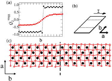
The conductance is calculated within the Landauer formalism, as explained in Ref. Vergés, 1999. To minimize size effects, we calculate the Green function of the system attached to leads that are identical copies of itself. Leads are enlarged by adding more copies of the system until the Green function converges, providing an efficient method to calculate the intrinsic conductance.Salafranca and Vergés (2006) As illustrated in Fig. 1 the conductance of domain walls refers to conductance evaluated in the direction parallel to the domain walls.
III results
Before addressing the results regarding electronic transport, let us discuss the nature of the Jahn Teller domain walls. Figure 1(a) presents the variation of the order parameter as a function of distance across the domain wall. In magnetic domain walls, it is well knownKittel (1949) that the width varies as , where is the magnetic anisotropy and is the spin-stiffness. In the case of an isolated Jahn Teller center, the energy depends on (+) and the anisotropy is zero. The cooperative nature of Jahn Teller effect in manganites and the competition with the kinetic energy double-exchange term (even in the insulating state) gives rise to an effective anisotropy that depends on the value of . These same effects stabilize the order in the plane.Popovic and Satpathy (2000) Therefore, / controls the thickness of the domain wall. Figure 1 (a) shows how an abrupt domain wall is the minimum energy configuration for =1.25, but for =1, the domain wall expands over several unit cells. The first value provides a more accurate description of the real materials, as it can be deduced by the magnitude of the electronic gap discussed later. A real-space view of the octahedra distortions in the plane for the =1.25 case is presented in Fig. 1(c).
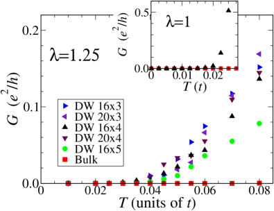
The conductance vs. plots contained in Fig. 2 constitute the main results of this manuscript. The conductance, , refers to the conductance in the direction parallel to the domain wall, as shown in Fig. 1(b), and it is provided as a function of . These results have been obtained by means of Monte Carlo simulations with different system sizes, as indicated in Fig. 2. is essentially zero (within our numerical precision) for bulk configurations, when no domain walls are present, for all the s considered in Fig. 2. However, when domain walls are present in the system, the conductance shows a clear upturn when increasing the temperature. For =1, where the domain wall is fairly wide, this upturn takes place at 0.02, while a larger 0.05 is needed to induce a significant value for in the =1.25 case. There are some size effects in the results, but the increase with temperature of the conductance along domain walls, as compared to its negligible bulk value, is clearly present for all system sizes within our computational capabilities.
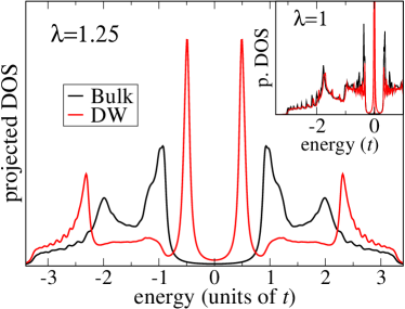
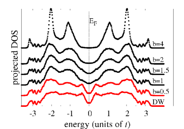
Figure 3 shows the density of states (DOS) projected over different sites at zero . It has been obtained by providing to the eigenenergies arising from the exact diagonalization procedure a small lorentzian width (0.01 ). For the bulk case (no domain walls) the DOS has a large gap due to Jahn Teller effects. This gap scales with : it is roughly 2 for =1.25 and half that value for =1. Considering that is in the range 0.5-1 eV, =1.25 is more consistent with the experimental estimations of the gap (1.6 eV in Ref. Murakami et al., 2006 and 2.5 eV in Ref. Inami et al., 2003).
When the density of states is projected over sites further than 4 unit cells from the domain wall, we recover essentially the bulk density of states. However, a projection over Mn sites close to the domain wall is more interesting. Figure 3 shows that the DOS the closest to the domain wall has some features that do not appear in the bulk region. Two narrow peaks appear at energies located within the bulk energy gap. These two peaks are separated in energy creating a new, smaller, gap that depends strongly on . It is for =1 and increases to for =1.25. The integrated weight of these peaks decays exponentially in the direction, perpendicular to the domain wall, so these states are localized at the domain walls. A least-squares fitting shows that the decay length is of the order of the nearest neighbors distance. The fermionic wave functions coming out of the simulations, via the exact diagonalization procedure, have a well defined momentum in the direction. Therefore, we can state that the new peaks correspond to a band localized in the direction and with a small dispersion () parallel to the domain wall. Note that the artificial broadening 0.01 is not sufficient to understand the width of the in-gap peaks; in fact, the actual dispersion in the direction produces their intrinsic width.
These bands are obvious candidates to explain the conductance results in Fig. 2. Although the energy gap due to the splitting of the localized band is rather small for =1, it is too large to explain the nonzero conductance at =0.05 observed for the more realistic case =1.25. As the electronic states associated with the domain wall disperse in the direction, some splitting due to the periodic Jahn Teller distortions in that direction can be expected. This explains why the splitting decreases with . Note that the conductance calculation has enough precision to determine that the small gap in the =1 case, difficult to appreciate in Fig. 3, still suppresses transport at the lowest temperatures.
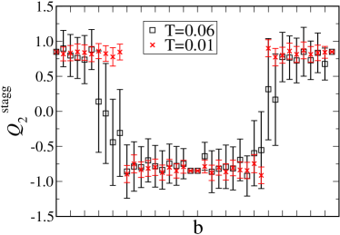
In order to understand the onset of electronic transport with temperature, we examine the structure of the domain walls as increases (Fig. 4), for =1.25. We have observed that the order parameter changes much more abruptly at =0.01 as compared to =0.06. The points in Fig. 4 correspond to average values over 1,500 Monte Carlo steps, with the error bars showing the standard effect of thermal fluctuations. The domain wall is clearly wider for =0.06, with a width that effectively corresponds to a smaller if the calculation were done at very low (as discussed below). Entropy reduces the effective anisotropy (or lowers the order parameter stiffness). A visual inspection of Monte Carlo snapshots, namely equilibrated configurations of classical variables, shows that the widening of the domain wall is due to changes in the intrinsic width, and the contribution from thermal vibrations of the center of the wall is small.
The widening of the domain wall induces changes in the density of states. In Fig. 5 we show the DOS projected on sites at different distances from the domain wall, thermally averaged at =0.06. Particle-hole symmetry was assumed, and the spectrum symmetrized with respect to in order to reduce the noise (Monte Carlo calculations are more noisy than optimization results due to thermal and finite size effects). However, it can be clearly observed how the band associated with the domain wall is now wider in energy, and has some spectral weight at the Fermi energy, that is responsible for the finite conductance. Notice that this band is still localized in the direction and by moving 4 sites away from the domain wall, the bulk density of states is recovered.
An intuitive way to understand the results presented above is to consider that the coupling is now effectively smaller near the domain wall. But note that temperature must also be incorporated. At =0, the domain wall is abrupt for the realistic coupling =1.25, and therefore this coupling produces distortions at the domain wall as large as in the rest of the system. The bands appear associated with the domain wall due to the change in periodicity. For smaller ’s, domain walls are smoother. Wider domain walls have a smaller gap, relative to the bulk gap. For =1.25, the gap between the domain walls gaps is half the bulk value, while is an order of magnitude smaller than the bulk gap for =1. Thus, must also be included to justify the effective reduction of the value of the electron lattice coupling. From the structural point of view, this effect results in a smaller anisotropy and an increase in the domain wall width. As regarding the electronic structure, it reduces the gap between the localized bands, eventually closing it.
IV Conclusions
Stimulated by the recent experimental characterization and manipulation of structural domain walls in a perovskite transition metal oxide,Seidel et al. (2009) we have undertaken the theoretical study of domain walls in undoped manganites. These materials display an ordered phase with an alternating pattern of distorted MnO6 octahedra, and mobile electrons are known to couple strongly to these distortions. The equilibrium configurations and electronic properties of structural domain walls have been examined, and they remarkably differ form the properties of the bulk. Since it is an important characteristic for applications and a property directly measurable by experiments, here special attention has been paid to the electronic conductance of the system.
Electronic transport along structural domain walls is dominated by two narrow electronic bands associated with them. These domain walls electronic states have energies within the bulk energy gap region. At low ’s, domain walls are abrupt, and the narrow bands are separated in energy. The energy gap between them, although smaller than the bulk energy gap, is still large enough to make the conductance negligible at low . However, for ’s of the order of room temperature, thermal fluctuations favor wider domain walls. This makes the dispersion of the domain walls electronic states larger, reducing the energy gap, and inducing some spectral weight at the Fermi energy. Correspondingly, conductance along domain walls is several orders of magnitude larger for the temperature range studied than in the bulk, while it is still zero within our numerical precision for the bulk phase. Our results pose the question of whether the conductance enhancement by domain walls electronic states induced by changes in the periodicity of the system might be a more general phenomenon, and suggest the possibility that they might play a role in recent experiments showing conducting domain walls in a multiferroic perovskite oxide.Seidel et al. (2009) These issues certainly deserve further theoretical and experimental studies.
Acknowledgements.
The authors acknowledge useful conversations with Jan Seidel. This work was supported by the NSF grant DMR-0706020 and the Division of Materials Science and Engineering, Office of Basice Energy Sciences, U.S. Department of Energy. R.Y. acknowledges support from NSF Grant No. DMR-0706625, the Robert A. Welch Foundation Grant No. C-1411, and the W. M. Keck Foundation.References
- Dagotto (2005) E. Dagotto, Science 309, 257 (2005).
- Cheong and Mostovoy (2007) S. Cheong and M. Mostovoy, Nature Materials 6, 13 (2007).
- Eerenstein et al. (2006) W. Eerenstein, N. Mathur, and J. Scott, Nature 442, 759 (2006).
- Kittel (1949) C. Kittel, Rev. Mod. Phys. 21, 541 (1949).
- Lifshitz et al. (1984) E. Lifshitz, L. Landau, and L. Pitaevskii, Electrodynamics of continuous media (Pergamon Press, 1984).
- Marrows (2005) C. Marrows, Adv. Phys. 54, 585 (2005).
- Tatara and Kohno (2004) G. Tatara and H. Kohno, Phys. Rev. Lett. 92, 086601 (2004).
- Kläui et al. (2005) M. Kläui, P.-O. Jubert, R. Allenspach, A. Bischof, J. A. C. Bland, G. Faini, U. Rüdiger, C. A. F. Vaz, L. Vila, and C. Vouille, Phys. Rev. Lett. 95, 026601 (2005).
- Tatara and Fukuyama (1997) G. Tatara and H. Fukuyama, Phys. Rev. Lett. 78, 3773 (1997).
- Schiffer et al. (1995) P. Schiffer, A. P. Ramirez, W. Bao, and S.-W. Cheong, Phys. Rev. Lett. 75, 3336 (1995).
- Golosov (2003) D. I. Golosov, Phys. Rev. B 67, 064404 (2003).
- Li et al. (2001) Q. Li, Y. Hu, and H. Wang, Journal of Applied Physics 89, 6952 (2001).
- Levy and Zhang (1997) P. M. Levy and S. Zhang, Phys. Rev. Lett. 79, 5110 (1997).
- Mathur et al. (1999) N. Mathur, P. Littlewood, N. Todd, S. Isaac, B. Teo, D. Kang, E. Tarte, Z. Barber, J. Evetts, and M. Blamire, Journal of Applied Physics 86, 6287 (1999).
- Suzuki et al. (2000) Y. Suzuki, Y. Wu, J. Yu, U. Ruediger, A. Kent, T. Nath, and C. Eom, Journal of Applied Physics 87, 6746 (2000).
- Yamanaka and Nagaosa (1997) M. Yamanaka and N. Nagaosa, Physica B: Condensed Matter 237, 28 (1997).
- Becker et al. (2002) T. Becker, C. Streng, Y. Luo, V. Moshnyaga, B. Damaschke, N. Shannon, and K. Samwer, Phys. Rev. Lett. 89, 237203 (2002).
- Singh-Bhalla et al. (2009) G. Singh-Bhalla, S. Selcuk, T. Dhakal, A. Biswas, and A. F. Hebard, Phys. Rev. Lett. 102, 077205 (2009).
- Arnal et al. (2007) T. Arnal, A. V. Khvalkovskii, M. Bibes, B. Mercey, P. Lecoeur, and A.-M. Haghiri-Gosnet, Phys. Rev. B 75, 220409(R) (2007).
- Ginzburg and Landau (1950) V. L. Ginzburg and L. D. Landau, h. Eksp. Teor. Fiz. 20, 1064 (1950).
- Streiffer et al. (2002) S. K. Streiffer, J. A. Eastman, D. D. Fong, C. Thompson, A. Munkholm, M. V. Ramana Murty, O. Auciello, G. R. Bai, and G. B. Stephenson, Phys. Rev. Lett. 89, 067601 (2002).
- Aguado-Puente and Junquera (2008) P. Aguado-Puente and J. Junquera, Phys. Rev. Lett. 100, 177601 (2008).
- Přívratská and Janovec (1997) J. Přívratská and V. Janovec, Ferroelectrics 204, 321 (1997).
- Aird and Salje (1998) A. Aird and E. K. H. Salje, Journal of Physics: Condensed Matter 10, L377 (1998).
- Bartels et al. (2003) M. Bartels, V. Hagen, M. Burianek, M. Getzlaff, U. Bismayer, and R. Wiesendanger, Journal of Physics: Condensed Matter 15, 957 (2003).
- Fiebig et al. (2002) M. Fiebig, T. Lottermoser, D. Frqöhlich, A. Goltsev, and R. Pisarev, Nature 419, 818 (2002).
- Lottermoser and Fiebig (2004) T. Lottermoser and M. Fiebig, Phys. Rev. B 70, 220407(R) (2004).
- Kagawa et al. (2009) F. Kagawa, M. Mochizuki, Y. Onose, H. Murakawa, Y. Kaneko, N. Furukawa, and Y. Tokura, Phys. Rev. Lett. 102, 057604 (2009).
- Seidel et al. (2009) J. Seidel, L. Martin, Q. He, Q. Zhan, Y. Chu, A. Rother, M. Hawkridge, P. Maksymovych, P. Yu, M. Gajek, et al., Nature Materials 8, 229 (2009).
- Choi et al. (2010) T. Choi, Y. Horibe, H. Yi, Y. Choi, W. Wu, and S. Cheong, Nature Materials 9, 253 (2010).
- Hotta et al. (2003) T. Hotta, M. Moraghebi, A. Feiguin, A. Moreo, S. Yunoki, and E. Dagotto, Phys. Rev. Lett. 90, 247203 (2003).
- Rodríguez-Carvajal et al. (1998) J. Rodríguez-Carvajal, M. Hennion, F. Moussa, A. H. Moudden, L. Pinsard, and A. Revcolevschi, Phys. Rev. B 57, R3189 (1998).
- Dagotto (2002) E. Dagotto, Nanoscale Phase Separation and Colossal Magnetoresistance (Springer-Verlag, Berlin, 2002).
- Slater and Koster (1954) J. C. Slater and G. F. Koster, Phys. Rev. 94, 1498 (1954).
- Salafranca et al. (2009) J. Salafranca, G. Alvarez, and E. Dagotto, Phys. Rev. B 80, 155133 (2009).
- Hotta et al. (1999) T. Hotta, S. Yunoki, M. Mayr, and E. Dagotto, Phys. Rev. B 60, R15009 (1999).
- Wollan and Koehler (1955) E. Wollan and W. Koehler, Phys. Rev. 100, 545 (1955).
- Anderson et al. (1999) E. Anderson, Z. Bai, C. Bischof, S. Blackford, J. Demmel, J. Dongarra, J. Du Croz, A. Greenbaum, S. Hammarling, A. McKenney, et al., LAPACK Users’ Guide (Society for Industrial and Applied Mathematics, Philadelphia, PA, 1999), 3rd ed.
- Salafranca and Vergés (2006) J. Salafranca and J. A. Vergés, Phys. Rev. B 74, 184428 (2006).
- Press et al. (1992) W. H. Press, S. A. Teukolsky, W. T. Vetterling, and B. P. Flannery, Numerical recipes in FORTRAN. The art of scientific computing (1992).
- Şen et al. (2004) C. Şen, G. Alvarez, and E. Dagotto, Phys. Rev. B 70, 064428 (2004).
- Salafranca and Brey (2006) J. Salafranca and L. Brey, Phys. Rev. B 73, 024422 (2006).
- Vergés (1999) J. Vergés, Comput. Phys. Commun. 118, 71 (1999).
- Popovic and Satpathy (2000) Z. Popovic and S. Satpathy, Phys. Rev. Lett. 84, 1603 (2000).
- Murakami et al. (2006) K. Murakami, T. Yamauchi, A. Nakamura, Y. Moritomo, H. Tanaka, and T. Kawai, Phys. Rev. B 73, 180403(R) (2006).
- Inami et al. (2003) T. Inami, T. Fukuda, J. Mizuki, S. Ishihara, H. Kondo, H. Nakao, T. Matsumura, K. Hirota, Y. Murakami, S. Maekawa, et al., Phys. Rev. B 67, 045108 (2003).