Single shot emittance measurement using Optical Transition Radiation

Nicolas Delerue, Riccardo Bartolini and Cyrille Thomas
( November 2008 )

We describe a method that uses Optical Transition Radiation (OTR) screens to measure in a single shot the emittance of an electron beam with an energy greater than 100 MeV. Our setup consists of 4 OTR screens located near a beam waist. A fit of the 4 profiles allows the reconstruction of the Twiss parameters and hence a calculation of the beam emittance. This layout has been simulated using Mathematica to study its sensitivity to errors and using Geant4 to include effects due to the scattering of the electrons in the screens.
Some assumptions made in this document are conservative to allow for unexpected experimental issues.

1 Emittance measurement using several screens

1.1 Proposed experiments

The measurement of a beam emittance by using several screens one after the other in a linac is a well know technique. We propose to adapt this technique to single shot emittance measurements by using the screens simultaneously. This requires the use of very thin screens. In our simulations we have used 3 screens located 0.5m apart from each other followed by a 4th screen located 1m beyond the 3rd screen.

Refer to caption
Figure 1: Proposed layout

1.2 Beam propagation in a drift space

In a drift space the beam (σ𝜎\sigma) size evolves as [1]:

σ(s)=ϵ(β02α0s+γ0s2)𝜎𝑠italic-ϵsubscript𝛽02subscript𝛼0𝑠subscript𝛾0superscript𝑠2\sigma(s)=\sqrt{\epsilon(\beta_{0}-2\alpha_{0}s+\gamma_{0}s^{2})} (1)

where s𝑠s is the position in the drift space, α0subscript𝛼0\alpha_{0}, β0subscript𝛽0\beta_{0} and γ0subscript𝛾0\gamma_{0} are the Twiss parameters at s=0𝑠0s=0 and ϵitalic-ϵ\epsilon is the beam emittance.

When s=0𝑠0s=0 is a symmetry point (waist), this can be rewritten as

σ(s)=ϵβ0+ϵβ0s2𝜎𝑠italic-ϵsubscript𝛽0italic-ϵsubscript𝛽0superscript𝑠2\sigma(s)=\sqrt{\epsilon\beta_{0}+\frac{\epsilon}{\beta_{0}}s^{2}} (2)

By measuring σ𝜎\sigma with an OTR screen at 3 (or more) locations around a waist it is thus possible to make a parabolic fit giving the Twiss parameters of the beam as well as ϵitalic-ϵ\epsilon and β0subscript𝛽0\beta_{0}.

1.3 Beam expansion condition

In such drift space the beam divergence is (with a different sign on either side of the waist)

σ=±ϵβ=±ϵσ0superscript𝜎plus-or-minusitalic-ϵ𝛽plus-or-minusitalic-ϵsubscript𝜎0\displaystyle\sigma^{\prime}=\pm\sqrt{\frac{\epsilon}{\beta}}=\pm\frac{\epsilon}{\sigma_{0}} (3)

with σ0subscript𝜎0\sigma_{0} the beam size at the waist.

The beam size at a given distance s𝑠s from the waist will be related to the beam size at the waist by the following relation:

σ(s)σ0𝜎𝑠subscript𝜎0\displaystyle\frac{\sigma(s)}{\sigma_{0}} =\displaystyle= ϵβ0+ϵβ0s2ϵβ0italic-ϵsubscript𝛽0italic-ϵsubscript𝛽0superscript𝑠2italic-ϵsubscript𝛽0\displaystyle\frac{\sqrt{\epsilon\beta_{0}+\frac{\epsilon}{\beta_{0}}s^{2}}}{\sqrt{\epsilon\beta_{0}}} (4)
=\displaystyle= 1+s2β021superscript𝑠2superscriptsubscript𝛽02\displaystyle\sqrt{1+\frac{s^{2}}{\beta_{0}^{2}}}

Using β0=σ02ϵsubscript𝛽0superscriptsubscript𝜎02italic-ϵ\beta_{0}=\frac{\sigma_{0}^{2}}{\epsilon}, this becomes:

σ(s)σ0𝜎𝑠subscript𝜎0\displaystyle\frac{\sigma(s)}{\sigma_{0}} =\displaystyle= 1+ϵ2s2σ041superscriptitalic-ϵ2superscript𝑠2superscriptsubscript𝜎04\displaystyle\sqrt{1+\frac{\epsilon^{2}s^{2}}{\sigma_{0}^{4}}} (5)

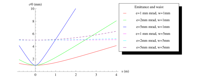
Hence for a 1 mm.mrad beam with a 1 mm spot size, the beam will have increased by 10% beam at s=0.45𝑠0.45s=0.45 m and by 20% at s=0.66𝑠0.66s=0.66m. For the same beam with a 5mm spot size, these distances are multiplied by 25 and become s=11.46𝑠11.46s=11.46m and s=16.6𝑠16.6s=16.6m. Figure 2 gives the beam enveloppes for various emittances and beam waist sizes.
Refer to caption
Figure 2: Beam envelope for different emittance and waist size values. Plain lines are for beams forming a 1 mm waist and dashed lines are for beam forming a 5 mm waist.

1.4 Effect of the scattering in the screens on the beam expansion

An electron traversing nuclear matter will be Coulomb scattered. Most of these scattering will be at very small angle but will add up as the electron progresses through the matter. The phenomena is described in details in [2].

For a bunch of electron, the scattering experienced after traversing a layer of thickness x𝑥x can be approximated by a Gaussian of width[3]:

θ0=13.6 MeVβcpxX0[1+0.038ln(xX0)]subscript𝜃013.6 MeV𝛽𝑐𝑝𝑥subscript𝑋0delimited-[]10.038𝑙𝑛𝑥subscript𝑋0\theta_{0}=\frac{13.6\mbox{ MeV}}{\beta cp}\sqrt{\frac{x}{X_{0}}}\left[1+0.038ln\left(\frac{x}{X_{0}}\right)\right] (6)

where βc𝛽𝑐\beta c is the velocity of the electrons, p their momentum and X0subscript𝑋0X_{0} a quantity called the radiation length and which expresses how high energy electrons loose their energy in a given material111The radiation length is the mean distance over which a high-energy electron looses all but 1/e𝑒e of its energy by Bremstrahlung[2]..

To make it easier to estimate the scattering as a function of the momentum this equation can be rewritten as

pθ0=13.6 MeVβcxX0[1+0.038ln(xX0)]𝑝subscript𝜃013.6 MeV𝛽𝑐𝑥subscript𝑋0delimited-[]10.038𝑙𝑛𝑥subscript𝑋0\displaystyle p\theta_{0}=\frac{13.6\mbox{ MeV}}{\beta c}\sqrt{\frac{x}{X_{0}}}\left[1+0.038ln\left(\frac{x}{X_{0}}\right)\right] (7)

Table 1 shows that the electrons will travel only a small fraction of a radiation length (X0subscript𝑋0X_{0}) in each type of screen considered. A scattering factor pθ0𝑝subscript𝜃0p\theta_{0} of the order of a hundred MeV.mrad means that a beam with an energy of a hundreds MeV will be scattered by about one milliradian. Among the different screens considered, Mylar and Kapton (Polyimide film) introduce the lower scattering and thinner films seems available.

Radiation Thickness Scattering Limit σ0subscript𝜎0\sigma_{0} (eq. 12)
Material Length (X0subscript𝑋0X_{0}) 104X0superscript104subscript𝑋010^{-4}~{}X_{0} pθ0𝑝subscript𝜃0p\theta_{0} 1mm.mradθ01mm.mradsubscript𝜃0\frac{1\mbox{mm.mrad}}{\theta_{0}}
Aluminium (10 μ𝜇\mum) 8.9 cm 1.12 139 MeV.mrad 0.9 mm
Aluminium (30 μ𝜇\mum) 8.9 cm 3.37 242 MeV.mrad 0.5 mm
Mylar (2 μ𝜇\mum) 28.6 cm 0.069 (*) 34 MeV.mrad 3.7 mm
Polyimide film (7.5 μ𝜇\mum) 28.6 cm 0.26 (*) 66 MeV.mrad 1.9 mm
Polyimide film (10 μ𝜇\mum) 28.6 cm 0.34 (*) 77 MeV.mrad 1.6 mm
Mylar (10 μ𝜇\mum) 28.6 cm 0.34 (*) 77 MeV.mrad 1.6 mm
Air (2 m), 1 atm. 3 104superscript10410^{4} cm 66.67 1089 MeV.mrad -
Air (2 m), 0.01 atm. 3 106superscript10610^{6} cm 0.67 (*) 107 MeV.mrad -
Table 1: Nuclear properties of various materials [2] for different thicknesses. (*) Equation 7 is not fully valid at these thicknesses.

When the beam scatters on the screens an additional scattering term is required and equation 1 is approximately modified as follow:

σ(s)=ϵ(β02α0s+γ0s2)+i=1N(s)screens(ssi)θi2𝜎𝑠italic-ϵsubscript𝛽02subscript𝛼0𝑠subscript𝛾0superscript𝑠2subscriptsuperscript𝑁subscript𝑠screens𝑖1𝑠subscript𝑠𝑖superscriptsubscript𝜃𝑖2\sigma(s)=\sqrt{\epsilon(\beta_{0}-2\alpha_{0}s+\gamma_{0}s^{2})}+\sum^{N(s)_{\mbox{screens}}}_{i=1}(s-s_{i})\theta_{i}^{2} (8)

where N(s)screens𝑁subscript𝑠screensN(s)_{\mbox{screens}} is the number of screens located upstream from the position at which the measurement is performed, sisubscript𝑠𝑖s_{i} their position and θisubscript𝜃𝑖\theta_{i} the scattering they induce.

Assuming that all screens are made of the same material with a scattering coefficient θ0subscript𝜃0\theta_{0}, the scattering induced by the first screen will dominate:

i=1N(s)screens(ssi)θi(ss1)θ0similar-to-or-equalssubscriptsuperscript𝑁subscript𝑠screens𝑖1𝑠subscript𝑠𝑖subscript𝜃𝑖𝑠subscript𝑠1subscript𝜃0\sum^{N(s)_{\mbox{screens}}}_{i=1}(s-s_{i})\theta_{i}\simeq(s-s_{1})\theta_{0} (9)

A measurement of the beam size dominated by the term (ss1)θ0𝑠subscript𝑠1subscript𝜃0(s-s_{1})\theta_{0} will provide information on the scattering but not on the emittance of the beam. Hence the screens, their position and the beam optics must be chosen so that in all measurements the scattering can be neglected.

This requires:

ϵσ0s>Nscreensθ0(ss1)italic-ϵsubscript𝜎0𝑠subscript𝑁screenssubscript𝜃0𝑠subscript𝑠1\displaystyle\frac{\epsilon}{\sigma_{0}}s>N_{\mbox{screens}}\theta_{0}(s-s_{1}) (10)

where Nscreenssubscript𝑁screensN_{\mbox{screens}} is the total number of screens used.

Assuming that the first screen is close from the waist and hence ss1ssimilar-to-or-equals𝑠subscript𝑠1𝑠s-s_{1}\simeq s, this can be rewritten as:

ϵσ0>>Nscreensθ0much-greater-thanitalic-ϵsubscript𝜎0subscript𝑁screenssubscript𝜃0\displaystyle\frac{\epsilon}{\sigma_{0}}>>N_{\mbox{screens}}\theta_{0} (11)
σ0<<ϵNscreensθ0much-less-thansubscript𝜎0italic-ϵsubscript𝑁screenssubscript𝜃0\displaystyle\sigma_{0}<<\frac{\epsilon}{N_{\mbox{screens}}\theta_{0}} (12)

Equation 12 can be rewritten as

σ0<<Nscreensϵnγpθ0pmuch-less-thansubscript𝜎0subscript𝑁screenssubscriptitalic-ϵ𝑛𝛾𝑝subscript𝜃0𝑝\displaystyle\sigma_{0}<<N_{\mbox{screens}}\frac{\epsilon_{n}}{\gamma\frac{p\theta_{0}}{p}} (13)
σ0<<Nscreensmcϵnpθ0much-less-thansubscript𝜎0subscript𝑁screens𝑚𝑐subscriptitalic-ϵ𝑛𝑝subscript𝜃0\displaystyle\sigma_{0}<<N_{\mbox{screens}}\frac{mc\epsilon_{n}}{p\theta_{0}} (14)

where ϵnsubscriptitalic-ϵ𝑛\epsilon_{n} is the normalised emittance, γ𝛾\gamma the Lorentz transformation factor and c the speed of light.

This shows that the requirement on σ0subscript𝜎0\sigma_{0} as a function of the normalised emittance and of pθi𝑝subscript𝜃𝑖p\theta_{i} is independent of the beam energy (but the ease of achieving a given σ0subscript𝜎0\sigma_{0} may be different).

At 500 MeV a 7.5μ7.5𝜇7.5\mum polyimide film screen will induce a scattering θi=0.13subscript𝜃𝑖0.13\theta_{i}=0.13mrad. With an emittance ϵ=1italic-ϵ1\epsilon=1mm.mrad, equation 12 requires σ0<<7.6much-less-thansubscript𝜎07.6\sigma_{0}<<7.6mm. The limit value of σ0subscript𝜎0\sigma_{0} as given by equation 12 assuming Nscreens=4subscript𝑁screens4N_{\mbox{screens}}=4 for various screen materials is given in table 1.

When the spot size is chosen so that equation 12 is satisfied the scattering can be neglected, it is the case with thin Mylar or kapton screens .

2 Simulations

2.1 Mathematica

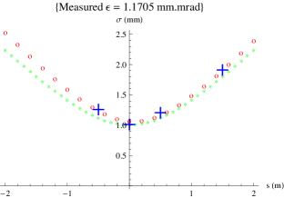
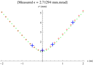
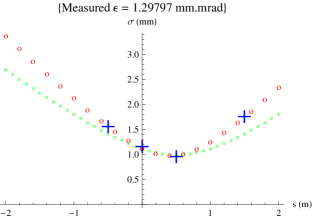
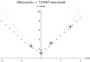
Simple simulations of such measurement have been done using Mathematica. In these simulations 4 screens were positioned at s=0.5m𝑠0.5𝑚s=-0.5m, s=0m𝑠0𝑚s=0m, s=0.5m𝑠0.5𝑚s=0.5m and s=1.5m𝑠1.5𝑚s=1.5m. The propagation of a beam with a given emittance and beta function was then calculated and the size of the beam at each screen was estimated with some noise added. To take into account the limited pixel size the measured beam size was rounded to the size of the pixels.

If the beam optics or the beam energy is not well understood the beam waist may not be positioned exactly where it is expected to be, this was included in our simulations.

Equation 2 was fitted to the beam sizes found and from this fit the value of the emittance was deducted. With the beam sizes used it is assumed that the effect of the scattering can be neglected as the natural beam divergence is much bigger than the divergence induced (equation 12).

Figure 3 shows a few example of such fits.

(a) ϵ=1italic-ϵ1\epsilon=1mm.mrad (b) ϵ=2.5italic-ϵ2.5\epsilon=2.5mm.mrad
s=0𝑠0s=0m s=0𝑠0s=0m
Refer to caption Refer to caption
(c) ϵ=1italic-ϵ1\epsilon=1mm.mrad (d) ϵ=5.1italic-ϵ5.1\epsilon=5.1mm.mrad
s=0.5𝑠0.5s=0.5m s=0𝑠0s=0m
Refer to caption Refer to caption
Figure 3: Simulated (small green dots), measured (blue crosses) and fitted (red circles) beam sizes (σ𝜎\sigma) around the waist. The beam transverse emittance (ϵitalic-ϵ\epsilon) and waist offset (s𝑠s) is indicated above each plot. The waist size is always assumed to be 1 mm and the pixel size 20μm20𝜇𝑚20\mu m. The screens used are assumed to satisfy equation 12 and thus the effect of the scattering is neglected in these plots.

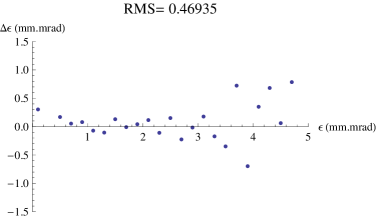
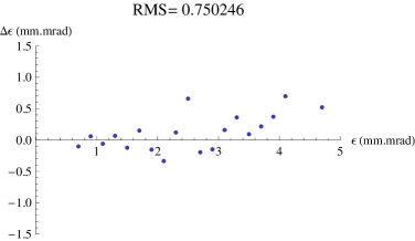
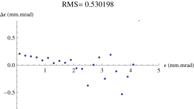
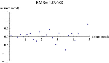
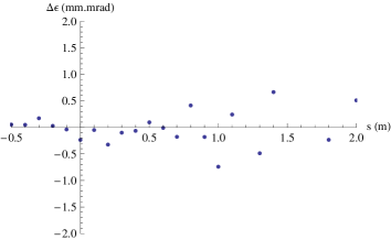
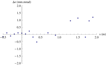
Figure 4 shows the difference between the deducted emittance and the real emittance for several simulation runs.

(a) Pixels = 50 μ𝜇\mum (b) Pixels = 50 μ𝜇\mum
Noise = 5% Noise = 10%
Refer to caption Refer to caption
(c) Pixels = 100 μ𝜇\mum (d) Pixels = 100 μ𝜇\mum
Noise = 5% Noise = 10%
Refer to caption Refer to caption
Figure 4: Error on the emittance measurement as a function of the beam emittance for beams forming a 1 mm waist at s=0𝑠0s=0. In plots (a) and (b) the pixel size is 50 μ𝜇\mum and in plots (c) and (d) it is 100 μ𝜇\mum. For plot (a) and (c) the error on the beam size measurement is 5%, for plot (b) and (d) it is 10%. The screens used are assumed to satisfy equation 12 and thus the effect of the scattering is neglected in these plots.

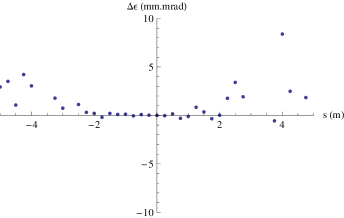
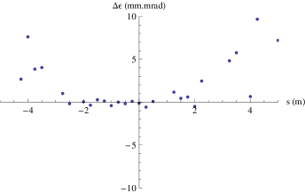
Figure 5 shows the difference between the deducted emittance and the real emittance for several simulation runs where the waist position has been varied. These simulations show when the actual waist is far from s=0𝑠0s=0 the performances of the fit are significantly degraded (this is also visible on figure 3c).

(a) Pixels = 50 μ𝜇\mum (b) Pixels = 100 μ𝜇\mum
Noise = 5% Noise = 10%
Refer to caption Refer to caption
(c) (d)
Refer to caption Refer to caption
Figure 5: Error on the emittance measurement as a function of the position of the beam waist for beams with an emittance of 1 mm.mrad forming a 1 mm waist at the indicated position. In plot (a) and (c) the pixel size is 50 μ𝜇\mum and the noise is 5%. In plot (b) and (d) the pixel size is 100 μ𝜇\mum and the noise is 10%. Plot (c) and (d) repeat plat (a) and (b) over a longer range. The screens used are assumed to satisfy equation 12 and thus the effect of the scattering is neglected in these plots.

2.2 Geant4

To better simulate the effect of the scattering in the screens we have used the Geant4 Toolkit [4].

We have used the Geant Low Energy Physics processes [5]. These processes are valid from 250eV to 100GeV [6] and so completely cover the range of energies we are interested in.

In our simulations the electrons were fired from a source on screens placed 0.5m, 1.0m, 1.5m and 2.5m after the source. The initial direction of the electrons was so that they formed a 2mm waist 1m after the source. A 10μm𝜇𝑚\mu m-thick Mylar window was located 1mm after the electron source.

The position at which the electrons traversed each screen as well as intermediate detectors was recorded. For each simulation more approximately 10 000 electrons were fired.

2.2.1 Effect of the air pressure

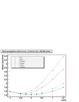
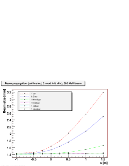
Our first study focused on the effect of scattering in the air contained in the vacuum vessel. The propagation of the beam in the absence of screen in an atmosphere filled with air at different pressures was studied. Figure 6 shows that for pressure higher than 10 mbar the scattering over 2m is significant and thus can not be neglected.
Refer to caption Refer to caption
Figure 6: Scattering experienced by a 500 MeV beam propagating in various air pressure. On the left plot the beam had no initial divergence whereas the beam on the right was focused to make a waist at s=0m with a divergence of 1mrad.

2.2.2 Emittance measurement

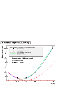
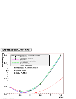
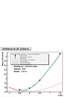
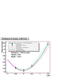
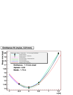
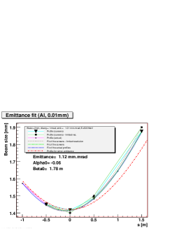
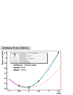
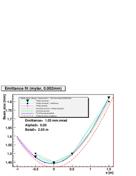
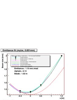
To study the effect of the scattering in the screens several simulations were done using different materials and thicknesses for the screens. Some of the simulations for beams of 200 MeV are shown in figure 7 and for 500 MeV beam in figure 8. As one can see on the figures the use of thin Mylar screens leads to better results than with Aluminium. Furthermore thin Mylar films are easier to handle.
Refer to caption Refer to caption
Figure 7: Scattering induced in a 200 MeV for various screen material and thickness with an initial emittance of 1mm.mrad. The screens material and thickness is given in the plot title. The black squares show the beam size observed on each screen, the black triangles show the beam size rounded to the nearest 50 μm𝜇𝑚\mu m (to simulate what is observed by a camera with a limited pixel size). The open circles are the position measured at additional intermediate positions. The dashed brown line shows the emittance fit made using the black triangles. The dashed green line shows the emittance fit made using the black square. The dashed green line shows the emittance fit made using the open circles. The dashed red line is the theoretical profile of the beam assuming α0=0subscript𝛼00\alpha_{0}=0, β0=2.0msubscript𝛽02.0𝑚\beta_{0}=2.0m and ϵ=1.01mm.mradformulae-sequenceitalic-ϵ1.01𝑚𝑚𝑚𝑟𝑎𝑑\epsilon=1.01mm.mrad. The values given on the plot below the legend for the emittance, α0subscript𝛼0\alpha_{0} and β0subscript𝛽0\beta_{0} are those extracted from the fit on the beam sizes with limited pixel size.
Refer to caption Refer to caption
Figure 8: Scattering induced in a 500 MeV for various screen material and thickness with an initial emittance of 1mm.mrad. The screens material and thickness is given in the plot title. The black squares show the beam size observed on each screen, the black triangles show the beam size rounded to the nearest 50 μm𝜇𝑚\mu m (to simulate what is observed by a camera with a limited pixel size). The open circles are the position measured at additional intermediate positions. The dashed brown line shows the emittance fit made using the black triangles. The dashed green line shows the emittance fit made using the black square. The dashed green line shows the emittance fit made using the open circles. The dashed red line is the theoretical profile of the beam assuming α0=0subscript𝛼00\alpha_{0}=0, β0=2.0msubscript𝛽02.0𝑚\beta_{0}=2.0m and ϵ=1.01mm.mradformulae-sequenceitalic-ϵ1.01𝑚𝑚𝑚𝑟𝑎𝑑\epsilon=1.01mm.mrad. The values given on the plot below the legend for the emittance, α0subscript𝛼0\alpha_{0} and β0subscript𝛽0\beta_{0} are those extracted from the fit on the beam sizes with limited pixel size.

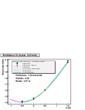
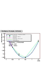
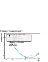
The previous studies assumed that the beam waist was located on the second screen. Figure 9 shows that the emittance can still be reconstructed with a reasonable accuracy when the waist is elsewhere (between the screens).

(a) -0.5m (b) +0.5m (c) +1m
Refer to caption Refer to caption Refer to caption
Figure 9: Scattering induced in a 500 MeV for 10μm10𝜇𝑚10\mu m-thick Mylar screens for a 500 MeV beam with an initial emittance of 1mm.mrad when the waist is not located on the second screen. The waist position is given above the plot. The black squares show the beam size observed on each screen, the black triangles show the beam size rounded to the nearest 50 μm𝜇𝑚\mu m (to simulate what is observed by a camera with a limited pixel size). The open circles are the position measured at additional intermediate positions. The dashed brown line shows the emittance fit made using the black triangles. The dashed green line shows the emittance fit made using the black square. The dashed green line shows the emittance fit made using the open circles. The values given on the plot below the legend for the emittance, α0subscript𝛼0\alpha_{0} and β0subscript𝛽0\beta_{0} are those extracted from the fit on the beam sizes with limited pixel size.

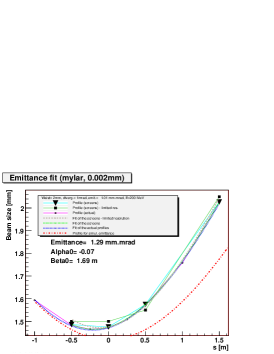
Commercially we found some 2μm2𝜇𝑚2\mu m-thick Mylar coated with a 10nm layer of Aluminium. Neglecting the scattering in the aluminium, the emittance fit can be seen on figure 10.

(a) 200 MeV (b) 500 MeV
Refer to caption Refer to caption
Figure 10: Emittance fit using 2μm𝜇𝑚\mu m-thick Mylar screens at 200 MeV (a) and 500 MeV (b). The black squares show the beam size observed on each screen, the black triangles show the beam size rounded to the nearest 50 μm𝜇𝑚\mu m (to simulate what is observed by a camera with a limited pixel size). The open circles are the position measured at additional intermediate positions. The dashed brown line shows the emittance fit made using the black triangles. The dashed green line shows the emittance fit made using the black square. The dashed green line shows the emittance fit made using the open circles. The dashed red line is the theoretical profile of the beam assuming α0=0subscript𝛼00\alpha_{0}=0, β0=2.0msubscript𝛽02.0𝑚\beta_{0}=2.0m and ϵ=1.01mm.mradformulae-sequenceitalic-ϵ1.01𝑚𝑚𝑚𝑟𝑎𝑑\epsilon=1.01mm.mrad. The values given on the plot below the legend for the emittance, α0subscript𝛼0\alpha_{0} and β0subscript𝛽0\beta_{0} are those extracted from the fit on the beam sizes with limited pixel size.

3 Conclusions

We have studied how 4 screens introduced simultaneously in a beam line could be used to fit the Twiss parameters of an electron beam in a single shot measurement. We have shown that by using 2μm2𝜇𝑚2\mu m-thick Mylar screen such fit would lead to a measurement of the beam transverse emittance correct within 15% for a 500 MeV beam and within 30% for a 200 MeV beam.

References

  • [1] J. Rossbach and P. Schüser. Basic course on accelerator optics. CERN Accelerator School, CERN 94-01, 1994.
  • [2] W. M. Yao et al. Review of particle physics. J. Phys., G33:1–1232, 2006.
  • [3] Gerald R. Lynch and Orin I. Dahl. Approximations to multiple Coulomb scattering. Nucl. Instrum. Meth., B58:6–10, 1991.
  • [4] S. Agostinelli et al. Geant4: A simulation toolkit. Nucl. Instrum. Meth., A506:250–303, 2003.
  • [5] J. Apostolakis et al. Geant4 low energy electromagnetic models for electrons and photons. CERN-OPEN-99-034.
  • [6] S. Chauvie et al. Geant4 low energy electromagnetic physics. Prepared for CHEP’01: Computing in High-Energy Physics and Nuclear, Beijing, China, 3-7 Sep 2001.