Anomalous Transport and Possible Phase Transition in Palladium Nanojunctions
Abstract
Many phenomena in condensed matter are thought to result from competition between different ordered phases. Palladium is a paramagnetic metal close to both ferromagnetism and superconductivity, and is therefore a potentially interesting material to consider. Nanoscale structuring of matter can modify relevant physical energy scales leading to effects such as locally modified magnetic interactions. We present transport measurements in electromigrated palladium break junction devices showing the emergence at low temperatures of anomalous sharp features in the differential conductance. These features appear symmetrically in applied bias and exhibit a temperature dependence of their characteristic voltages reminiscent of a mean field phase transition. The systematic variation of these voltages with zero-bias conductance, together with density functional theory calculations illustrating the relationship between the magnetization of Pd and atomic coordination, suggest that the features may result from the onset of spontaneous magnetization in the nanojunction electrodes. We propose that the characteristic conductance features are related to inelastic tunneling involving magnetic excitations.
Introduction
Many phenomena in modern condensed matter physics, including metal-insulator transitions, high temperature superconductivity, heavy fermions, multiferroic effects, and quantum criticality, are thought to originate from competition between different possible ordered electronic ground states. Slightly shifting the balance between these orders via external fields, strain, disorder, or carrier concentration can tune a system between different phases. Palladium’s proximity to both ferromagnetismFritsche1987 ; Taniyama1997 ; Lee1998 ; Sampedro2003 and superconductivitySkoskiewicz1972 ; Stritzker1972 ; Stritzker1979 make it an interesting material to consider in this context. Structuring matter on the nanometer scale is one means of modifying relevant physical energy scales, with nanoscale confinement already known to favor locally modified magnetic interactions in Pd.Taniyama1997 ; Delin2004 ; Ralph2008 ; Calvo2009 Nanogap structures can be particularly useful in examining the relevant physics in such complicated systems. Tunneling transport has been a valuable spectroscopic tool, with the tunneling conductance as a function of bias voltage typically interpreted as probing the convolution of the electronic densities of states (DOS) of the two electrodes. In fixed nanogap structures, this has given insight into varied systems, including charge density wave compoundsONeill2006 and assorted superconductors.Schmidt2002 ; Ekino1996
In this article we report tunneling measurements in Pd-Pd tunnel junctions fabricated by electromigration of planar constrictions on oxidized Si substrates. We find a characteristic pattern of features in the differential conductance appearing at source-drain voltages () linearly related to the log of the zero-bias conductance (ZBC ). These features rapidly decrease in bias with increasing temperature, with a temperature dependence reminiscent of a mean-field transition. Of particular interest is the contrast in scale between the energy of an individual peak or dip () and the respective temperature at which it vanishes (), which often differ by 100. These features are robust and appear to be particular to Pd electrodes. We discuss possible physical mechanisms for these features, and suggest that they are likely signatures of inelastic tunneling processes associated with the onset of spontaneous magnetization in the electrode tips. While the details have not been definitely determined, calculations of the expected magnetic moment in model Pd nanocontacts are consistent with both the onset temperature of the conductance features and the observed systematic variation of voltage scales with the ZBC.
Results
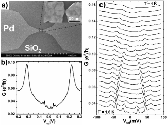
Bowtie-shaped Pd nanowires are fabricated on a Si/SiO2 substrate (see Methods). The devices are cleaned and subsequently cooled to 2 K. A tunneling gap is created in a nanowire by employing the electromigration technique (Fig. 1a).HPark1999 Differential conductance () is measured as a function of , and the conducting substrate is used as a back gate by applying a separate bias, .
When the electromigration process reduces the ZBC below (most commonly between and , where ), a characteristic series of peaks and dips is observed in the curve of vs. when measured at low temperatures. These differential conductance features (DCFs) are highly reproducible in Pd. Out of 111 clean Pd nanowire samples successfully electromigrated to a measurable ZBC less than , more than 75% of devices exhibited characteristic DCFs and their corresponding temperature dependence. This holds true for samples fabricated on both - and -type Si substrates. When the electromigrated nanojunctions have a ZBC of , these features are entirely absent. These DCFs appear to be specific to Pd. Experiments with both Ni-Ni and Au-Au tunnel junctions formed via analogous fabrication processes have shown no indications of similar DCFs.
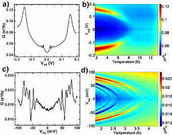
When 1.8 K we distinguish distinct types of DCFs associated with two different bias regimes. In the “low bias” region (typically 110 mV), a series of sharp features appears on each side of = 0 V (Fig. 1b c). From device to device, these peaks and dips occur with varying amplitudes, lineshapes, and spacings; for a given device, the features are clean and reproducible. The “high bias” region (typically 150 mV - 400 mV) contains the second type of feature, which is always manifested as a single pair of relatively broad peaks, with one peak appearing on each side of = 0 V (Fig. 1b). The amplitude of these two peaks is greater than those in the low bias region. While the pattern of all DCFs appear symmetric about = 0 V, there can be an overall asymmetry in conductance magnitudes due to a background contribution (roughly linear in ) to . Such a background is commonly observed in STM and break junction experiments.Nagaoka2002 ; Calvo2009
The DCFs undergo a rapid decrease in voltage position and amplitude as temperature is increased (Fig. 1c). At sufficiently high temperatures all temperature-evolving features have disappeared, and the resulting trace of appears weakly nonlinear, consistent with what is expected for an ordinary metallic break junction device with a small interelectrode gap. A critical temperature, , can be assigned to each DCF, defined as the temperature at which that particular feature approaches = 0 V. The energy of an individual peak or dip cannot usually be tracked all the way to = 0 V as it invariably becomes difficult to resolve with diminishing amplitude, resulting in the apparent “smearing” of the colormaps in the vicinity of the = 0 V axis (Figs. 2, 3, and 4). The energies of the DCFs decrease with temperature in a manner that is well fit by the equation:
| (1) |
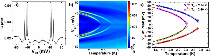
where is the voltage position of the peaks (multiplied by ) as 0 K and , the classical exponent for a mean-field transition in a Landau theory. The low bias DCFs of all Pd devices have 4.3 K and evolve with temperature as in Equation (1). An example is shown in Fig. 3, along with fits to Equation (1). The energy of the high bias peaks also follows this form, but begins to deviate at , where is typically between 8-12 K (Fig. 2b and Supplementary Fig. S5).
In Figure 4 the voltages of representative peaks and dips, from a set of several dozen devices, are plotted as a function of the log of their corresponding ZBC when 1.65 K. The peaks associated with high bias regions are quite linear in log(), indicating that the voltage position of these features decays exponentially with ZBC. Fits to the high bias data indicate that these peaks will go to zero bias as . This is consistent with our observation that DCFs are only present for samples with . DCFs in the plot associated with the low bias regime appear anywhere within a bias range between = 0 V and an upper limit. The edge of this envelope is also roughly linear in the log of .
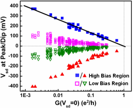
The ZBC of a tunnel junction with a vacuum gap is expected to decrease exponentially with increasing interelectrode gap distance, , according to , where , and is a typical barrier height related to the metal work function. Since log(), a linear relationship exists between the positions of the DCFs and . This is further confirmed by observations in a single device when measurements of vs. are performed after successive electromigrations: The ZBC is reduced and the DCFs are found at higher biases while the pattern of DCFs remains relatively unchanged (see Fig. S2 in Supplementary Information).
Conversion of the ZBC data in Fig. 4 into a distance scale is extremely sensitive to both the conductance prefactor and , neither of which is well established in Pd.Minowa2005 If desired, one could perform theoretical calculations based on density functional theory to obtain a quantitative estimate for with particular tip geometries. A typical value of for vacuum tunneling between high work function metals is 2 Å-1.Wolf1985 Using this value and assuming a prefactor for the conductance of 2 when the two electrodes are in contact at the single atom level, we then estimate that ranges between 1 and 4 Å.
We have also examined the effects of gate bias and magnetic field on the junctions, as further explained in the Supplementary Information. As is increased in the positive (negative) direction, the ZBC decreases (increases), and the DCFs move to higher (lower) energies, increasing (decreasing) their associated ’s (Fig. S1c). Some DCFs appear to split at large negative . There is no sign of Coulomb stability diamonds, and these gate bias effects have the same polarity for both - and -type substrates. External magnetic fields up to 9 T in a direction perpendicular to the plane of the devices lead to no significant effects. There is no Zeeman splitting or broadening of peaks in , and no hysteresis seen in measurements of magnetoresistance (Fig. S1d). There is a very slight shift () of DCFs to higher voltages at 9 T, but we cannot rule out that this is due to slight field-dependent changes in sample temperature. SQUID measurements of co-deposited Pd films show only paramagnetic response down to 2.0 K.
Discussion
Selectively altering matter on the nanometer scale is one means of modifying relevant physical energy scales and can lead to collective electronic effects not necessarily present in bulk samples. The anomalous transport data presented here, found in a chemically homogeneous system, are an example of such an effect. We consider several possible explanations for the observed phenomena. One concern is that the DCFs are extrinsic rather than an inherent property of the Pd junctions. For example, the presence of helium exchange gas in the chamber raises the possibility that an adsorbed He film could be the origin of the features. This is unlikely however, since the DCFs are also observed when no He exchange gas is used. Also, with or without exchange gas, the high bias DCFs survive well above 4.2 K.
Similarly, it is well established that hydrogen has an affinity for Pd.Baykara2004 Previous experiments involving tunneling spectroscopy of metallic nanogaps in the presence of H2 reveals low temperature features reminiscent of our data due to transitions between coverage dependent statesGupta2005 or vibrational modesThijssen2006 of the molecules. The voltages of the DCFs we report are similar in scale to the energy of phonons or vibrational modes related to adsorbed molecules. However, phonon mode energies do not have the strong temperature dependence exhibited by these DCFs. Furthermore, unlike the H2-containing junctions, our devices are stable over time (3-4 days), do not exhibit enhanced noise or telegraph switching, and the DCFs do not appear with highly reproducible energies.Csonka2004
One possible interpretation of the data is that reflects a convolution of the (thermally broadened) DOS of the source and drain electrodes or a particle between the electrodes, as in scanning tunneling spectroscopy. In this situation the DCFs would correspond to features in the DOS at energies away from the Fermi level (). A probe of the electrode DOS would not be expected to produce symmetric features with respect to , nor would there be reason for the peaks to shift towards with increasing . The symmetry of features with respect to , together with the observed gate and temperature dependencies are also inconsistent with expectations of Coulomb blockade physics (e.g., resonant tunneling through a nanoparticle in the interelectrode gap).
Pd can undergo a superconducting phase transition when doped with H Skoskiewicz1972 ; Stritzker1972 or when irradiated with He ions Stritzker1979 to create disorder and lattice strain. The form of the -dependence of the DCFs in our devices is the same as that used to describe the energy gap, , in superconducting materials. The data have some qualitative resemblance to that seen in superconductor-superconductor tunnel junctions. However, as temperature is increased one would expect all peaks to approach a common value of , contrary to the behavior of the DCFs in our Pd break junctions. Moreover, the gap energies inferred from interpreting the DCFs as DOS features are orders of magnitude away from what one would anticipate given the observed s.
Figure 4 imposes a significant constraint on any candidate explanation for the data. It is difficult to construct a scenario in which the energies of features in the DOS vary systematically with interelectrode conductance as observed. In a typical tunnel junction, increasing the electrode separation will reduce the conductance amplitude related to features in the DOS (e.g. from resonant tunneling into accessible states), but should not alter their respective energies. Fig. 4 strongly suggests that the DCFs are not simple DOS resonances.
The linear relationship between DCF and the inferred interelectrode separation suggests the possibility that the DCFs represent physics driven by the interelectrode electric field, . However, any electric field-based mechanism is constrained by the mean field-like temperature dependence seen in Fig. 3.
One candidate mechanism would be electric field control of magnetic ordering, which has been suggested by several groupsDuan2008 ; Ovchinnikov2009 ; Kudasov2007 and demonstrated experimentally in FePd.Weisheit2007 Indeed, hole-doping of Pd with an electric field has been predicted to instigate a transition to ferromagnetism, causing a step-like change in the tunneling current at a given value of applied bias.Kudasov2007 In our structures, the bias across the tunnel junction induces a local (on the scale of the screening length) accumulation of electrons and holes on the facing electrodes, resulting in a raising or lowering of the Fermi level at the surface, respectively. Palladium has a peak in the DOS just below the Fermi level. It is conceivable that a sufficient accumulation of holes could result in the satisfaction of the Stoner Criterion leading to itinerant ferromagnetism at that surface.
However, there are a number of problems with this scenario. For example, this idea fails to account for the symmetry observed in the conductance spectrum about . Which electrode is hole-accumulating depends on the bias polarity. It seems unlikely that the two polarities would result in identical electric field-driven transitions. It is also unclear how such a mechanism would lead to the rich variety of DCFs and their observed dependence on (See Supplementary Information). Furthermore, calculations indicate that the strength of the field necessary to instigate such a transition ( 1 V/Å) would require an applied bias prohibitively high in our devices.Kudasov2007 ; Sun2010 Therefore, we do not think that electric field-driven magnetism is a likely explanation for our observations.
We speculate that the observed DCFs are related to inelastic electron tunneling. An inelastic tunneling origin for the low bias DCFs would naturally explain the observed symmetry in , and the variety of lineshapes could be explained by interference between various elastic and inelastic channels involving local modes.Mii2003 ; Galperin2004 In contrast, the high bias DCFs are exclusively broad maxima, suggesting that different processes may be involved for low and high bias features. However, the fact that both regimes are strongly correlated with one another (Fig. 4) and have the same trend with zero-bias conduction strongly implies that the low and high bias DCFs share crucial underlying physics.
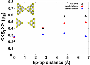
We further propose that the relevant transport channels may arise due to the onset of spontaneous magnetization at the electrode tips due to the proximity of Pd to a magnetic instability. While Pd surfaces are not magnetic for film thicknesses exceeding a few monolayers, reports suggest the possibility of itinerant ferromagnetism in Pd nanoparticles,Lee1998 ; Sampedro2003 and atomic-size contacts.Delin2004 Zero-temperature density functional theory (DFT) calculations for model Pd nanocontacts, as those shown in Fig. 5, indicate the possible presence of magnetism due to the low coordination of the atoms forming the electrode tips. (See Supplementary Information for calculation details). A quantitative estimate of the Curie temperature is, however, beyond DFT capabilities. Furthermore, even if we take the calculated energy difference per atom between the ferromagnetic and paramagnetic states as a reference value, the inherent uncertainties in the calculations are larger than the range of the observed DCF s. Nevertheless, we can say that this energy difference sets an upper limit to that is consistent with the observed values (see Supplementary Information).
If one assumes an excitation energy proportional to the local magnetization (consistent with, e.g., Stoner excitations), then the temperature evolution of would correspond to the onset of magnetic order. Moreover, within that assumption the same model calculations are consistent with the trend of Fig. 4. The layer-by-layer magnetic moment per atom (averaged over layer), , is plotted in Fig. 5 for the three atomic end layers of one tip (the other tip is identical) as a function of the distance between tips, . The calculated average magnetic moment per atom decreases as one moves away from the ends of the tips towards the bulk, revealing the expected inhomogeneous nature of the magnetization. The magnetic moment of the tip atom is visibly affected by the interelectrode distance, decreasing with below 5 Å, consistent with the dynamic range of estimated earlier from the measured ZBC. This can be rationalized by noting that on increasing the coordination (decreasing ) the DOS decreases at the Fermi level and the polarization becomes weaker, in accord with the Stoner criterion. The electrodes in a real break junction may contain many undercoordinated atoms, giving rise to localized areas of increased magnetic susceptibility, extending over a larger region of the junction. In this picture, DCFs with different s would result from different local portions of the electrodes.
Another related speculative mechanism for DCFs involves the interplay of spontaneous magnetization, as above, and Kondo physics. The formation of the highly correlated Kondo state in bare metal break junction devicesRalph1992 ; Houck2005 can lead to sharp features in at symmetric voltages. In this case the peaks would correspond to a spin-split zero-bias resonance resulting from a strong local exchange field established by the presence of ferromagnetismPasupathy2004 ; Calvo2009 or effective magnetic impurities.Heersche2006 The -dependent onset of local magnetization at the electrode tips could lead to such a splitting that increases with decreasing temperature.
The apparent lack of magnetic hysteresis and significant magnetoresistive effects would seem to cast doubt on a hypothesis involving magnetic correlations. However, it is worth recalling that Stoner-like excitations would not Zeeman split, although they may be expected to shift with the application of an external magnetic field. Furthermore, magnetically ordered regions possibly present very small local anisotropy energiesWierzbowska2005 and a superparamagnetic response to externally applied fields. This implies a vanishingly small coercivity and suggests that large hysteretic effects are not necessarily expected.Skumryev2003 The mismatch between DCF energy scale and is not readily explained, and would require a more detailed theoretical picture of the inferred magnetic transition and resulting excitations. One should recall, however, that Stoner excitations (invoked as a possible explanation of DCFs) and the spin stiffness (related to ) are associated with different exchange couplings.Pajda2001 This makes their characteristic energy scales differ by an order of magnitude, at least in transition metals. We see no reason to expect otherwise in the case of Pd.
The data presented here unambiguously show that unusual electronic effects are present in Pd nanojunctions at low temperatures. The trends in the data with , , , and greatly restrict possible mechanisms. While speculative, an explanation of the features in terms of inelastic processes involving magnetism is consistent with the observed temperature range, source-drain symmetry, special character of Pd, and the trend with inferred electrode separation. This idea is also testable through doping the Pd with a ferromagnetic metal to see if enhancing the tendency toward ferromagnetism alters the phenomenon. These conductance anomalies demonstrate once again that even “simple” chemically homogeneous materials can exhibit rich and surprising phenomena at the nanoscale.
Methods Arrays of bowtie-shaped nanowire patterns are defined by electron beam lithography with minimum widths between 80 and 100 nm. Samples are composed of 14 nm of Pd deposited by e-beam evaporation on a highly doped Si substrate with a 200 nm SiO2 insulating layer (Fig. 1a). The devices are contacted individually using a piezo-controlled Attocube™probe station inside of a 4He cryostat. An array of devices is cleaned in solvents, exposed to an oxygen or argon plasma clean, and subsequently inserted into the sample space of the probe station, which contains approximately 10 mB of He exchange gas at 300 K. The electromigration techniqueHPark1999 is employed at low temperature ( 2 K) to create a small gap in the nanowire (Inset, Fig. 1a). Differential conductance () is measured as a function of source-drain bias () using standard low frequency lock-in techniques with an rms excitation voltage of 625 V. I-V is also measured using a voltage source and current preamplifier, for a small portion of samples.
Acknowledgment. D.N. acknowledges support from the David and Lucille Packard Foundation and the W. M. Keck Foundation. G.D.S. acknowledges the support of the W. M. Keck Program in Quantum Materials at Rice University. The authors would like to thank Joaquín Fernández-Rossier, David Jacob, Qimiao Si, Jan van Ruitenbeek, Christian Schönenberger, Michel Calame, Nadya Mason, Allen Goldman, and Laura Greene for comments and discussions, Dan Ward for assistance with SEM images, and Emilia Morosan and Liang Zhao for SQUID measurements.
Supplementary Information Available. This includes additional details with regard to experimental setup and results not included in the main text. The effect of an applied gate bias is addressed as well as results pertaining to tests performed in the presence of hydrogen gas. Lastly we address the details of the DFT calculations.
References
- (1) Fritsche, L.; Noffke, J.; Eckard, H. A Relativistic Treatment of Interacting Spin-Aligned Electron Systems: Application to Ferromagnetic Iron, Nickel and Palladium Metal. J. Phys. F: Met. Phys. 1987, 17, 943-965.
- (2) Taniyama, T.; Ohta, E.; Sato, T. Observation of 4d Ferromagnetism in Free-Standing Pd Fine Particles. Europhys. Lett. 1997, 38, 195-200.
- (3) Lee, K. Possible Magnetism in Small Palladium Clusters. Phys. Rev. B 1998, 58, 2391-2394.
- (4) Sampedro, B.; Crespo, P.; Hernando, A.; Litrán, R.; Sánchez López, J. C.; López Cartes, C.; Fernandez, A.; Ramírez, J.; González Calbet, J.; Vallet, M. Ferromagnetism in fcc Twinned 2.4 nm Size Pd Nanoparticles. Phys. Rev. Lett. 2003, 91, 237203.
- (5) Skoskiewicz, T. Superconductivity in the Palladium-Hydrogen and Palladium-Nickel-Hydrogen Systems. Phys. Stat. Sol. (a) 1972, 11, K123-K126.
- (6) Stritzker, B.; Buckel, W. Superconductivity in the Palladium-Hydrogen and the Palladium-Deuterium Systems. Z. Physik 1972, 257, 1-8.
- (7) Stritzker, B. Superconductivity in Irradiated Palladium. Phys. Rev. Lett. 1979, 42, 1769-1773.
- (8) Delin, A.; Tosatti, E.; Weht, R. Magnetism in Atomic-Size Palladium Contacts and Nanowires. Phys. Rev. Lett. 2004, 92, 057201.
- (9) Kuemmeth, F.; Bolotin, K. I.; Shi, S.; Ralph, D. C. Measurement of Discrete Energy-Level Spectra in Individual Chemically Synthesized Gold Nanoparticles. Nano Lett. 2008, 8, 4506-4512.
- (10) Calvo, M. R.; Fernández-Rossier, J.; Palacios, J. J.; Jacob, D.; Natelson, D.; Untiedt, C. The Kondo Effect in Ferromagnetic Atomic Contacts. Nature 2009, 458, 1150-1153.
- (11) O Neill, K.; Slot, E.; Thorne, R. E.; van der Zant, H. S. J. In-Chain Tunneling Through Charge-Density-Wave Nanoconstrictions and Break Junctions. Phys. Rev. Lett. 2006,96, 096402.
- (12) Schmidt, H.; Zasadzinski, J. F.; Gray, K. E.; Hinks, D. G. Evidence for Two-Band Superconductivity from Break-Junction Tunneling on MgB2. Phys. Rev. Lett. 2002, 88, 127002.
- (13) Ekino, T.; Fujii, H.; Kosugi, M.; Zenitani, Y.; Akimitsu, J. Tunneling Spectroscopy of the Superconducting Energy Gap in RNi2B2C(R=Y and Lu). Phys. Rev. B 1996, 53, 5640-5649.
- (14) Park, H.; Lim, A. K. L.; Alivisatos, A. P.; Park, J.; McEuen, P. L. Fabrication of Metallic Electrodes with Nanometer Separation by Electromigration. Appl. Phys. Lett. 1995, 75, 301-303.
- (15) Nagaoka, K.; Jamneala, T.; Grobis, M.; Crommie, M. F. Temperature Dependence of a Single Kondo Impurity. Phys. Rev. Lett. 2002, 88, 077205.
- (16) Minowa, T.; A. Fujii, A.; Takeda, M.; Kurokawa, S.; Sakaib, A. Conductance of Pd Single-Atom Contacts. App. Surf. Sci. 2005, 241, 14-17.
- (17) Wolf, E. L. Principles of Electron Tunneling Spectroscopy; Oxford University Press: New York, and Clarendon Press: Oxford, 1985.
- (18) Baykara, S. Z. Theoretical Evaluation of Diffusivity of Hydrogen in Palladium and Rhodium. Int. J. of Hydrogen Energy 2004, 29, 1631-1636.
- (19) Gupta, J. A.; Lutz, C. P.; Heinrich, A. J.; Eigler, D. M. Strongly Coverage-Dependent Excitations of Adsorbed Molecular Hydrogen. Phys. Rev. B 2005, 71, 115416.
- (20) Thijssen, W. H. A.; Djukic, D.; Otte, A. F.; Bremmer, R. H.; van Ruitenbeek, J. M. Vibrationally Induced Two-Level Systems in Single-Molecule Junctions. Phys. Rev. Lett. 2006, 97, 226806.
- (21) Csonka, Sz.; Halbritter, A.; Mihály, G. Conductance of Pd-H Nanojunctions. Phys. Rev. Lett. 2004, 93, 016802.
- (22) Duan, C. G.; Velev, J. P.; Sabirianov, R. F.; Zhu, Z. Q.; Chu, J. H.; Jaswal, S. S.; Tsymbal, E. Y. Probing Superexchange Interaction in Molecular Magnets by Spin-Flip Spectroscopy and Microscopy. Phys. Rev. Lett. 2008, 101, 137201.
- (23) Weisheit, M.; Fahler, S.; Marty, A.; Souche, Y.; Poinsignon, C.; Givord, D. Electric Field-Induced Modification of Magnetism in Thin-Film Ferromagnets. Science, 2007, 315, 349-351.
- (24) Ovchinnikov, I. V.;, Wnag, K. L. Theory of Electric-Field-Controlled Surface Ferromagnetic Transition in Metals. Phys. Rev. B, 2009, 79, 020402(R).
- (25) Kudasov, Yu. B.; Korshunov, A. S. Surface Ferromagnetism of Palladium Induced by Strong Electric Field. Phys. Lett. A 2007, 364, 348-351.
- (26) Sun, Y.; Burton, J. D.; Tsymbal, E. Y. Electrically Driven Magnetism on a Pd Thin Film. Phys. Rev. B 2010, 81, 064413.
- (27) Mii, T.; Tikhodeev, S. G.; Ueba, H. Spectral Features of Inelastic Electron Transport via a Localized State. Phys. Rev. B 2003, 68, 205406.
- (28) Galperin, M.; Ratner, M. A.; Nitzan, A. Inelastic Electron Tunneling Spectroscopy in Molecular Junctions: Peaks and Dips. J. Chem. Phys. 2004, 121, 11965-11979.
- (29) Ralph, D. C.; Buhrman, R. A. Observations of Kondo Scattering Without Magnetic Impurities: A Point Contact Study of Two-level Tunneling Systems in Metals. Phys. Rev. Lett. 1992, 69, 2118-2121.
- (30) Houck, A. A.; Labaziewicz, J.; Chan, E. K.; Folk, J. A.; Chuang, I. L. Kondo Effect in Electromigrated Gold Break Junctions. Nano. Lett. 2005, 5, 1685-1688.
- (31) Pasupathy, A. N.; Bialczak, R. C.; Martinek, J.; Grose, J. E.; Donev, L. A. K.; McEuen, P. L.; Ralph, D. C. The Kondo Effect in the Presence of Ferromagnetism. Science, 2004, 306, 86-89.
- (32) Heersche, H. B.; de Groot, Z.; Folk, J. A.; Kouwenhoven, L. P.; van der Zant, H. S. J.; Houck, A. A.; Labaziewicz, J.; Chuang, I. L. Electron Transport Trough Single Mn12 Molecular Magnets. Phys. Rev. Lett. 2006, 96, 017205.
- (33) Wierzbowska, M.; Delin, A.; Tosatti, E. Effect of Electron Correlations in Pd, Ni, and Co Monowires. Phys. Rev. B 2005, 72, 035439.
- (34) Skumryev, V.; Stoyanov, S.; Zhang, Y.; Hadjipanayis, G.; Givord, D.; Nogués, J. Beating the Superparamagnetic Limit with Exchange Bias. Nature 2003, 423, 850-853.
- (35) Pajda, M.; Kudrnovský, J.; Turek, I.; Drchal, V.; Bruno, P. Ab Initio Calculations of Exchange Interactions, Spin-Wave Stiffness Constants, and Curie Temperatures of Fe, Co, and Ni. Phys. Rev. B 2001, 64, 174402.