shallow donor near a semiconductor-metal and a semiconductor-dielectric interface
Abstract
The ground state energy and the extend of the wavefunction of a negatively charged donor () located near a semiconductor-metal or a semiconductor-dielectric interface is obtained. We apply the effective mass approximation and use a variational two-electron wavefunction that takes into account the influence of all image charges that arise due to the presence of the interface, as well as the correlation between the two electrons bound to the donor. For a semiconductor-metal interface, the binding energy is enhanced for donor positions ( is the effective Bohr radius) due to the additional attraction of the electrons with their images. When the donor approaches the interface (i.e. ) the binding energy drops and eventually it becomes unbound. For a semiconductor-dielectric (or a semiconductor-vacuum) interface the binding energy is reduced for any donor position as compared to the bulk case and the system becomes rapidly unbound when the donor approaches the interface.
pacs:
73.20.-r, 71.55.-i, 73.20.HbI Introduction
The negatively charged donor center, also called system (a hydrogenic donor with a second electron bound to it) has received a lot of interest in the past both from researchers in astrophysics (where it is known as the H- ion Chand ) and semiconductor physics Hill . Furthermore, the center is one of the simplest “many-body” electronic system that can also be used as a model system to test how well certain theories are able to include electron-electron (e-e) correlations. It has been shown that in the absence of electric and magnetic fields the has only one bound state Hill . Experimentally, states have been observed in bulk semiconductors ExpBulkSemi , in quantum wells ExpQW , and in superlattices Huant . Tunneling through the state was reported in Ref. Lok, for a confined in a double-barrier resonant tunneling device. The resonance appears in addition to the known resonance due to tunneling through the ground state of the neutral donor . It was found that in high magnetic fields the amplitude of the resonant peak becomes significantly larger as compared to the amplitude of the peak Lok .
Theoretically, the center has been investigated using the variational method within the effective mass approach: i) for the bulk case Larsen1 , ii) the two-dimensional case Larsen2 ; Larsen3 , and iii) for the superlattice case Shiprb . In a double-quantum-well device a neutral donor at the center of the quantum well in the presence of magnetic field can bind a second electron in the other well (a spatially separated center) as shown in Ref. IKM . In the case of the remote center, where donor and electrons are located in different quantum wells, strong electron-electron correlations can give rise to magnetic-field-induced angular-momentum transitions IKM ; Riva . It has been predicted that electron-phonon interaction in a weakly polar semiconductor leads to a substantial increase of the binding energy Shiprb2 . The negatively charged donor center was used as an approximate model system for a trion (charged exciton) to explain the experimental behavior of the two-dimensional electron gas in a quantum well in high magnetic field at high-laser power Hayne .
In the last years, there has been renewed interest in the study of dopants in semiconductors due to the possibility to dope the material in a controlled way and to tailor the electronic properties in order to create new functional devices. Because of the increased miniaturization, the dopant atoms appear closer and closer to interfaces Koenraad . Recently, using STM, the binding energy of individual dopants close to a semiconductor interface was measured and found to be substantially increased Koenraad . In a recent transport experiment on a nanowire surrounded by a metallic gate it was suggested Sellier that signatures of the state were observed. Due to the closeness of the metallic gate to the donor it was argued that the metallic gate screens the repulsive e-e interaction which should lead to a larger binding energy. Here we will show that this expectation is only correct if the donor is not too close to the interface. For very close proximity of the donor to the interface the binding energy drops and can even become negative, i.e. unbound system. A second motivation for the present study is that the system can serve as an entangled pair of electrons which currently is of great interest for quantum information applications Bao . The quantum control of a near a semiconductor-dielectric interface and its possible application for quantum computing has been discussed in Ref Calderon .
In this paper we study the spin-singlet state of a system near a semiconductor-metal (and semiconductor-dielectric) interface within the effective mass approach. As compared to the 3D situation the present problem differs in the following two aspects: 1) the many-particle wavefunction is zero at the interface, and 2) due to the dielectric mismatch at the interface image charges are induced that results in a complicated multi-center Coulomb problem. For the ground state trial function we used a Chandrasekhar type space symmetric wave function which we modified in order to satisfy the boundary condition on the semiconductor-insulator interface, and to take into account the contribution of the Coulomb interaction with the image charges in the system. To describe the interaction of the electrons with the images in the insulator or in the metallic gate, we add additional terms to the Chandrasekhar trial function Chand . For the case of a single electron bound to a donor near a metallic or dielectric interface, i.e. the problem, similar terms were introduced recently in Ref. Hao, which we modified slightly in order to obtain even better results for . In the present paper, we have calculated the ground state energy of the system as a function of the donor position with respect to a semiconductor-metal, a semiconductor-dielectric and a semiconductor-vacuum interface.
The present paper is organized as follows. In Sec. II we present the two electron Hamiltonian and propose trial wave functions for the center. In Sec. III the ground state energy of the center near different interfaces is studied as a function of the position of the donor. The extend of the wavefunction and its average position in the direction parallel and perpendicular to the interface were also calculated. Our conclusions and a summary of our results are presented in Sec. IV.
II The formalism and the variational wave function
The Hamiltonian of the system, consisting of a donor at a position near a semiconductor-metal (semiconductor-dielectric) interface and two electrons is, in cylindrical coordinates, given by the expression
| (1) |
where
| (2) |
is the Hamiltonian of a neutral center near an interface, with
| (3) |
the Coulomb interaction terms and where dimensionless units of the effective Bohr radius and twice the effective Rydberg energy were used and is the ratio between the transverse and longitudinal effective mass (in our numerical calculations we assume ).
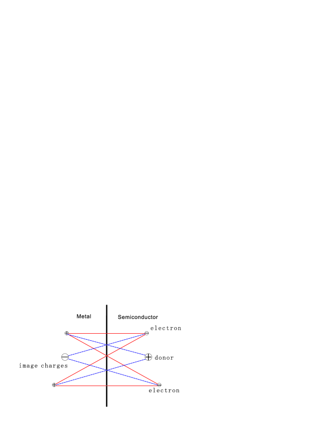
The first term in describes the interaction between an electron and its image, the second arises due to the attractive interaction between an electron and the donor, and the third term is due to the interaction between an electron and the donor image (as well as the donor and the electron image). See Fig. 1 for a schematic representation of the different Coulomb terms in case of a semiconductor-metal interface for which (i.e. ). In Eq. (3) the image charge is given by with () the permittivity of the semiconductor (dielectric). For the case of a semiconductor-metal interface we assume a very thin oxide layer between the semiconductor and the metal and its only effect is to prevent the electron to penetrate into the metal, i.e. it provides a very high potential barrier. The two-electron Coulomb potential has the following form
| (4) |
with
| (5a) | |||
| (5b) |
where describes the electron-electron interaction and is the interaction between an electron and the image of the other electron.
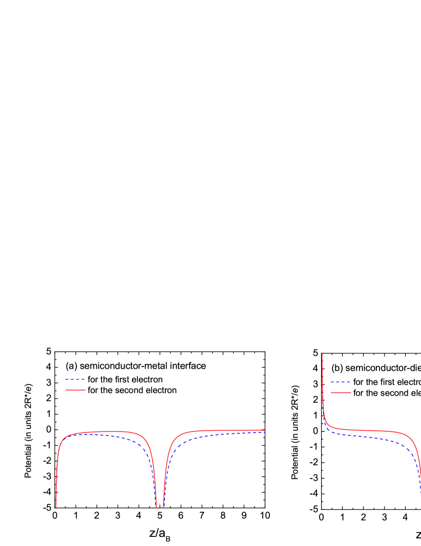
The potential energy for the electron along the -direction for is shown by the dashed curve in Fig. 2(a) for the semiconductor-metal interface and in Fig. 2(b) for the semiconductor-dielectric interface. The electron is subject to a Coulomb potential near the donor and the potential due to the image charges. When an electron is bound to the positive donor the system becomes neutral and this electron will screen the donor Coulomb potential for a second electron. The mean-field potential seen by the second electron is given by
| (6) |
where is the normalized ground-state wavefunction of the electron which we obtained previously in Ref. Hao, . This potential is plotted in Figs. 2(a,b) by the solid curve and it is immediately clear that the second electron will feel a strongly screened donor potential. The Coulomb potential is replaced Larsen2 by the screened potential . As a result the second electron can at most only be very weakly bound. Solving this mean-field problem for the second electron will strongly underestimate the binding energy because it neglects: i) exchange, and ii) electron-electron correlation. The latter will lead to a polarization of the neutral system.
In order to account for exchange and correlation we introduce a Chandrasekhar type space symmetric wave function (because we consider the spin single state, i.e. ) which also takes into account the interaction with the image charges in the system, and satisfies the boundary condition at the interface:
| (7) |
where
| (8a) | ||||
| (8b) | ||||
| (8c) |
with the distance between the electron and the donor, is the distance between the two electrons and is a normalization constant. In our previous work Hao on the neutral donor problem we found that introducing an asymmetry in , i.e. , with an extra variational parameter, improved the binding energy only with 2.7% for and with less than 1% for . Therefore, in order to limit the number of variational parameters we took . The factor in front of the wave function (7) guarantees that the boundary condition is satisfied for each electron and that for large -values the 3D result can be recovered (because then approach the constant value ). The wave function contains 6 variational parameters: , , , , and . The symmetric combination of hydrogen-like factors in Eq. (8b), takes into account the interactions of the two electrons with the donor, as was proposed in Ref. Chand, , and describes the electron-electron correlation. We introduced the combination of exponential factors that describes the overall interaction of each electron with its image, as well as with the images of the donor and the other electron. Similar functions for the electron-electron repulsive interaction (but with ) were used previously for the system in quantum wells Shiprb and for the two-electron parabolic quantum dot Avetisjpm .
For a neutral electron-donor problem near an interface Hao we took and thus which resulted in very good agreement between the results of the variational method and a numerical ’exact’ finite-element solution. Although the energy was found to be accurate it is clear that the bulk wavefunction is not recovered for , which should be spherical symmetric around the donor. This is the reason why we introduced which for approaches the constant value and makes the wavefunction spherical symmetric. In Table 1 we compare the obtained variational energy for the using and ; we see that the latter gives lower energy for all -values. Thus this extra variational parameter has only a small influence on the energy (we checked that the same conclusion holds for the problem). But we found that quantities as, e.g., the average electron position behave much better at large if we include as a variational parameter. For we have and our variational wavefunction reduces to the one proposed by Chandrasekar Chand which has been shown to result in accurate values for the bulk binding energy.
| asymmetric e-e | |||
|---|---|---|---|
| 2 | -0.40883 | -0.41464 | -0.41464 |
| 3 | -0.49106 | -0.49783 | -0.49783 |
| 4 | -0.51680 | -0.52180 | -0.52186 |
| 5 | -0.52518 | -0.52885 | -0.52891 |
| 6 | -0.52768 | -0.53061 | -0.53067 |
| 7 | -0.52811 | -0.53059 | -0.53063 |
| 8 | -0.52787 | -0.52998 | -0.53001 |
| 9 | -0.52747 | -0.52922 | -0.52924 |
| 10 | -0.52709 | -0.52850 | -0.52852 |
Due to the presence of the interface the e-e correlation term is not necessarily circular symmetric. In order to check the influence of this asymmetry on the energy we introduced an additional variational parameter in the e-e correlation part of Eq. (7),
| (9) |
The ground state energy of the near a semiconductor-metal interface calculated by using in the wavefunction Eq. (7) is presented in the last column of Table 1. Notice that allowing the e-e correlation to be anisotropic does not have a significant influence on the energy, the differences between the energy calculated with or without are very small (less than 0.02%). Therefore, in the following we did not include in our calculations.
The binding energy is defined as follows:
| (10) |
where is the ground state energy of the system Hao . Eq. (10) gives the energy that is needed to remove one of the electrons from the donor to infinity. This definition corresponds to the one used for a 3D system. For a metallic interface, another definition of the binding energy can be used:
| (11) |
where is the binding energy of an electron with its image near a metallic interface Hao ; Loudon . This is the energy needed to remove one electron from the and bring it to the interface.
The expectation values for the position of electron in the -direction and in the plane are calculated as and , respectively, using only the first part in the total trial function, i.e. . This allows us to discriminate between the two electrons, one is closely bound to the positive impurity while the other one is very weakly bound. Notice that thanks to our variational wavefunction we are able to separate ’artificially’ the two electrons. But the variational wavefunction itself considers the two electrons to be indistinguishable because .
III The ground state energy of the center
A. Semiconductor-metal interface
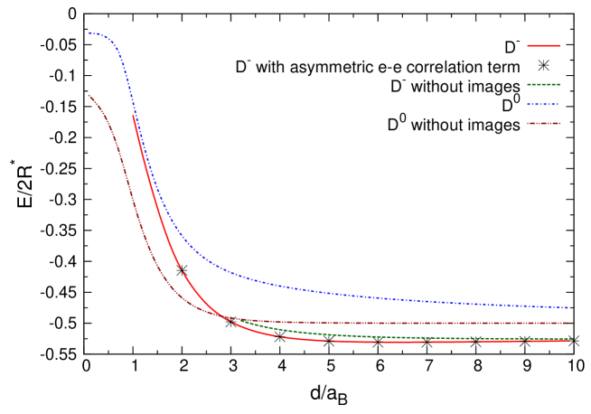
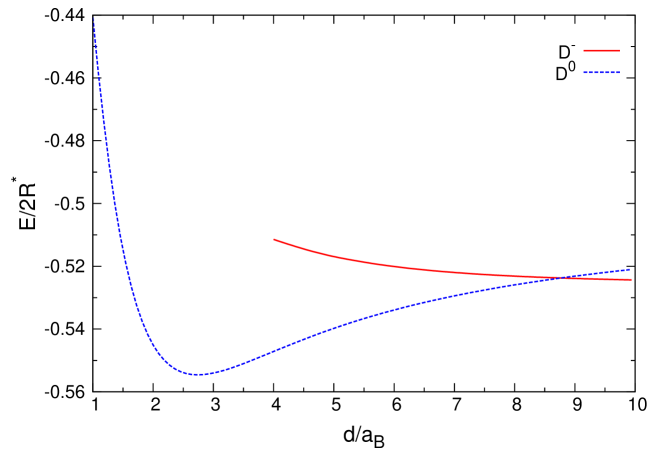
The ground state energy, in units of , is shown in Fig. 3 as a function of the distance of the donor from the interface . The energy exhibits a shallow minimum around and approaches the bulk result from below for . For the energy is a decreasing function of which is mostly a consequence of the extra constraint that the wavefunction has to be zero at the interface. This can be inferred from the result without image charges (dashed green curve in Fig. 3). The outer electron of the center becomes bound for . We considered the second electron bound if the variational parameter is larger than zero and the average position of the electron is not too far from the donor, i.e. . For a semiconductor-metal interface, we have two positive image charges from the electrons and only one negative image charge from the donor, so a strengthened electron bound state is expected. This is confirmed by the fact that if we ignore the image charges the second electron becomes only bound when (see the dashed green curve in Fig. 3).
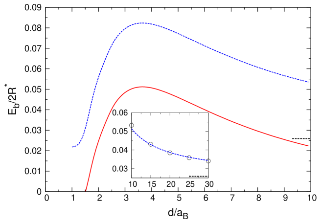
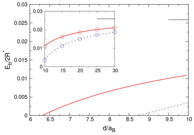
The binding energy is plotted in Fig. 4 using the two different definitions of the binding energy (Eqs. (10) and (11)). A clear maximum is found for beyond which the binding energy slowly decreases to its value. This algebraic decrease is due to the interaction with the image charges and is largely a consequence of the -dependence of the energy. For the definition of the binding energy with (blue dashed curve in Fig. 4) the bulk binding energy is reached from above. Notice that for , which is a factor 3.18 larger than the bulk binding energy. The large -range is shown in the inset and we found that it can be fitted by the curve .
It is remarkable that in the case the effect of the image charges on its energy almost cancels out for intermediate , while this is not so for the neutral system. In our previous work Hao we found that in the case of a semiconductor-metal interface the contribution of the image terms to the energy of a neutral center is given by for large . This is the sum of the contributions arising due to the interaction of the electron with its image (about ) and the interactions of the electron with the donor image as well as the electron image with the donor (each one is about ). In Fig. 1 we show by dashed lines the repulsive interactions between the electrons and the donor image as well as between the donor and the images of the electrons (each line is characterized by the Coulomb energy ) and by solid lines the attractive interactions between the electrons and their images (each with the energy ). Now, in the case of the , due to the presence of the two electrons (see Fig. 1), we have twice the energy shift of the single electron problem , and there is also twice a negative shift due to the interaction of each electron with the image of the other electron (see Eq. (5b)). As a result these energy shifts compensate each other, and we find that the energy for is equal to the energy of the without image charges and is very close to the energy of in the bulk Chand . The same compensation takes place in the case of a semiconductor-dielectric interface where the large contribution of image terms in the energy of the neutral D0 center is about
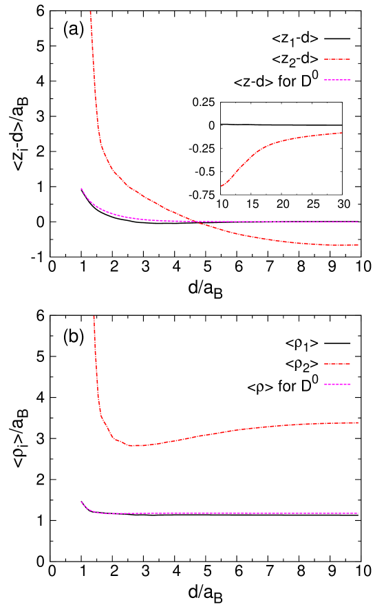
The average position of the electrons in the -direction and their extend in the plane parallel
to the interface are shown in Figs. 5(a) and 5(b),
respectively. Notice that one of the electrons, also called the inner electron, follows very
closely the behavior of the electron bound in the neutral system. This is very similar to
what was found previously for the case of a bulk Larsen1 . The second electron, called
the outer electron, is more extended in the -plane, i.e. its average value is about three times larger than for the inner electron. Notice that for the outer electron increases rapidly with decreasing when signaling a
rapid decrease of the binding energy and ultimately an unbinding of the outer electron. For
the outer electron is attracted towards the interface, i.e. ,
as a consequence of the image charges which is responsible for the enhanced binding energy.
For smaller values we have and the outer electron is pushed away from
the interface mostly as a consequence of the boundary condition at the interface. This behavior is
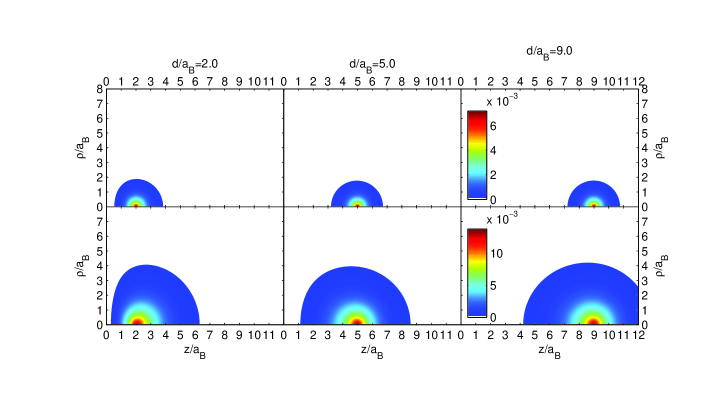
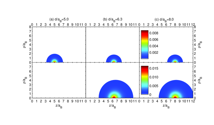
also illustrated in Fig. 6 where we show the contour plots of the electron
density of the outer and inner electron, i.e. with ,
and taken as their average value, for , 5, 9. Notice that the
electron distribution is asymmetric when the donor is close to the interface and that in such a
case a large part of the distribution is found with . In order to illustrate the effect of
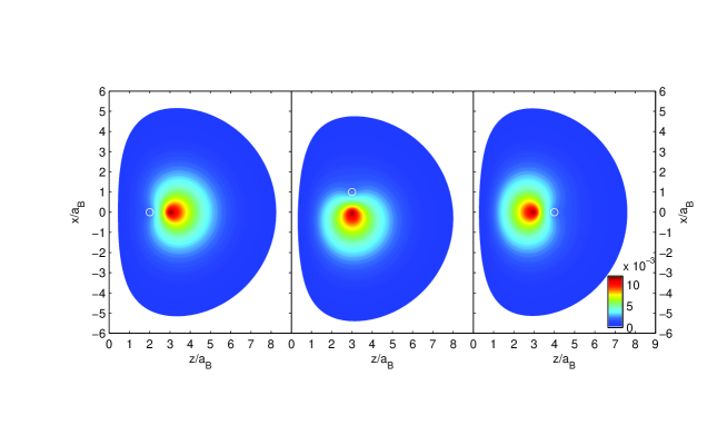
the electron-electron correlation we show in Fig. 7 the conditional
probability . This is the probability
to find an electron at position when the other electron is fixed at position
. We fix one of the electrons close to the donor (i.e. it is the inner electron) and
put it in three different positions with respect to the interface-donor axis. Notice that the
electron: 1) has the highest probability to be close to the donor, 2) it is repelled by the fixed
electron, and 3) it has a non-zero probability to be located at . The reason is that
the two electrons have opposite spin and therefore the Pauli exclusion principle is not
applicable.
B. Semiconductor-dielectric interface
In this subsection we investigate the ground state energy of a center near a semiconductor-dielectric interface. We used material constants for the semiconductor side corresponding to (Si) and for the oxide side (SiO2).
The potential energy between the particles is still given by Eq. (1) with corresponding
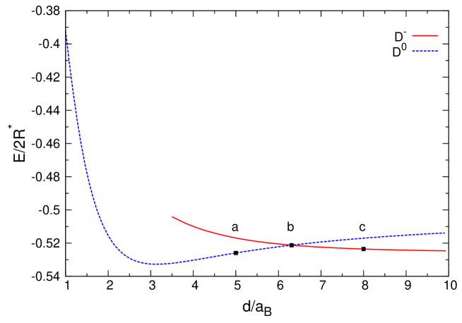
value of . The results are presented in Fig. 8 for the ground state energy
and in Fig. 9 for the binding energy. The second electron is bound to
the for which compares to when we ignore the image charges. This
can be explained by the fact that for the system near a semiconductor-dielectric interface
the two electrons induces two negative image charges while they are only attracted by one positive
image charge coming from the donor. In Fig. 8 we show also the energy of the by
the dashed blue curve which corresponds to the situation where the second electron is at infinity.
Notice that both curves cross at and for smaller -values the state has a
higher energy and consequently the second electron will be unbound. The binding energy of the
second electron to the is plotted in Fig 9 by the solid red curve.
This result approaches the bulk result slowly and from below. The inset of
Fig. 9 shows the large d-behavior which is fitted by the curve
. In Fig. 10 we show the electron density of the
inner and outer electron at 6.3 and 8, corresponding to the black squares marked in
Fig. 8. Notice that the outer electron is much further extended in space than the
inner electron and is pushed away from the interface.
C. Semiconductor-vacuum interface
For the center near a semiconductor-vacuum interface, the material constant is chosen to be for the semiconductor side and for the vacuum side, leading to .
The qualitative behavior for the energy of the and as function of is similar to the one shown if Fig. 8. Due to the larger , the role of the image charges becomes more important and the outer electron becomes bound for . The crossing point between the and curves is pushed to . The binding energy is shown in Fig. 9 by the dashed blue curve. Notice the strongly reduced binding energy as compared to the Si/SiO2 interface and even more so when we compare it with the semiconductor-metal interface case. The large d-behavior is shown in the inset which could be fitted by the curve .
IV Conclusion
We proposed a variational approach to investigate the energetics and the wave function extend of the spin singlet ground state of the system that is located near a semiconductor-metal or a semiconductor-dielectric (vacuum) interface. As a trial function we used a modified Chandrasekhar type wave function, which differs with the Chandrasekar variational two-electron wavefunction in the following way: 1) it satisfy the boundary condition at the interface and 2) it takes into account all the Coulomb interactions with the image charges. This makes the wavefunction no longer spherical symmetric. This variational approach gives the well-known limit.
We obtained a nonmonotonic behavior of the binding energy as function of donor position near a semiconductor-metal interface with a local maximum for a donor distance from the interface of about . For smaller -values the binding energy decreases and for the becomes unbound which is mostly a consequence of the boundary condition of the two electron wavefunction at the interface. At large the outer electron is attracted to the interface because of the positive total image charge. For a semiconductor-dielectric (vacuum) interface the binding energy is strongly reduced and is a uniform increasing function of . When the donor moves towards the interface, the energy of the reduces and the system becomes unbound for () near a Si/SiO2 (Si/vacuum) interface. While for a neutral center near a semiconductor-metal (semiconductor-dielectric) interface the contribution of the image terms to the binding energy is approximately given by the expression () for large . In the case of the system, due to the presence of the two electrons, a complete compensation of such terms takes place.
The present calculation was done within the effective mass approximation which is expected to be valid for the considered length scale . For a donor very close to the interface, i.e. within three monolayers, the deformation of the lattice close to the interface, i.e. strain relaxation near the donor, may invalidate the effective mass approximation. We also neglected the penetration of the electrons in the metal (and the dielectric) which for the obtained binding energies is expected to be a good approximation. In order to go beyond the present effective mass approximation one can use approaches such as the tight-binding approximation or approaches based on the density functional theory.
Acknowledgements.
This work was supported by the Belgian Science Policy (IAP) and the Brazilian Science Foundation CNPq. One of us (AAV) was supported by a fellowship from the Belgian Federal Science Policy Office (IAP).References
- (1) S. Chandrasekhar, J. Astrophys 100, 176 (1944).
- (2) R. N. Hill, Phys. Rev. Lett. 38, 643 (1977).
- (3) C. J. Armistead, S. P. Najda, R. A. Strading, and J. C. Maan, Solid State Commun. 53, 1109 (1985).
- (4) E. R. Mueller, D. M. Larsen, J. Waldman, and W. D. Goodhue, Phys, Rev. Lett. 68, 2204 (1992)
- (5) S. Huant, S. P. Najda, and B. Etienne, Phys. Rev. Lett. 65, 1486 (1990).
- (6) J. G. S. Lok, A. K. Geim, J. C. Maan, I. Marmorkos, F. M. Peeters, N. Mori, L. Eaves, T. J. Foster, P. C. Main, J. W. Sakai, and M. Henini, Phys. Rev. B 53, 9554 (1996).
- (7) D. M. Larsen, Phys. Rev. B 20, 5217 (1979).
- (8) D. M. Larsen and S. Y. McCann, Phys. Rev. B 45, 3485 (1992).
- (9) D. M. Larsen and S. Y. McCann, Phys. Rev. B 46, 3966 (1992).
- (10) J. M. Shi, F. M. Peeters, and J. T. Devreese, Phys. Rev. B 51, 7714 (1995).
- (11) I. K. Marmorkos, V. A. Schweigert, and F. M. Peeters, Phys. Rev. B 55, 5065 (1997).
- (12) C. Riva, V. A. Schweigert, and F. M. Peeters, Phys. Rev. B 57, 15392 (1998).
- (13) J. M. Shi, F. M. Peeters, G. A. Farias, J. A. K. Freire, G. Q. Hai, J. T. Devreese, S. Bednarek, and J. Adamowski, Phys. Rev. B 57, 3900 (1998).
- (14) M. Hayne, C. L. Jones, R. Bogaerts, C. Riva, A. Usher, F. M. Peeters, F. Herlach, V. V. Moshchalkov, and M. Henini, Phys. Rev. B 59, 2927 (1999).
- (15) K. Teichmann, M. Wenderoth, S. Loth, R.G. Ulbrich, J.K. Garleff, A.P. Wijnheijmer, and P.M. Koenraad, Phys. Rev. Lett. 101, 076103 (2008).
- (16) H. Sellier, G. P. Lansbergen, J. Caro, S. Rogge, N. Collaert, I. Ferain, M. Jurczak, and S. Biesemans, Phys. Rev. Lett. 97, 206805 (2006).
- (17) J. M. Bao, A. V. Bragas, J. K. Furdyna, and R. Merlin, Phys. Rev. B 71, 045314 (2005).
- (18) M. J. Calderón, A. Saraiva, B. Koiller and S. Das Sarma, J. Appl. Phys. 105, 122410 (2009).
- (19) Y. L. Hao, A. P. Djotyan, A. A. Avetisyan, and F. M. Peeters, Phys. Rev. B 80, 035329 (2009).
- (20) A. A. Avetisyan, K. Moulopoulos, and A. P. Djotyan, J. Philos. Mag. 86, 2493 (2006).
- (21) R. Loudon, Am. J. Phys 27, 649 (1959).