Plasmon-Polariton Waves in Nanofilms on One-Dimensional Photonic Crystal Surfaces
Abstract
The propagation of bound optical waves along the surface of a one-dimensional (1-D) photonic crystal (PC) structure is considered. A unified description of the waves in 1-D PCs for both s- and p-polarizations is done via an impedance approach. A general dispersion relation that is valid for optical surface waves with both polarizations is obtained, and conditions are presented for long-range propagation of plasmon-polariton waves in nanofilms (including lossy ones) deposited on the top of the 1-D PC structure. A method is described for designing 1-D PC structures to fulfill the conditions required for the existence of the surface mode with a particular wavevector at a particular wavelength. It is shown that the propagation length of the long-range surface plasmon-polaritons can be maximized by wavelength tuning, which introduces a slight asymmetry in the system.
pacs:
42.70.Qs, 73.20.Mf, 78.67.-n, 78.68.+mI Introduction
Optical surface waves (SWs) are excitations of electromagnetic (EM) modes that are bound to the interface between two media. The maximum EM field strength of the SWs is located near the interface, so these waves have a high sensitivity to the surface condition. The SWs that have been employed in the widest array of applications are surface plasmon polariton (SPP) waves, which are p-polarized optical surface waves propagated along a metal-dielectric interface Raether (1988). The sensitivity of SPPs has been used in many surface plasmon resonance (SPR) applications in which a shift of an SPR dip is measured, from biosensors used for detecting biomolecules in a liquid, to gas sensors for detecting trace impurities in the air Liedberg et al. (1983).
A limiting factor for SPR sensitivity in these applications is the limited propagation length of SPPs due to a strong intrinsic damping of their EM field in metal. Even when the “best plasmonic” metals, such as silver and gold, are used, the SPP propagation length is only about ten micrometers in the optical frequency range. Other metals do not practically support any SPP propagation at visible frequencies. One way to increase the SPP propagation length and, consequently, the SPR sensitivity is to use long-range SPPs (LRSPPs), which can be achieved using a thin metal film embedded between two dielectrics with identical refractive indices (RIs) Sarid (1981); Craig et al. (1983); Yang et al. (1991).
In the work Konopsky and Alieva (2006), another method for the excitation of LRSPPs was reported, in which the thin metal film was embedded between the medium being studied (with any RI, even a gas medium) and the 1-D photonic crystal. Photonic crystals (PCs) are materials that possess a periodic modulation of their refraction indices on the scale of the wavelength of light Yablonovitch (1993). Such materials can exhibit photonic band gaps that are very much like the electronic band gaps for electron waves traveling in the periodic potential of the crystal. In both cases, frequency intervals exist in which wave propagation is forbidden. This analogy may be extended Kossel (1966) to include surface levels, which can exist in band gaps of electronic crystals. In PCs, they correspond to optical surface waves with dispersion curves located inside the photonic band gap.
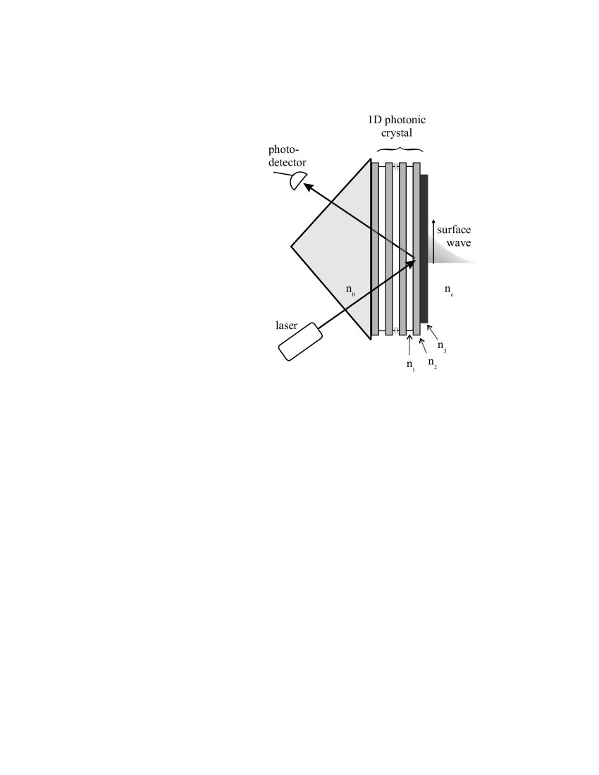
The one-dimensional photonic crystal (1-D PC) is a simple periodic multi-layer stack. Optical surface modes in 1-D PCs were studied in the 1970s, both theoretically Yeh et al. (1977) and experimentally Yeh et al. (1978). Twenty years later, the excitation of optical surface waves in a Kretschmann-like configuration was demonstrated Robertson and May (1999). A scheme of the Kretschmann-like excitation of PC SWs is presented in Fig. 1. In recent years, the PC SWs have been used in ever-widening applications in the field of optical sensors Konopsky and Alieva (2007); Shinn and Robertson (2005); Konopsky and Alieva (2009a, 2010, b); Konopsky et al. (2009). In contrast to SPPs, both p-polarized and s-polarized optical surface waves (with a dielectric final layer of the 1-D PC) Konopsky and Alieva (2007, 2009a, 2010) can be used in PC SW sensor applications. However, in applications in which the LRSPP propagates in a metal nanofilm deposited on an appropriate 1-D PC surface (e.g., in hydrogen detection Konopsky and Alieva (2009b); Konopsky et al. (2009)), only p-polarized waves can be used. Therefore, a unified theoretical description of PC SWs for both polarizations would be very useful, and such a description is presented in this article. Additionally, the current contribution describes conditions for the propagation of LRSPP in metal nanofilms (including lossy ones) that are deposited on the top of the 1-D PC structure and, thereby, provides the theoretical background for the works Konopsky and Alieva (2006, 2009b); Konopsky et al. (2009).
II Dispersion relation for s- and p-polarized surface waves in impedance terms
II.1 Impedance approach: basic definitions and recursion relation for a multilayer
The “characteristic impedance” of an optical medium is the ratio of the electric field amplitude to the magnetic field amplitude in this medium, i.e., . The concept of impedance in the optics of homogeneous layers is based on a mathematical analogy between a cascade of transmission line sections and a multilayer optical coating.
For reflection from a plane interface, the useful value is the “normal impedance” Brekhovskikh (1980); Delano and Pegis (1969) , which is the ratio of the tangential components of the electric field to the magnetic field:
| (1) |
Impedances for the s-polarized wave (in which the electric field vector is orthogonal to the incident plane — TE wave) and for the p-polarized wave (in which the electric field vector is parallel to the incident plane — TM wave) are correspondingly:
| (2) | |||||
| (3) |
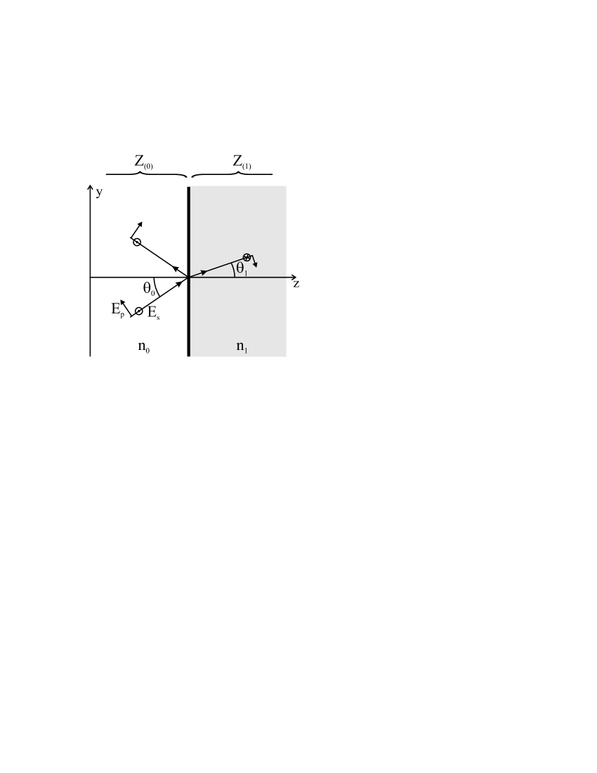
For the interface between semi-infinite media and (Figure 2), Fresnel’s formula for reflection coefficients has a very simple form in the impedance terms:
| (4) |
where is the normal impedance of medium , given by (2) or (3). Hereafter, the use of and (without subscripts or ) means that the equation holds for both polarizations when the corresponding impedances or are inserted. Fresnel’s formulas for transmission coefficients are as follows:
| (5) | |||||
| (6) |
In Figure 2, the labeling of the s-polarized wave in the first and the second media by and indicates the direction of the electric field vector after transmission/reflection in accordance with our “rule of signs.”
The equations for reflection coefficients of s- and p-polarized waves from any complex multilayer (see Figure 3) also have a form similar to equation (4):
| (7) |
where is an apparent input impedance for a multilayer, i.e., it is the impedance that is seen by an incoming wave as it approaches to the interface.
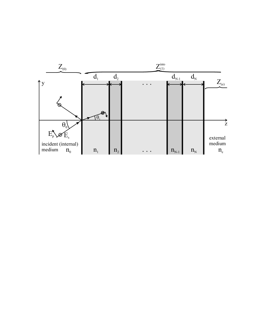
If the multilayer is made up of plane-parallel, homogeneous, isotropic dielectric layers (with refractive indices and geometrical thicknesses , where ) between semi-infinite incident (0) and external (e) media (see Fig(3)), the apparent input impedance of a semi-infinite external medium (e) and layers from to may be calculated by the following recursion relation Brekhovskikh (1980); Delano and Pegis (1969):
| (8) |
where ; and , while by definition.
Fresnel’s formulas for multilayer transmission coefficients are as follows:
| (9) | |||||
| and: | |||||
| (10) |
where are transmission coefficients at an interface between the layer and the layer.
II.2 The input impedance of a semi-infinite 1-D PC
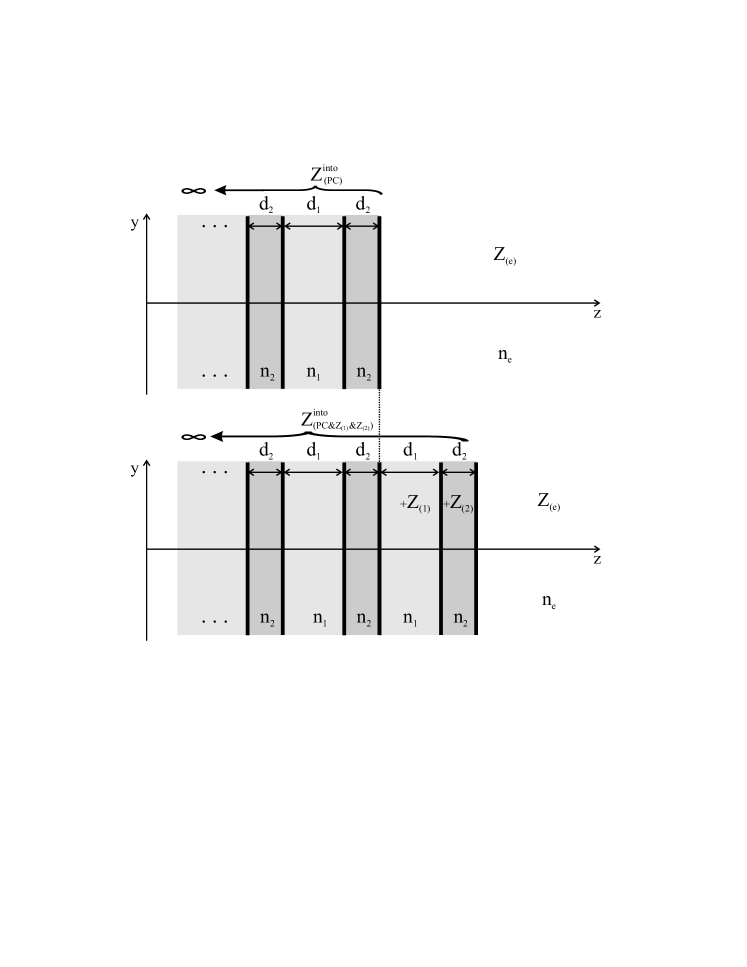
Now, we are ready to obtain the input impedance of the 1-D PC. Let us assume that we have a semi-infinite multilayer that consists of alternative layers with impedances and and its input impedance is unknown (see the top of Figure (4)). To find it, we make a next trick: first, we add an additional layer with impedance to the multilayer and find the input impedance of this system using the recursion relation (8):
| (11) |
Then, we add an additional layer with impedance to this system and obtain the same semi-infinite multilayer again (see the bottom of Figure (4)) with the input impedance:
| (12) |
It is obvious that , and, by solving equations (12) and (11) for , we obtain:
| (13) |
where .
II.3 Dispersion relation for surface waves
Now, we find the dispersion relation for surface waves in 1-D structures ended by an arbitrary layer with impedance . (It may be a layer with any , for example a metal layer). The input impedance of such a structure will be:
| (14) |
A general condition for the existence of a surface wave between two media with impedances and is:
| (15) |
In our case, this condition takes the form:
| (16) |
By solving equations (16) and (14), we obtain the dispersion relation for the optical surface waves in the 1-D PC:
| (17) |
where is a whole number.
This is a general dispersion relation, which is valid for both polarizations. If one would like to obtain the dispersion of the s-polarized optical surface wave, one should use the impedances in (17) and (13). Accordingly, to obtain the dispersion of the p-polarized optical surface wave, one must use impedances in (17) and (13).
It should be noted that the solution obtained for s-polarization is equivalent (at ) to the solution derived from a dispersion relation for an s-polarized optical surface wave, which was deduced by Yeh, Yariv and Hong using the unit cell matrix method (see equation (58) in Ref. Yeh et al. (1977)). Meanwhile, the solution for p-polarization is equivalent to the solution derived from the dispersion relation for a p-polarized optical surface wave, which we deduced in a similar manner (using the unit cell matrix method) in Ref. Konopsky and Alieva (2006) (see equation (2) in Ref. Konopsky and Alieva (2006)). The dispersion relation (17) and the relations presented in Refs. Yeh et al. (1977); Konopsky and Alieva (2006) were derived by different approaches (but, of course, both started from the same Maxwell equations and boundary conditions) and presented in different terms, but these relations give the same results and may be transformed to each other. The advantages of the presented dispersion relation with the impedance terms are its compact structure and its unified form for both polarizations. In addition, a visible physical interpretation the impedance terms in the current dispersion relation allows it to be easily extended for use with more complicated structures. For example, the addition of an adsorption layer between the layer (3) and the external medium (e) may be taken into account simply by changing of the impedance by the impedance calculated via recursion relation (8), where impedance of the external medium is convoluted with an impedance of the adsorption layer .
II.4 Band gap maximum extinction per length
As a rule, in practical applications, we have values of two RIs of alternative media in the 1-D PC, and the purpose is to find the thicknesses of each alternative layer, which provides the maximum extinction per length at given RIs, wavelength and angle. Below, we derive this condition for the maximum extinction, which makes it possible to minimize overall thickness of 1-D PC. Also, we show that the commonly-held opinion that it is a “quarter-wave-length” thickness of the layers that provide the maximum extinction per length is incorrect.
To find the condition for the maximum extinction we derive the transmission coefficient for one period of the PC (two layers), that is, the transmission through the three interfaces:
| (18) |
where expressions for are given by equations (9) or (10). As a result we obtain for both polarizations:
The desired values of the thicknesses and are the thicknesses at which the next expression:
| (20) |
reaches its maximum. Absolute values are inserted in equation (20) in order to obtain the same result regardless of the sign in equation (13). It may be noted that the “quarter-wave-length” thicknesses of the layers, , are values that maximize another expression, namely, expression (20) without the denominator, i.e., and these “quarter-wave-length” thicknesses are not optimal, especially at large incident (grazing) angles (i.e. at ).
Now, we have all the equations required to calculate a 1-D PC structure for any particular experimental conditions. Presented below is an example in which we obtain the 1-D PC structure ended by a Pd nanolayer, which were successfully used for hydrogen detection in Refs. Konopsky and Alieva (2009b), Konopsky et al. (2009).
III Calculation of the 1-D PC structure for particular experimental conditions
III.1 Angle-dependent variables
It is very convenient to use a numerical aperture as an angle variable instead of angles in each -th layer and hereafter we will do so. It is a unified angle variable for all layers, since according to Snell’s law , for any . The angle-dependent variables have the next forms as functions of :
| (21) | |||||
| (22) | |||||
| (23) |
III.2 Conditions for long-range propagation of the plasmon-polariton waves in metal films
A value of at which we would like to excite a PC SW (and, therefore, a desired SW wavevector depends on the particular problem that we are trying to solve. As one example, to excite LRSPPs in thin metal films, the effective RI of the LRSPPs should be close to the RI of the external medium . To prove this statement, in this subsection we will find the angular value at which the electric field of the incident p-polarized wave has a minimum inside a thin layer with a large extinction for optical waves. This minimum coincides with the zero of the main, tangential component of the electric field in the film with the large extinction. This large extinction, i.e., large imaginary part of the RI of a thin film material (), may arise both from a large negative permittivity of the material (, even at small , as is the case for silver or gold) and from a large losses in the material (, even at small or positive , as is the case for palladium). In both cases the optical wave does not penetrate deeply in the bulk material with permittivity . It should be also noted that, in a very thin film, additional losses always appear due to collision-induced scattering of conducting electrons at the walls of the film. Therefore, the imaginary part of the permittivity in such a film is increased in comparison with the bulk material (see Appendix B for details).
So, let us assume that we have a thin film with RI and that a p-polarized light wave is incident on it with angular parameter . The instantaneous value of the tangential component of the electric field at a coordinate point inside the film is the sum of the progressive and the recessive (reflected) waves:
| (24) | |||||
where the reflection coefficient from the interface between the film (3) and the external medium (e) is given by (7):
| (25) |
To find the coordinate at which the tangential component of the electric field in the film is zero, we solve the equation:
| (26) |
with respect to . Then we express the coordinate as , where is the coordinate of the zero minimum in terms of film thickness . When (), the zero of the takes place at an internal border of the film. When (), the field zero occurs in the center of the film. When (), the field zero is located at an external border of the film. The solution of equations (26, 24) is:
| (27) |
Assuming that we will use the impedance of the final (metal) film in the so-called Leontovich approximation (see, for example, Ref. Senior (1960) for details). In this approximation equations (22) and (23) have the form:
| (28) | |||||
| (29) |
while
| (30) |
as usual.
Substituting (28), (29) and (30) in (25) and in equation (27) and then solving it for we get (in the approximation ):
| (31) |
which we presented earlier (see eq. (1) in Ref. Konopsky and Alieva (2006)).
So, we have derived equation (31), which shows that the modulus of the electric field strength has a minimum equal to zero when the p-polarized electromagnetic wave incident on the thin (metal) film in the angular range from to . In this case, the point at which is changed from the internal () to the external () borders of the film, and it is located in the center of the film at ().
Now the next question arises: are there some electromagnetic surface modes with a wavevector in the range: ? If the answer is yes, one may expect that these modes will be long-range propagated surface modes, since they may be excited by the p-polarized waves incident on the film in the angular range , and these modes have the zero minimum of inside the lossy (metal) film.
One example of such a mode is widely recognized – it is the LRSPP in a thin film embedded between two identical dielectrics. It is known that the dispersion curve of SPPs splits as a result of a coupling between SPPs from both film interfaces, and the LRSPP wavevector shifts (at a given frequency) to a light curve (i.e., ). The value of the LRSPP wavevector is (see Ref. Yang et al. (1991) and/or Appendix A), where is given by (31) at , and the zero minimum of is always located in the center of the film.
PC SWs are another example of electromagnetic surface modes that can propagate along thin metal films and have a wavevector in the range of . In the next subsection we show how to design the PC structure for excitation PC SW at desired at given , and .
III.3 Derivation of , and for PC structure terminated by Pd nanofilm
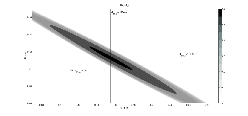
So, let us to design PC structure with a maximum band gap extinction at desired (obtained from (31) at , nm and nm). Let us have two layer materials, and , with RIs of and at the wavelength of our tunable diode laser (at nm). The function given by (20) is presented in Fig. 5. One can see that reaches its maximum at nm and nm. At these thicknesses, the maximum band gap extinction per length occurs, and, therefore, the PC structure will have a minimal overall thickness.
Now, we must find the thickness of the final palladium layer that will satisfy the dispersion relation (17). With we have:
| (32) |
Substituting and the other values pointed in the present subsection into (32) (and into (22), (23) and (13) correspondingly) we obtain nm. This is a rather small value and it is better for the thickness of the palladium layer to be in the range of nm to be sure that a continuous film we will obtain during deposition. If we want to retain the maximum band gap extinction at the desired and, therefore, do not want to change the optimal values and , we may decrease the thickness of just the layer, which is contiguous with the layer. The decrease in the thickness of the last layer from nm to nm permits us to increase the thickness of the layer to the value nm and satisfy the SW excitation condition at the desired angle and the desired wavelength .
Thus we derive the next PC structure: substrate//air, in which is a layer with a thickness nm, is a layer with nm, is a layer with nm, and is the palladium layer with nm. In Fig. 6 the calculated dispersion of this 1-D PC structure in air is presented as the logarithm of the optical field enhancement (i.e., as ) in the external medium near the structure. The optical field enhancement is calculated by using (10) and (8) for 29 dielectric layers and one metal nanolayer on BK-7 () substrate. The optimal number of pairs depends on a total extinction in the layers. In the present case, the nanolayer is the layer that gives the main contribution in extinction and the 14 pairs provide the optimal coupling (i.e., ) of the incoming EM radiation into SWs.
The dispersion is presented using the coordinate . The angular parameter , at which the excitation of the surface mode occurs, is equal to the effective RI of the mode, . Therefore, the red curve that is inside the blue band gap in Fig. 6 presents the dispersion of the LRSPP mode (i.e., the dependence of its effective RI on the wavelength).
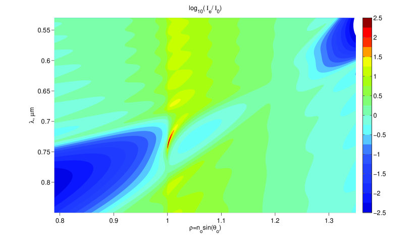
One can see from Fig. 6 that in accordance with (31) the LRSPP mode exists near only (), where the minimum of EM field inside the metal nanolayer occurs, while, at the EM damping is increased significantly in this 8-nm thick metal film.
In the presented case the optical surface mode dispersion curve approaches the line of the total internal reflection (TIR) () at wavelengths in the range of nm. Therefore, at these wavelengths, we can excite the SPP at and expect it to be LRSPP. At nm (), the zero minimum of occurs at the internal interface of the 8 nm palladium film, while at nm () the zero minimum of occurs in the center of this 8-nm thick nanofilm. Moreover, at nm (, i.e., ) we can excite LRSPP with near the external interface of the film, and this wave will have the largest propagation length. Theoretical propagation lengths, i.e., propagation lengths that take into account the internal damping in the Pd nanofilm but do not take into account the surface scattering of LRSPPs to photons, for these wavelengths are: mm, mm and mm. Therefore, contrary to intuitive expectations, modes with ( at the external interface of the film, i.e., modes with an asymmetric field distribution in the nanofilm) are more long-range propagated than the mode with ( in the center of the film). More details about this issue are provided in Appendix A.
IV Conclusions
The present article provides the theoretical background and the algorithm for the design of 1-D PC structures that support the propagation of optical surface waves. We have used the impedance approach, which permits calculation for s- and p-polarizations by the same equations. The main results of this work are the input impedance of semi-infinite 1-D PC (13) and the dispersion relation of PC SWs (17). Equations (19) and (20) are needed for the design of a multilayer structure with maximal band gap extinction at the minimal overall thickness of the structure. Equation (31) is important for understanding of the physical reasons for the propagation of the LRSPP even in thin films with large extinction, while the equations in Appendix A provide additional insight concerning why slightly asymmetrical structures provide more long-range propagation of the surface waves.
Acknowledgments
This work was supported financially by the Russian Federal Program “Research and educational personnel of innovative Russia” and by the Russian Foundation for Fundamental Research. The author thanks E.V. Alieva for useful discussions and assistance.
Appendix A: Dispersion relation for LRSPPs in the symmetrical configuration and increase of propagation length associated with slight asymmetry in the system.
The propagation of LRSPP in a symmetrical structure (metal film between identical dielectrics) has been considered in several publications Sarid (1981); Yang et al. (1991). Here we will consider this point based on the impedance approach and then will add slight asymmetry to the structure.
The dispersion relation, , for surface waves in a metal film between two semi-infinite dielectric media can be obtained easily, for example, from equation (17) or equation (32), in which the 1-D PC is replaced by a uniform dielectric medium with a RI ():
| (A1) |
For a pure symmetrical configuration [ and ], the general dispersion relation (A1) has the form shown below:
| (A2) |
By taking into account the Leontovich approximation, (28) and (29), the equation can be simplified further:
| (A3) |
For a very thin film (at ) one can obtain two solutions for from (A3):
| (A4) | |||||
| (A5) |
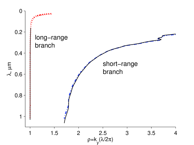
The former equation presents an approximation for the long-range branch of the dispersion relation of a symmetrical system (A2), while the latter is an approximation for the short-range branch (its damping increases at ). In Fig. 7, graphical illustrations of dispersion relation (A2) [or (A3), since no difference can be seen between them at this scale] and its approximations (A4) and (A5) are presented. Calculations are performed for an 8-nm thick Pd film that is suspended freely in the air (), and the Pd RIs at different wavelengths were taken from Ref. Palik (1985). In addition to good agreement between the dispersion equation for the symmetrical system and the approximated equations, (A4) and (A5), Fig. 7 shows that the long-range branch of the curve has no noticeable wavelength dispersion in the visible range, while the system with PC from one side the LRSPP curve (see Fig. 6) has prominent dispersion.
It is apparent that (A4) consides exactly with (31) at , and, therefore, in a pure symmetrical configuration, the zero of the tangential component and the total minimum of the electric field are always located in the center of the metal nanofilm, which is not surprising due to the symmetry of the system. A more surprising fact is that this symmetrical system (with in the center of the film) is not the optimal solution if one is looking for the smallest damping and the longest propagation length of the LRSPP. To the best of our knowledge Wendler and Haupt were the first to point out on this peculiarity. In the theoretical article Wendler and Haupt (1986) they showed, through numerical calculations, that, in a slightly asymmetrical structure, the propagation length may be three orders of magnitude greater than the propagation length in the symmetrical structure.
In experimental practice Konopsky and Alieva (2006), Konopsky and Alieva (2009b) we have been able to increase the propagation length of SPPs by a factor in the range of 100-200 times. Further increase is limited by damping due to surface scattering, which occurs due to the close proximity of the effective RI of the LRSPP to the RI of the external medium, or, in other words, “the plasmon curve becomes too close to the light line”. Therefore, any small disturbance can transform plasmons to photons when this zero minimum is approaching the border of the film (and, therefore, ). But, nevertheless, the internal damping of LRSPPs can be decreased when slight asymmetry exists in the structure.
Below, we obtain analytical expressions for the optimal difference between the RIs of the dielectrics and show that the propagation length of the LRSPP increases when the minimum of the electric field shifts to the interface of the film (but does not leave the borders of the film). To do this, we return to the general dispersion relation for a non-symmetrical system (A1) and assume that the RIs of the dielectrics on both sides of the metal film differ only by a small value :
| (A6) |
We are solving for the LRSPP wave only, so will differ from by a small value :
| (A7) |
where – see (A4).
In the limit, with small and small , the dispersion relation (A1) can be simplified to the form:
| (A8) |
Solving this equation for and taking its imaginary part we obtain the next extinction of LRSPPs in a slightly asymmetrical system:
| (A9) |
This over-approximated imaginary part of the effective RI of the LRSPP has two solutions with (approximately) zero extinction, , and, therefore, with maximal propagation length, namely, the first solution is and the second solution is:
| (A10) |
which in the limit is:
| (A11) |
One can see that (A11) coincides with the addition to from (31) at (i.e., when the minimum of the field is at the nanofilm border). Therefore, expression (A10) also may be considered as a cutoff condition for the existence of LRSPPs (at no bounded modes exist). From (A1), it can be determined that, at , the effective RI of LRSPP is infinitesimally close to the TIR angle, i.e., .
It is worth noting here that the analytical expression for from (A10) corresponds well with numerical data presented by Wendler and Haupt in Ref. Wendler and Haupt (1986). Even the over-approximated expression for from (A11), which is not dependent on the nanofilm RI , is coincident with these numerical data at small film thicknesses (i.e., nm).
At excitation of ultra-long-range SPP in thin films by introducing a small asymmetry in the system and, therefore, by abutting the plasmon curve on the light line, it is very important to maintain an appropriative balance between decreasing the internal damping of LRSPPs and increasing the scattering of the LRSPPs. The possibility for tuning system parameters during the experiment to find the optimum is extremely convenient in this case.
The principal difference between D/M/D’ and D/M/PC systems is that, in the system with a 1-D PC on one side, it is experimentally easy to introduce such a small asymmetry (in effective RI) by tuning the wavelength of the laser, while it is really difficult to (finely) tune the dielectric constants on the one interface by any means. Wavelength tuning would be not useful in the D/M/D’ case, because dispersion of dielectrics is small in non-absorbing wavelength regions, while wavelength tuning in the PC structure is very effective due to the high wavelength dispersion inside the band gap regions.
Appendix B: Additional damping in thin film.
Damping of EM waves in thin metal films increases due to collision-induced scattering of conducting electrons at the walls of the film. This occurs when the mean free path of the electrons becomes comparable to the characteristic dimensions of the system. Therefore, the imaginary part of the permittivity in such a film is increased in comparison with the bulk material. Unfortunately in many articles (especially theoretical articles), authors have usually disregarded this fact and used overly optimistic values for the imaginary part of the metal permittivity.
Here we present a summary of formulae for this case, which help to estimate the minimal addition to . At optical frequencies, the damping in nanostructures with the characteristic dimension is
| (B1) |
where is the damping constant for the bulk sample and is the electron velocity on the Fermy surface. Below, several specific cases are considered.
IV.0.1 Nanofilm as a set of nanoparticles:
For sphere Bohren and Huffman (1983)
| (B2) |
where is plasma frequency. Therefore, the characteristic dimension in this case is ( is the radius of the sphere).
IV.0.2 Continuous film:
For continuous film with thickness Thèye (1983):
| (B3) |
For very thin film (nanofilm), in the limit
| (B4) |
(therefore in this limit) and
| (B5) |
while in the general case
| (B6) |
We have considered only collision-induced damping, and we did not take into account other types of damping in small volumes, which may lead to further increases of the imaginary part of the nanosized materials at optical frequencies.
The collision-induced damping increase in the nanofilm at zero frequency may be estimated by Fuchs’ formula Larson (1971) for a specific electrical resistance of continuous films. For example, in our work with gold nanofilm Konopsky and Alieva (2006), the electrical resistance of the nanofilm was 850 for a strip that was with 0.25 mm wide and 6.5 mm long. Therefore, for our nanofilm thickness of 5 nm, the specific resistance in the nanofilm was cm, which is 7.4 times greater than the specific resistance of bulk gold (cm). While according to Fuchs formula at Larson (1971)
| (B7) |
Substituting the mean free path of electrons in bulk gold, which at room temperature is nm, we obtain that the specific resistance of the 5 nm gold film at room temperature should be about six times greater than that of bulk gold. This value is in good agreement with the measured value, taking into account imperfections of the sputtered gold nanofilm.
References
- Raether (1988) H. Raether, Surface Plasmons (Springer, Berlin, 1988).
- Liedberg et al. (1983) B. Liedberg, C. Nylander, and I. Lundström, Sensors and Actuators 4, 299 (1983).
- Sarid (1981) D. Sarid, Phys. Rev. Lett. 47, 1927 (1981).
- Craig et al. (1983) A. E. Craig, G. A. Olson, and D. Sarid, Opt. Lett. 8, 380 (1983).
- Yang et al. (1991) F. Yang, J. R. Sambles, and G. W. Bradberry, Phys. Rev. B 44, 5855 (1991).
- Konopsky and Alieva (2006) V. N. Konopsky and E. V. Alieva, Phys. Rev. Lett. 97, 253904 (2006).
- Yablonovitch (1993) E. Yablonovitch, J. Opt. Soc. Am. B 10, 283 (1993).
- Kossel (1966) D. Kossel, J. Opt. Soc. Am. 56, 1434 (1966).
- Yeh et al. (1977) P. Yeh, A. Yariv, and C.-S. Hong, J. Opt. Soc. Am. 67, 423 (1977).
- Yeh et al. (1978) P. Yeh, A. Yariv, and A. Y. Cho, Appl. Phys. Lett. 32, 104 (1978).
- Robertson and May (1999) W. M. Robertson and M. S. May, Appl. Phys. Lett. 74, 1800 (1999).
- Konopsky and Alieva (2007) V. N. Konopsky and E. V. Alieva, Anal. Chem. 79, 4729 (2007).
- Shinn and Robertson (2005) A. Shinn and W. Robertson, Sens. Actuator B-Chem. 105, 360 (2005).
- Konopsky and Alieva (2009a) V. N. Konopsky and E. V. Alieva, in Biosensors and Biodetection, Methods and Protocols, Volume 1: Optical-Based Detectors, edited by A. Rasooly and K. E. Herold (Humana Press, Totowa, NJ, USA, 2009a), vol. 503 of Springer Protocols: Methods in Molecular Biology, chap. 4, pp. 49–64.
- Konopsky and Alieva (2010) V. N. Konopsky and E. V. Alieva, Biosens. Bioelectron. 25, 1212 (2010).
- Konopsky and Alieva (2009b) V. N. Konopsky and E. V. Alieva, Opt. Lett. 34, 479 (2009b).
- Konopsky et al. (2009) V. N. Konopsky, D. V. Basmanov, E. V. Alieva, D. I. Dolgy, E. D. Olshansky, S. K. Sekatskii, and G. Dietler, New J. Phys. 11, 063049 (2009).
- Brekhovskikh (1980) L. Brekhovskikh, Waves in Layered Media (Academic, New-York, 1980).
- Delano and Pegis (1969) E. Delano and R. Pegis, in Progress in Optics, edited by E. Wolf (North-Holland, Amsterdam, 1969), vol. VII, chap. 2, pp. 67–137 (see pp.77, 130).
- Senior (1960) T. Senior, Appl. Sci. Res. Sec.B. 8, 418 (1960).
- Palik (1985) E. D. Palik, Handbook of Optical Constants of Solids (Academic, London, 1985).
- Wendler and Haupt (1986) L. Wendler and R. Haupt, J. Appl. Phys. 59, 3289 (1986).
- Bohren and Huffman (1983) C. Bohren and D. Huffman, Absorption and Scattering of Light by Small Particles (Wiley & Sons, New-York, 1983).
- Thèye (1983) M. Thèye, Phys. Rev. B 2, 3060 (1983).
- Larson (1971) D. C. Larson, in Physics of Thin Films, edited by M. H. Francombe and R. W. Hoffman (Academic, London, 1971), vol. VI, chap. 2.