Imaging Localized States in Graphene Nanostructures
Abstract
Probing techniques with spatial resolution have the potential to lead to a better understanding of the microscopic physical processes and to novel routes for manipulating nanostructures. We present scanning-gate images of a graphene quantum dot which is coupled to source and drain via two constrictions. We image and locate conductance resonances of the quantum dot in the Coulomb-blockade regime as well as resonances of localized states in the constrictions in real space.
keywords:
graphene, scanning-probe microscopy, quantum dots, nanoribbons+41 (0)44 63 33792 ETH Zurich]Solid State Physics Laboratory, 8093 Zurich, Switzerland ETH Zurich]Solid State Physics Laboratory, 8093 Zurich, Switzerland \alsoaffiliation[RWTH Aachen]JARA-FIT and II. Institute of Physics, 52074 Aachen, Germany ETH Zurich]Solid State Physics Laboratory, 8093 Zurich, Switzerland
Graphene has sparked intense research among theorists and experimentalists 1, 2 alike since its first successful fabrication in 2004 3. This is mainly due to graphene’s extraordinary band structure, a linear relationship between energy and momentum without a band gap. The gapless band structure, however, prohibits confining charge carriers by using electrostatic gates. Hence, lateral confinement in graphene relies on etched structures and the appearance of a transport gap in graphene constrictions 4, 5, 6. Nevertheless, already the first experiment on graphene nanoribbons by Han et al. 7 showed a discrepancy between the measured transport gap and a simple confinement-induced band gap. Theoretical models explain the observed gap by Coulomb blockade, edge scattering, and/or Anderson-type localization due to edge disorder 8, 9, 10, 11. On the experimental side, there is increasing evidence for Coulomb-blockade effects in nanoribbons 6, 12, 13, 14, 15.
Transport through graphene quantum dots in the Coulomb blockade regime is typically modulated by resonances arising from the constrictions 16. However, for both, nanoribbons and quantum dots, the microscopic origin of the transport gap and the resonances in the constrictions needs to be understood in more detail.
Hence, probing techniques which are capable of locally investigating properties of graphene nanostructures are essential. Earlier experiments of this kind on graphene include experiments with a scanning single-electron transistor 17, 18, scanning-tunneling spectroscopy 19, 20, 21, and scanning-gate microscopy 22, 23. All these experiments were performed on large area graphene sheets. Here, we present results of scanning-gate experiments on a single-layer graphene quantum dot which is coupled to source and drain leads via two constrictions. We observe ring-like resonances in the scanning-gate experiments centered at the quantum dot as well as in the constrictions. This enables us to map resonances in real space.
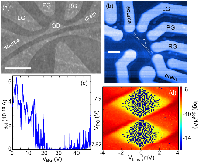
Atomic-force micrographs of the sample after etching under ambient conditions (a) and of the completed device at (b) are shown in Fig. 1. If not stated otherwise, the temperature of all measurements shown in this paper is . Fabrication details are given in the supporting information 24. We first show a backgate sweep in Fig. 1(c) with voltage applied between source and drain. The current through the dot is suppressed in the transport gap ranging approximately from to . The charge neutrality point is at , presumably because of charged impurities on or near the graphene surfaces. The charge stability diagram of the quantum dot in Fig. 1(d) was measured at the base temperature of the dilution refrigerator. We extract a charging energy which is comparable to the values found in other devices of similar size 5.
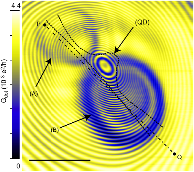
We performed scanning-gate measurements of the quantum dot in the hole regime at (see supporting information 24 and Ref. 25 for further information on our scanning-gate setup). To this end, the conductance of the quantum dot is recorded as the voltage-biased tip is scanned at constant height above the structure 26, 27, 28. A representative result is shown in Fig. 2; further images in the same regime are presented in the supporting information 24. The scan frame has an area of and the outline of the quantum dot, as obtained from topographical images (see Fig. 1(b)), is shown with dashed, black lines. We observe three sets of concentric rings which are marked by arrows labelled (QD), (A), and (B). The set (QD) is caused by Coulomb resonances of the quantum dot as verified by the presence of Coulomb-blockade diamonds when sweeping the tip and bias voltages (not shown here) and we refer to them as Coulomb rings. The conductance does not drop to zero between two Coulomb rings because the measurements were done at the edge of the transport gap in backgate voltage where the coupling of dot states to source and drain is rather strong.
Most strikingly, we observe two additional sets of rings (A) and (B). In the following, we will refer to them as resonances A and B, respectively. In all scanning-gate images taken on this sample, resonances A and B are manifest as amplitude-modulations of the Coulomb resonances of the quantum dot. They are centered around points in the constrictions connecting the quantum dot to source and drain. Their presence allows to locate regions of localized charge carriers in the constrictions. This is a central result of this paper. The interpretation of rings A and B as being due to localized states will be corroborated below. Only one or at maximum two localized states are observed in each constriction.
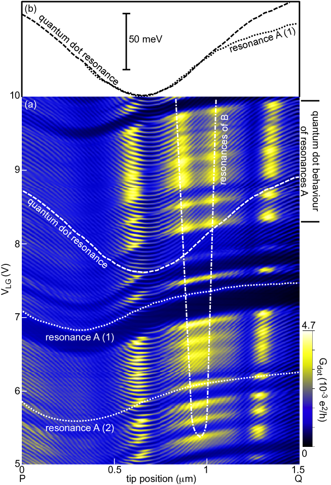
In electronic transport, resonances are in general localized in space and sharp in energy. In order to confirm this for resonances A and B, we took linescans between points P and Q in Fig. 2 and changed the energy of the localized states by stepping the left side gate voltage from up to . The result is shown in Fig. 3(a). We can identify quantum dot resonances (dashed, white line and resonances parallel to it), resonances A (dotted, white lines and resonances parallel to them), and resonances B (dash-dotted line and resonance parallel to it).
The tip-induced potential at any fixed location in the graphene plane is changed when moving the tip from P to Q. We stay on a particular resonance by compensating for this change at the location of the resonance with . This leads to the characteristic slopes of resonances A and B and the quantum dot resonances. The left side gate is closest to the center of resonance A; resonance B is furthest away. Therefore resonances A are strongly tuned by the left gate, whereas resonances B are only slightly affected. Quantum dot resonances are in between. Below we will use this effect to deduce the lever arm ratio of the lever arms of the left gate on the dot, , and on resonance A, .
Horizontal cuts in Fig. 3(a), i. e. cuts for fixed , show that all resonances eventually shrink to a single point in space. This allows us to identify them with states localized in space at this point. Vertical cuts, on the other hand, show that they are reasonably sharp in energy. However, we notice a strong variation in the width of the resonances; e. g. resonance A(2) is much sharper than resonance A(1). A closer inspection of the sharper resonances of A reveals that they are accompanied with avoided crossings of the quantum dot Coulomb resonances.
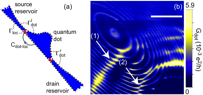
We propose the model shown in Fig. 4(a) which is capable of capturing the essential details of our observations. It consists of a quantum dot coupled to source and drain via two tunnel barriers with tunnel coupling . We introduce an additional localized state located in the constriction and coupled to the lead via a tunnel barrier with coupling . The localized state interacts with the quantum dot states by tunneling through the barrier and by mutual capacitive coupling via .
Fig. 4(b) shows a scanning-gate image taken at the temperature . Coulomb resonances are now much sharper than in Fig. 2 and Fig. 3(a). Resonances B lead to a modulation of the dot conductance as highlighted by arrows (1) and (2). The capacitive coupling between resonance B and the quantum dot leads to the avoided crossings pointed at by arrow (2). They are more easily identified compared to Fig. 3(a) because of the lower temperature (see supporting information for a further scanning-gate image in this regime 24).
Whenever such an avoided crossing occurs, resonance A or B is charged with an additional charge carrier. Thus resonances originate from localized states. The capacitive coupling shifts the chemical potential in the dot when the localized state is charged. Consequently, the Coulomb ring in the scanning-gate image is shifted as well. Charging effects are not observed for all crossings of quantum dot resonances with resonances A or B. Avoided crossings of Coulomb resonances occur only for narrow resonances A and B; the broader ones do not show the signature of charge quantization as inspection of Fig. 3 and Fig. 4 show. The tunnel coupling strength must therefore depend strongly on the Fermi energy. Then charging of a localized state with discrete charges occurs only if is below a certain threshold such that the condition for the conductance of the localized state is fulfilled. The width of the resonance is also determined by the tunnel coupling if .
Whenever a localized state shows quantum dot-like behavior, we can infer its size from its charging energy. In order to do so, we pick just those resonances of A in Fig. 3 which show avoided crossings with quantum dot resonances. We identify six resonances of this type in the regime denoted by “quantum dot behavior of resonances A”. They have a spacing of in left-gate voltage. In order to convert this voltage scale to an energy, we need to know the lever arm of the left gate onto the localized state. Coulomb resonances of the quantum dot are separated on average by in left-gate voltage. Combined with the charging energy , this yields a lever arm of . The two dotted lines in Fig. 3(a) denote how resonances of A evolve as a function of position. If we scale these lines by a factor of 1.67 in -direction and shift them along the x-axis (the “position”) such that their minima coincide with a minimum of a Coulomb resonance, they nicely fit onto each other over a range of almost as shown in Fig. 3(b). (For tip positions , screening effects lead to a different progression of the quantum dot resonance and the resonances of localized state A.) This gives us the possibility to estimate the desired lever arm . It is given by . Consequently the charging energy of the localized state A is between and . This corresponds to a radius of the localized state of assuming with and lithographic size of the dot . Previous experiments obtained similar sizes by means of conventional transport experiments for graphene nanoribbons 12, 13, 31. However our method allows to determine relative lever arms of localized states in more complex structures such as the presented quantum dot device.
Stampfer et al. report on a variation of relative lever arms of localized states in nanoribbons by up to 30% 14. This is explained with a number of localized states spread along the nanoribbon. Based on the geometry of the device used in 14, a rough estimate yields a spread of over 300 nm. With our scanning-gate microscope, a spread of more than 100 nm should easily be detectable. The fact that we observe one localized state per constriction is most likely due to the short length of the constrictions.
Financial support by ETH Zürich and the Swiss National Science Foundation is gratefully acknowledged. Some images have been prepared using the WSxM-software 32.
The supporting information includes description on the sample preparation and of our scanning-gate setup. Additionally more scanning-gate images are shown to corroborate some statements of this letter.
References
- 1 Geim, A. K.; Novoselov, K. S. Nat. Mater. 2007, 6, 183.
- 2 Castro Neto, A. H.; Guinea, F.; Peres, N. M. R.; Novoselov, K. S.; Geim, A. K. Rev. Mod. Phys. 2009, 81, 109.
- 3 Novoselov, K. S.; Geim, A. K.; Morozov, S. V.; Jiang, D.; Katsnelson, M. I.; Dubonos, S. V.; Grigorieva, I. V.; Firsov, A. A. Science 2004, 306, 666.
- 4 Ponomarenko, L. A.; Schedin, F.; Katsnelson, M. I.; Yang, R.; Hill, E. W.; Novoselov, K. S.; Geim, A. K. Science 2008, 320, 356.
- 5 Stampfer, C.; Güttinger, J.; Molitor, F.; Graf, D.; Ihn, T.; Ensslin, K. Appl. Phys. Lett. 2008, 92, 012102.
- 6 Liu, X.; Oostinga, J. B.; Morpurgo, A. F.; Vandersypen, L. M. K. Phys. Rev. B 2009, 80, 121407(R).
- 7 Han, M. Y.; Özyilmay, B.; Zhang, Y.; Kim, P. Phys. Rev. Lett. 2007, 98, 206805.
- 8 Sols, F.; Guinea, F.; Castro Neto, A. H. Phys. Rev. Lett. 2007, 99, 166803.
- 9 Mucciolo, E. R.; Castro Neto, A. H.; Lewenkopf, C. H. Phys. Rev. B 2009, 79, 075407.
- 10 Evaldsson, M.; Zozoulenko, I. V.; Xu, H.; Heinzel, T. Phys. Rev. B 2008, 78, 161407(R).
- 11 Schubert, G.; Schleede, J.; Fehske, H. Phys. Rev. B 2009, 79, 235116.
- 12 Todd, K.; Chou, H.-T.; Amasha, S.; Goldhaber-Gordon, D. Nano Lett. 2008, 9, 416.
- 13 Molitor, F.; Jacobsen, A.; Stampfer, C.; Güttinger, J.; Ihn, T.; Ensslin, K. Phys. Rev. B 2009, 79, 075426.
- 14 Stampfer, C.; Güttinger, J.; Hellmüller, S.; Molitor, F.; Ensslin, K.; Ihn, T. Phys. Rev. Lett. 2009, 102, 056403.
- 15 Gallagher, P.; Todd, K.; Goldhaber-Gordon, D. Phys. Rev. B 2010, 81, 115409.
- 16 Stampfer, C.; Schurtenberger, E.; Molitor, F.; Güttinger, J.; Ihn, T.; Ensslin, K. Nano Lett. 2008, 8, 2378.
- 17 Martin, J.; Akermann, N.; Ulbricht, G.; Lohmann, T.; Smet, J. H.; von Klitzing, K.; Yacoby, A. Nat. Phys. 2008, 4, 144.
- 18 Martin, J.; Akermann, N.; Ulbricht, G.; Lohmann, T.; von Klitzing, K.; Smet, J. H.; Yacoby, A. Nat. Phys. 2009, 5, 669.
- 19 Zhang, Y.; Brar, V. W.; Wang, F.; Girit, C.; Yayon, Y.; Panlasigui, M.; Zettl, A.; Crommie, M. F. Nat. Phys. 2008, 4, 627.
- 20 Zhang, Y.; Brar, V. W.; Girit, C.; Zettl, A.; Crommie, M. F. Nat. Phys. 2009, 5, 722.
- 21 Li, G.; Luican, A.; Andrei, E. Y. Phys. Rev. Lett. 2009, 102, 176804.
- 22 Berezovsky, J.; Westervelt, R. M. arXiv:0907.0428 2010.
- 23 Connolly, M. R.; Chiou, K. L.; Smith, C. G.; Anderson, D.; Jones, G. A. C.; Lombardo, A.; Fasoli, A.; Ferrari, A. C. arXiv:0911.3832 2009.
- 24 see Supporting Information
- 25 Gildemeister, A. E.; Ihn, T.; Barengo, C.; Studerus, P.; Ensslin, K. Rev. Sci. Instrum. 2007, 78, 013704.
- 26 Topinka, M. A.; LeRoy, B. J.; Westervelt, R. M.; Shaw, S. E. J.; Fleischmann, R.; Heller, E. J.; Maranowski, K. D.; Gossard, A. C. Nature 2001, 410, 183.
- 27 Pioda, A.; Kicin, S.; Ihn, T.; Sigrist, M.; Fuhrer, A.; Ensslin, K.; Weichselbaum, A.; Ulloa, S. E.; Reinwald, M.; Wegscheider, W. Phys. Rev. Lett. 2004, 93, 216801.
- 28 Gildemeister, A. E.; Ihn, T.; Sigrist, M.; Ensslin, K.; Driscoll, D. C.; Gossard, A. C. Phys. Rev. B 2007 75, 195338.
- 29 Schnez, S.; Molitor, F.; Stampfer, C.; Güttinger, J.; Shorubalko, I.; Ihn, T.; Ensslin, K. Appl. Phys. Lett. 2009, 94, 012107.
- 30 Gildemeister, A. E.; Ihn, T.; Sigrist, M.; Ensslin, K.; Driscoll, D. C.; Gossard, A. C. Appl. Phys. Lett. 2007, 90, 213113.
- 31 Han, M. Y.; Brant, J. C.; Kim, P. Phys. Rev. Lett. 2010, 104, 056801.
- 32 Horcas, I.; Fernandez, R.; Gomez-Rodriguez, J. M.; Colchero, J.; Gomez-Herrero, J.; Baro, A. M. Rev. Sci. Instrum. 2007, 78, 013705.
![[Uncaptioned image]](/html/1005.2024/assets/x5.png)