Vortex manipulation in a superconducting matrix with view on applications
Abstract
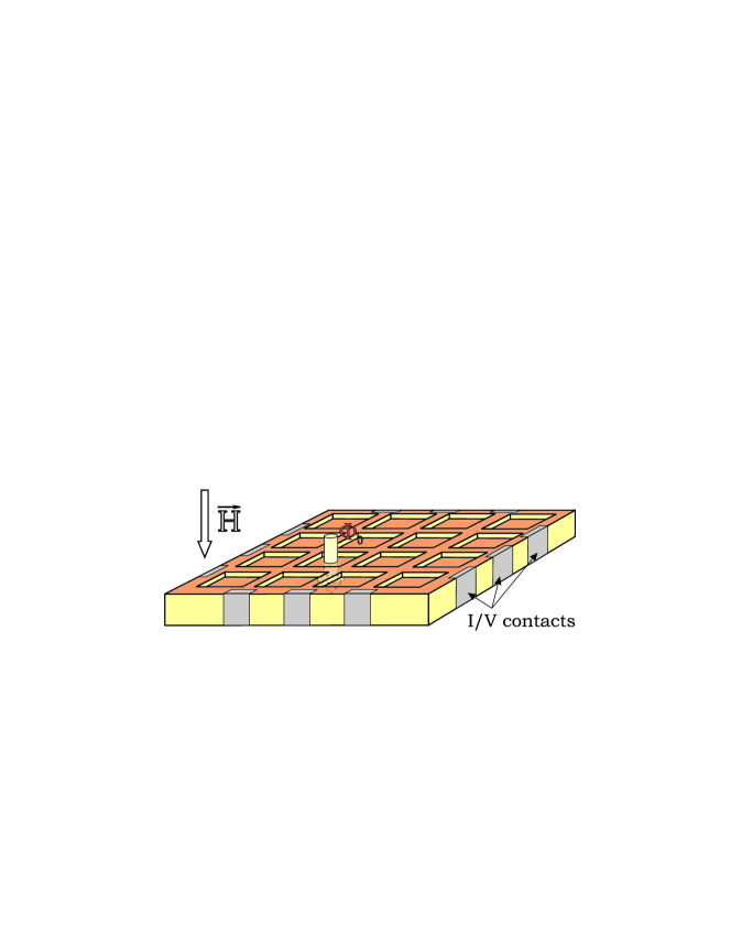
We show how a single flux quantum can be effectively manipulated in a superconducting film with a matrix of blind holes. Such a sample can serve as a basic memory element, where the position of the vortex in a matrix of pinning sites defines the desired combination of bits of information (). Vortex placement is achieved by strategically applied current and the resulting position is read-out via generated voltage between metallic contacts on the sample. Such a device can also act as a controllable source of a nanoengineered local magnetic field for e.g. spintronics applications.
Superconducting electronics has always been envisaged as a candidate for futuristic applications, thanks to its low resistance, low dissipation, and high current densities which allow for high power/size ratios. In the last decade, enormous research efforts have been delivered in the field of mesoscopic superconductivity, where samples are comparable to the characteristic superconducting length scales (coherence length and penetration depth ) and therefore exhibit pronounced quantum effects. The revealed key dynamic effects include: the step-like resistance of the superconducting elements as a function of applied current (zero resistance - ‘resistive’ state - normal state), and the corresponding definition of two critical currents resstate ; very rich ‘phase-slip’ phenomena psreview ; S- and N- shaped I-V characteristics of superconducting stripes and wires SNshape ; control of dynamic properties of the sample by perforations or magnetic structuring enhpar ; ‘ratchet’ physics, using the mobility of vortices in applied current across asymmetric pinning potentials ratchet . The latter is the current pivotal axis of the field of fluxonics, the research area exploiting duality between electrons and superconducting flux quanta in electromagnetic fields.
In this Letter we show the use of fluxonics in a superconducting matrix, i.e. the manipulation of a single vortex in a square sample with arrays of blind holes (see Fig. 1). As we will show, such a sample can act as a superconducting memory device, with individually addressable memory cells and without restrictions on read/write cycles. Additionally, the sample can act as a spatially controllable field source, which is of use in nanoscale spintronics and hybrid structures.
The concept of here presented devices is based on the following electron-vortex analogies: (i) an electric current drives vortices in the same manner as an electromagnetic field drives electrons (Lorentz force), and (ii) moving vortices produce voltages similar to mobile electrons producing electric currents. To characterize this behavior, we use the suitably modified time-dependent Ginzburg-Landau equation Kramer
| (1) |
coupled with the equation for the electrostatic potential
| (2) |
Note that the last term in Eq. (1) accounts for the variable thickness of the sample , while equations remain averaged in the -direction (i.e. uniform distribution of all quantities is assumed across the sample thickness) bhgolib . In Eqs. (1-2), the distance is measured in units of , is scaled by its value in the absence of magnetic field , time by , vector potential by , and the electrostatic potential by . is directly proportional to inelastic electron-collision time , and equals 10 in the present calculation, and parameter is taken from Ref. Kramer . The normal-metal leads where current is injected in the sample (see Fig. 1) satisfy , where is the injected current density in units of , with . Edges of the samples are modeled by the Neumann boundary condition at superconductor/vacuum interfaces. Here considered samples are thin, and we may therefore neglect the screening of the applied magnetic field , and take =(,,0) in Eq. (1). Nevertheless, this still allows us to eventually calculate the magnetic response of the sample, using to obtain the supercurrent density in the sample.
The key idea of the superconducting memory is to have the position of a single vortex represent one combination of several bits of data. For example, to possibly store all combinations of four bits of data, one needs logic states. To represent this in a superconducting memory based on just one vortex, we need a sample with 16 possible single-vortex states. We illustrate one possible candidate in Fig. 1, where the vortex can be located in any of the 4x4 blind holesblhole . Because vortices in mesoscopic superconductors generally favor central positions in the sample, due to interaction with strong Meissner currents at sample edges, it is necessary to nano-engineer such samples with sufficiently spaced, large and deep holes such that each one of them is capable to pin a vortex. In what follows, we focus on a sample with size and thickness , with uniformly distributed square blind holes of size and depth (i.e. with bottom thickness , see Fig. 1).
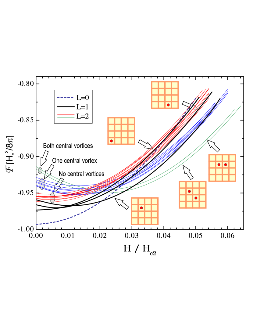
In Fig. 2, we show the behavior of the above described superconducting sample in applied perpendicular magnetic field. At a given value of the magnetic field, we search through the Gibbs energy landscape for all stable states, with or without vortices. The free energy is calculated using , where is the sample volume). In Fig. 2, we show the energy levels obtained for states with vorticity . Although there are 16 stable states (further denoted by , with a vortex located in -th hole in -, and -th hole in -direction), only three energy levels exist (two quadruple, and one octuple degenerate) due to the four-fold sample symmetry (see insets in Fig. 2). In the case of two vortices, we find 21 distinct energy levels for 120 possible states foot1 . In our memory cell, we aim to use a single vortex scenario, although state offers storage of additional 120 bit-combinations. The reason is that two vortices are much more difficult to control simultaneously in the present concept, but this possibility should not be entirely disregarded.
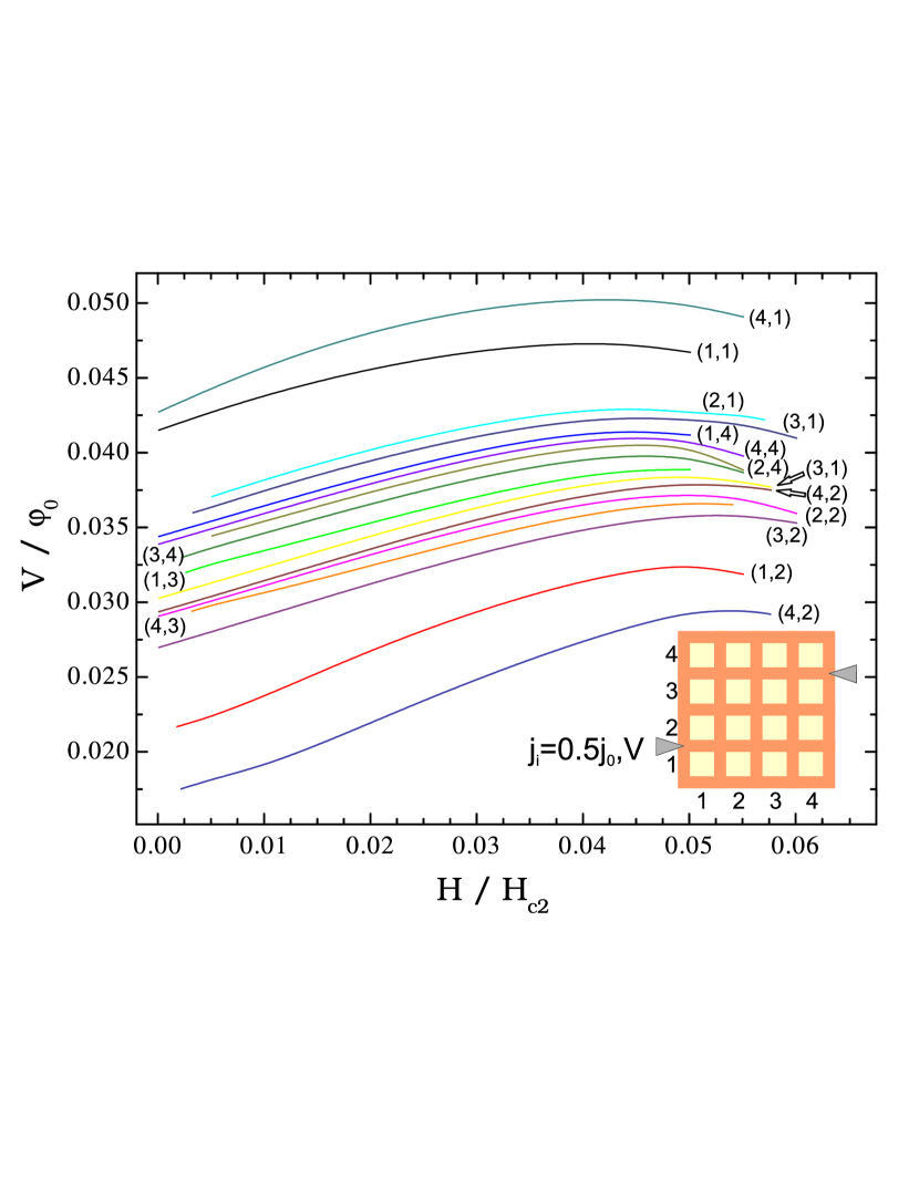
If each of the possible positions of one vortex in our memory cell is to represent a combination of bits, we must first enable successful readout of those states, and the degeneracy of energy levels in Fig. 2 is not helpful. For that reason, we suggest injection of a weak test current in the sample, and that in a diagonal direction across the cell. In that case, the vortex, regardless of its position, will experience a Loretzian force perpendicular to the applied current, but its response will depend on its exact position. For example, the energy-degenerate vortex states and will feel the drive towards the interior of the sample and out of the sample, respectively, and their energy levels must split. To detect these subtle differences, we propose the measurement of voltage between the current leads. Since we use the normal-metal leads, the normal current survives in the superconducting sample up to certain characteristic length. However, the length over which the non-equilibrium quasiparticles can exist in the sample ( being the diffusion constant Denis1 ) is typically larger than the size of a mesoscopic sample. For that reason, in our memory cell the normal current can reach the lead across the sample, and a finite voltage can be detected foot3 . The measured voltage due to injected quasiparticles will depend on their entire path and Andreev recombinations at the vortex core, and will therefore differ for every position of the vortex in the matrix. We show this in Fig. 3, as an evolution of the calculated voltage between the leads as a function of applied field, for small injected current , and all 16 possible states in their full stability range. Since indeed all 16 voltages clearly differ, this enables the successful read-out of the vortex position.
In order to write the data in the memory cell, we must realize single-vortex manipulation at nanoscale. For that we use the same principle - the Lorentzian behavior of vortices in an applied current. Sufficiently large current will be able to depin the vortex from the residing hole and push it towards another location. Of course, to move the vortex from one particular position to another, one must apply the current strategically. For example, to move the vortex from location to , the current could be applied between columns 2 and 3 to move the vortex ‘right’, and additionally between rows 3 and 4 to move the vortex down. Alternatively, the latter two currents can be combined in one, as shown in Fig. 4. Successful vortex hopping can be monitored by measured voltage at the current leads, as it leaves a distinct feature (maximum) in the voltage vs. time characteristics.
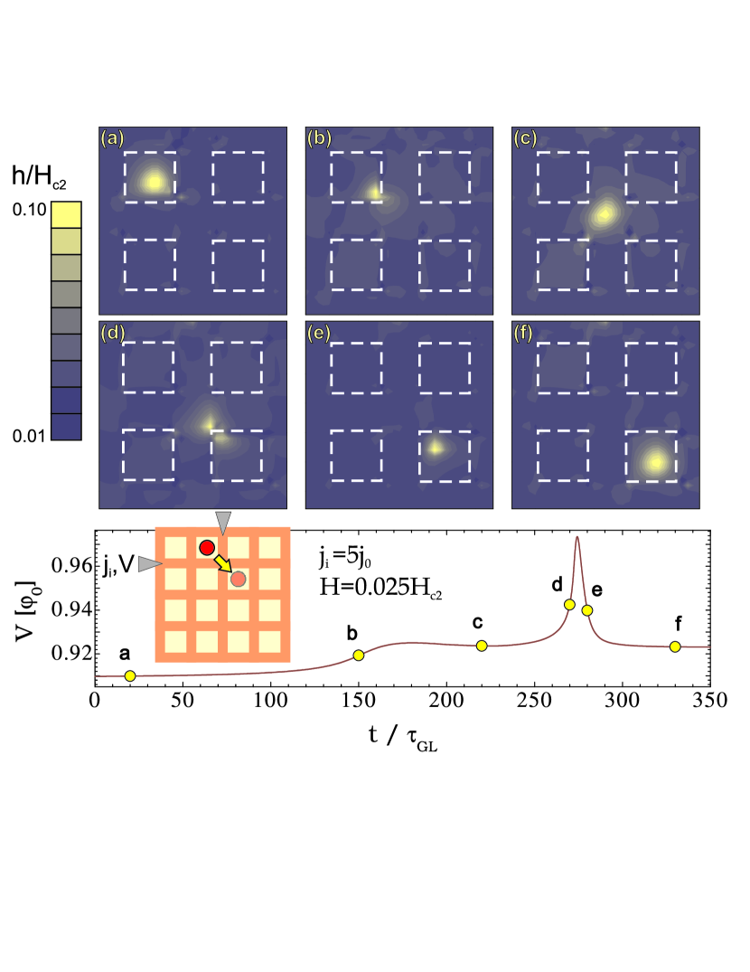
Fig. 4 also shows the magnetic field profile under the sample, resulting from a vortex in motion. Such localized and moveable sources of magnetic field recently became of significant technological relevance, thanks to the prediction of Berciu et al. janko . Namely, electronic and spin states in dillute-magnetic-semiconductors (DMS) seem to be very responsive to a non-homogeneous magnetic field, and can be trapped under a vortex core in a DMS-superconductor bilayer. This also means that those spins and charges can be manipulated by manipulating vortices, and our device provides the needed control. Besides its potential for spintronics, manipulation of the vortex position can also provide controllable switching for magnetic cellular automata imre .
Finally, we reflect on few potential problems of the device. Since the vortex in our system is driven by an applied current, the magnitude of the current is of outmost importance. Obviously, the lowest current needed for the successful readout is determined by the sensitivity of the voltage measurement, but can easily be in the nA range. However, the current needed for the vortex manipulation from one pin to the other strongly depends on the strength of the pinning site. This justifies our choice of blind holes, since they are able to hold the vortex, but not as strongly as a full perforation. Additionally, blind holes enable direct visualization of the vortex core, and testing of the device by low-temperature magnetic magn and tunneling STM scanning probe measurements. Depending on the size and depth of the hole, the threshold current for vortex depinning has to be determined foot5 . Used current in the device has to be close to the minimal needed one, since a larger current may force the vortex to overshoot the desired position, even leave the sample, and very large injected current can cause phase-slippage, finite resistance and dissipation resstate . On a positive note, these error scenarios are detectable, since each trapping of the vortex in a hole causes minima, and vortex exit maxima in the measured voltage versus time milokanda . In summary, although latter issues and its operation at low temperatures hamper the applicability of the device, we have here demonstrated the proof of concept for a single-vortex superconducting matrix with a high level of control. This concept is verifiable in experiment, it has an intuitive application as a superconducting memory, and can lead to further developments of e.g. controllable nanoscale field sources for applications in hybrid devices.
This work was supported by the Flemish Science Foundation (FWO-Vl), the Belgian Science Policy (IAP), the ESF-NES and ESF-AQDJJ networks.
References
- (1) B. I. Ivlev and N. B. Kopnin, Usp. Fiz. Nauk 142, 435 (1984) [Sov. Phys. Usp. 27, 206 (1984)].
- (2) I. M. Dmitrenko, Low. Temp. Phys. 22, 648 (1996).
- (3) D. Y. Vodolazov, F. M. Peeters, L. Piraux, S. Mátéfi-Tempfli, and S. Michotte, Phys. Rev. Lett. 91, 157001 (2003).
- (4) M. V. Milošević, G. R. Berdiyorov, and F. M. Peeters, Phys. Rev. Lett. 95, 147004 (2005).
- (5) C. S. Lee, B. Jankó, I. Derényi and A.-L. Barabási, Nature (London) 400, 337 (1999); C. C. de Souza Silva, J. Van de Vondel, M. Morelle and V. V. Moshchalkov, Nature (London) 440, 651 (2006).
- (6) L. Kramer and R. J. Watts-Tobin, Phys. Rev. Lett. 40, 1041 (1978).
- (7) G. R. Berdiyorov, M. V. Milošević, B. J. Baelus, and F. M. Peeters, Phys. Rev. B 70, 024508 (2004).
- (8) A. Bezryadin and B. Pannetier, J. Low Temp. Phys. 102, 73 (1996); A. Bezryadin, Yu. N. Ovchinnikov, and B. Pannetier, Phys. Rev. B 53, 8553 (1995); S. Raedts, A. V. Silhanek, M. J. Van Bael, and V. V. Moshchalkov, Phys. Rev. B 70, 024509 (2004); G. R. Berdiyorov, M. V. Milošević, and F. M. Peeters, New J. Phys. 11, 013025 (2009).
- (9) The size of the holes is insufficient to trap both vortices, otherwise the number of possible states would be 136, with 24 distinct energy levels.
- (10) is typically 50-100 V in low-Tc samples, and can be significantly higher in high-Tc materials. is approximately in the A/cm2 range, making the injected current in this case c.a. 0.1-1 A.
- (11) D. Yu. Vodolazov, D. S. Golubović, F. M. Peeters, and V. V. Moshchalkov, Phys. Rev. B 76, 134505 (2007).
- (12) Therefore, even in the fully superconducting state, the sample exhibits a non-zero resistance due to the metallic leads.
- (13) The Ginzburg-Landau time is typically in the 1-10 ps range at intermediate temperatures.
- (14) M. Berciu, T. G. Rappoport, and B. Janko, Nature (London) 435, 71 (2005).
- (15) A. Imre, G. Csaba, L. Ji, A. Orlov, G. H. Bernstein, and W. Porod, Science 311, 205 (2006).
- (16) A. Oral, S. J. Bending and M. Henini, Appl. Phys. Lett. 69, 1324 (1996); E. W. J. Straver, J. E. Hoffman, O. M. Auslaender, D. Rugar, and K. A. Moler, Appl. Phys. Lett. 93, 172514 (2008).
- (17) T. Cren, D. Fokin, F. Debontridder, V. Dubost, and D. Roditchev, Phys. Rev. Lett. 102, 127005 (2009); I. Guillamón, H. Suderow, A. Fernández-Pacheco, J. Sesé, R. Córdoba, J. M. De Teresa, M. R. Ibarra, and S. Vieira, Nature Phys. 5, 651 (2009).
- (18) For an Al cell with given geometrical parameters, we obtained a depinning current of A.
- (19) M. V. Milošević, A. Kanda, S. Hatsumi, F. M. Peeters, and Y. Ootuka, Phys. Rev. Lett. 103, 217003 (2009).